minimizes the transconductance and drain current temperature variations. Based on these results, a current-reused CG-LNA with good temperature performance is designed. At ambient temperatures, the CG-LNA has a measured power gain of 10.3 dB and a noise figure (NF) of 4.3 dB at 15.2 GHz, while consuming 4.5 mA from a 1.3-V power supply. When the temperature varies from 253 to 393 K, the CG-LNA has a power gain variation of 3 dB, NF variation of 2 dB, and dc power consumption variation of 11.9%. This paper is the first to report the temperature effect on -band CG-LNAs.
Index Terms—CMOS, common gate, current reuse, low-noise amplifier (LNA), zero temperature coefficient.
I. INTRODUCTION
D
EEP-SUBMICROMETER CMOS technology offers a promising solution for highly integrated transceivers in emerging microwave and millimeter-wave broadband wireless communications. An essential design consideration in the above transceivers is to maintain the required performance over a wide range of temperatures. In the literature, only a few studies address this problem on the common-source low-noise amplifier (CS-LNA) configuration [1], [2]. Kaamouchi et al. evaluated the 2.4-GHz CS-LNA in 0.13- m silicon-on-in-sulator (SOI) CMOS technology over a temperature range from 298 to 473 K [1]. If the transistor is properly biased at the zero-temperature-coefficient point of transconductance , the measured power gain variation in that study is 0.9 dB and noise figure (NF) variation is 2.3 dB over a 175-K Manuscript received December 23, 2008; revised May 01, 2009. First pub-lished August 11, 2009; current version pubpub-lished September 04, 2009.W.-L. Chen is with the Department of Electrical Engineering, National Chung Cheng University, Chiayi 62102, Taiwan, and is also with the National Nano De-vice Laboratories, Hsinchu 300, Taiwan (e-mail: [email protected]; wenlin. [email protected]).
S.-F. Chang is with the Department of Electrical Engineering, the Depart-ment of Communications Engineering, and the Center for Telecommunication Research, National Chung Cheng University, Chiayi 62102, Taiwan (e-mail: [email protected]).
K.-M. Chen is with National Nano Device Laboratories, Hsinchu 300, Taiwan (e-mail: [email protected]).
G.-W. Huang is with National Nano Device Laboratories, Hsinchu 300, Taiwan, and also with the Department of Electronics Engineering, National Chiao Tung University, Hsinchu 300, Taiwan (e-mail: [email protected]).
J.-C. Chang is with the United Microelectronics Corporation, Hsinchu 300, Taiwan.
Digital Object Identifier 10.1109/TMTT.2009.2027074
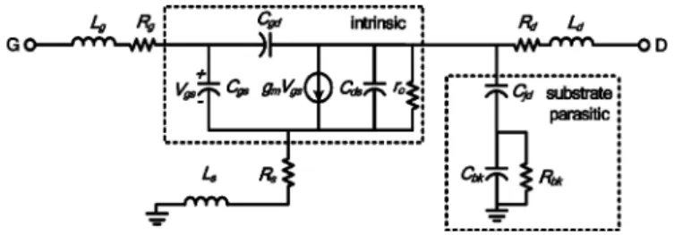
Fig. 1. Small-signal model of NMOSFET.
temperature range. Another study reports an SiGe BiCMOS CS-LNA at 5.5 GHz having a power gain variation of 0.4 dB and an NF variation of 0.5 dB from 273 to 373 K by incor-porating a proportional-to-absolute temperature compensation circuit [2].
Recent research highlights the advantages of the common-gate low-noise amplifier (CG-LNA) for microwave and mil-limeter-wave applications because of its susceptibility to process tolerance [3], [4]. However, the performance variation of this CG-LNA due to the temperature effect has not been explored. This paper, therefore, designs an NMOS LNA with the stacked common-gate topology. Section II investigates the temperature variations of the NMOS transistor and spiral inductor. Section III then designs a CG-LNA to evaluate the temperature effect on circuit performance. Section IV describes the measured results. Finally, Section V provides a conclusion.
II. TEMPERATUREEFFECT ONNMOSFETANDSPIRAL INDUCTORDEVICECHARACTERISTICS
A. NMOS Transistor
The threshold voltage and carrier mobility strongly vary with temperature in NMOS transistors. This, in turn, results in the pronounced temperature dependence of the transconductance and noise parameter. To examine the temperature-dependence effect, this paper uses an NMOS transistor with a total gatewidth of 57.6 m and gate-length of 0.12 m for testing. A small-signal model including the substrate parasitic [5] is selected for device characterization, as Fig. 1 shows. In this model, the in-trinsic elements include , , , and . , , ,
, and represent the extrinsic elements and , and represent the substrate parasitic.
1) Zero-Temperature-Coefficient Biases: Fig. 2(a) illustrates
the measured drain current versus over the temperature range from 253 to 393 K. When is less than 0.3 V, the drain current varies strongly with temperature. The drain current 0018-9480/$26.00 © 2009 IEEE
2132 IEEE TRANSACTIONS ON MICROWAVE THEORY AND TECHNIQUES, VOL. 57, NO. 9, SEPTEMBER 2009
Fig. 2. Measured: (a)I –V and (b) g –V relationship in the temperature range from 253 to 393 K.
becomes almost unchanged with temperature when equals 0.62 V. This bias condition is the zero temperature coefficient point of the drain current . When the NMOS transistor is biased at , the drain current exhibits negligible tem-perature variation.
By differentiating with respect to , the temperature de-pendence of the extrinsic transconductance is obtained, as indi-cated in Fig. 2(b). This shows that variation with temperature nearly disappears at V. This particular bias point is called the zero-temperature-coefficient point of
transconduc-tance .
To compromise between the temperature variation of drain current and transconductance, the bias condition of an NMOS transistor is generally chosen between and . This paper selects a gate bias of V, which leads to
mS and mA over 253–393 K.
2) Element Extraction: The authors of [5]–[7] used element
extraction methods to extract the small-signal elements based on the measured scattering parameters. First, the on-wafer mea-surement of the NMOS transistor biased at V and
Fig. 3. MeasuredS-parameters of the NMOS transistor from 0.5 to 20 GHz.
V was performed at various temperatures from 253 to 393 K to obtain the scattering parameters from 0.5 to 20 GHz, as shown in Fig. 3. Based on these results, the extraction pro-cedure was performed to obtain the extrinsic and substrate par-asitic elements and then the intrinsic elements. This procedure was repeatedly performed at each temperature of 253, 313, 353, and 393 K.
The extrinsic and substrate parasitic elements are
, pH, , pH,
, pH, fF, fF,
and k at ambient temperature. Fig. 4 shows that intrinsic capacitors also vary slightly with temperature, which
are fF, fF, and fF. Compared to
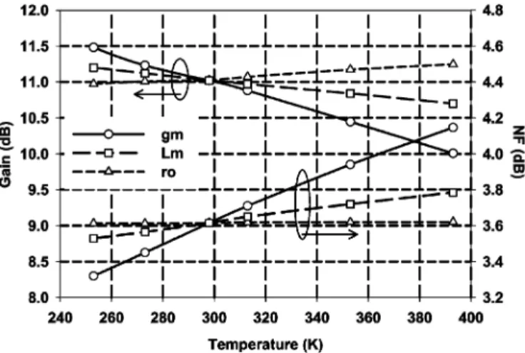
the above weakly temperature-varying elements, the intrinsic and have relatively greater temperature variation, where the intrinsic varies from 29.2 to 25.3 mS ( 13.7% variation) and increases from 316 to 336 ( 6.3% variation) from 253 to 393 K.
B. Spiral Inductor
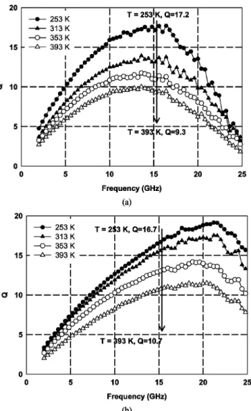
In addition to the NMOS transistor device, the passive spiral inductor is also affected by temperature [1]. Fig. 5 shows the variation of the quality factor with temperature for 2.5- and 1.68-nH spiral inductors in 0.13- m CMOS technology. These inductors are laid out on an M8 layer with 3.5/2.5 turns of the metal line, having a 2- m thickness, 6- m linewidth, and 2- m line spacing. The measurement results in Fig. 5 indicate that the quality factor decreases when temperature increases. At 15 GHz, the quality factor of the 2.5-nH inductor decreases from 17.2 to 9.3 and the 1.68-nH inductor decreases from 16.7 to 10.7 over 253–393 K. These experiment results shows that there is no apparent inductance change over the temperature range. This implies that the quality factor is primarily degraded by increasing parasitical resistance.
III. DESIGN OFCURRENT-REUSEDCG-LNA
Fig. 6(a) shows that a CG-LNA is composed of two common-gate NMOS transistors, which are stacked together for sharing
Fig. 4. Temperature dependence of the intrinsic elements: transconductance, output resistance, and parasitic capacitances (V gs = 0:5 and V ds = 0:6 V).
the same dc current to reduce the dc power consumption. As in Section II, the intrinsic capacitances and are small enough that the small-signal model of the CG-LNA can be sim-plified to Fig. 6(b).
Fig. 5. Measured quality factor of the spiral inductor. (a) 2.5 nH. (b) 1.68 nH.
A. Circuit Design
As in Section II, the gate bias voltage is set at V for minimal temperature variation of the transconductance and the drain current. As pointed out in [3], the coupling effect between the channel and gate becomes important at high frequencies, and may deteriorate the gain and noise performance. This effect is included in the gate conductance [3] as follows:
(1) where is the channel conductance at zero drain-to-source voltage. Define as the ratio of to the transconductance
, i.e., , and it approximates to
(2) In the equation above, is the ratio of the transconductance to the channel conductance at zero drain-to-source
voltage, and is the unity current
2134 IEEE TRANSACTIONS ON MICROWAVE THEORY AND TECHNIQUES, VOL. 57, NO. 9, SEPTEMBER 2009
Fig. 6. Proposed current-reused stacked CG-LNA. (a) Schematic. (b) Small-signal equivalent circuit.
Fig. 7. Effects of the transconductance, output resistance, and matching induc-tors on gain and NF of the CG-LNA at 15.2 GHz.
GHz. Hence, at 15 GHz, implying a negligible channel-gate coupling effect in this case.
By taking into account the gate–source capacitance , the input impedance of becomes
(3)
Fig. 8. Simulated results of the designed CG-LNA over 253–393 K. (a) Power gain. (b) Return losses. (c) NF.
where denotes the impedance at the drain node. If , can be simplified as
Fig. 9. Microphotograph of the proposed current-reused CG-LNA.
The inductor is added at the source node to resonate so that . The input impedance of at can then be expressed as
(5) To match to , must satisfy the following equation:
(6) Section II shows that is nearly temperature independent and and have the opposite temperature coefficients. Therefore, the determination of inter-stage matching inductance based on (6) is valid for a wide temperature range. In other words, a good return loss can be maintained over 253–393 K.
If input is matched, the effective transconductance becomes (7) Equation (7) indicates that the temperature variation of LNA gain is dominated by the temperature dependence of . The temperature variation of power gain can be minimized if the bias is carefully designed at the zero-temperature-coefficient point, as discussed in Section II-A.
Regarding noise performance, the noise factor is given by
(8)
Fig. 10. Measured results of the designed CG-LNA over 253–393 K. (a) Power gain. (b) Return losses. (c) NF.
where is the channel thermal noise coefficient and
from [7]. The bias-dependent coefficients , , and are nearly unchanged with temperature because the bias has been properly selected close to the zero-temperature-coefficient point. This also minimizes the temperature effect on the NF.
2136 IEEE TRANSACTIONS ON MICROWAVE THEORY AND TECHNIQUES, VOL. 57, NO. 9, SEPTEMBER 2009
TABLE I
COMPARISON OFCMOS LNAs
B. Simulation
By using the measured temperature coefficients of the NMOS transistor and spiral inductors in Section II, the temperature de-pendence of the CG-LNA is simulated. First, the contribution from the respective temperature coefficient of the transconduc-tance , the output resistance , and the spiral inductor is simulated. Fig. 7 shows that the power gain decreases by 1.5 dB and the NF increases by 0.9 dB at 15.2 GHz when decreases from 29.2 to 25.3 mS. When increases from 316 to 336 , the power gain changes slightly by 0.25 dB and the NF remains nearly unchanged. The spiral inductors induce 0.5-dB gain reduction and 0.3-dB NF increments. These simulation re-sults show that the temperature coefficient of dominates the power gain and NF temperature performance of the CG-LNA.
Next, the total effect from the temperature property of , , and on the CG-LNA performance is simulated. Fig. 8 shows the simulated frequency response 253, 313, and 393 K, respectively. The power gain reduction from 253 to 393 K is around 2.1 dB at 15.2 GHz. This gain reduction is about the same at other frequencies in the 13–18-GHz range. Over the temperature range of 253–393 K, the input return loss is better than 17 dB and the output return loss is better than 10 dB from 14.2 to 16.2 GHz. The NF has an increment of 1.9 dB from 253 to 393 K at 15.2 GHz, and this increment is about the same at other frequencies in 6–18 GHz.
C. CMOS Layout
The proposed current-reused CG-LNA was implemented in 0.13- m CMOS technology. The inductors (1.1 nH), (0.9 nH), (1.7 nH), and (1.4 nH) were realized with a spiral structure, and the RF-bypassing gate capacitance was implemented with a 2.5-pF metal–insulator–metal capac-itor. All gate bias resistors of 10 k were realized using n poly resistors. Fig. 9 shows a chip photograph, which covers an area of 0.6 mm including the input and output pads.
IV. MEASUREMENTRESULTS OFCURRENT-REUSEDCG-LNA The implemented NMOS LNA was on-wafer measured with HP8510 vector network analyzer and NP5 noise measurement systems. Fig. 10 depicts the measured frequency performance at various temperatures (253, 313, and 393 K). At 313 K, the power gain is 10.3 dB and the input and output return losses are better than 15.6 dB at 15.2 GHz, respectively.
The input is 14.8 dBm and the input IP3 is 5 dBm. The NF is 4.3 0.2 dB over a broad frequency range of 6–18 GHz, presenting a wideband noise characteristic. The implemented CG-LNA consumes 4.5 mA from a 1.3-V power supply. When the temperature increases from 253 to 393 K, the power gain at 15.2 GHz monotonically decreases by 3 dB and the NF increases from 3.9 to 5.9 dB over the 140-K variation range. The similar power gain reduction of 3 dB and the NF increment of 2 dB are also seen at other frequencies in the 13–18 GHz. The drain current increases from 4.2 to 5 mA, corresponding to a 11.9% variation over the 140-K variation range. The input and output return losses are better than 10 dB in 14–16 GHz, which implies that the input and output match is less affected by temperature. The measurement results agree very well with the simulation ones in Fig. 8, except the mod-erate degradation in the output return loss.
Table I outlines the measured performance of the proposed CG-LNA and other CS-LNAs. In terms of temperature per-formance, only a few CS-LNA studies in [1] and [2] have conducted temperature performance measurements, and this paper is the first to report the temperature performance of the -band CG-LNA topology. Among these chips in Table I, the 5.5-GHz SiGe CS-LNA [2] achieves the smallest power gain temperature variation (0.4 dB/100 K) and moderate NF variation (0.5 dB/100 K) over the 273–373-K range. This out-standing temperature variation performance is attributed to the incorporation of a proportional-to-absolute temperature com-pensation circuit. However, the dc power consumption variation (34%/100 K) is relatively large. For the 2.4-GHz CS-LNA in SOI technology [1], it also has a large dc power consumption variation of 68%/175 K, while it has excellent gain temperature
inductor are experimentally obtained in a range from 253 to 393 K. First, the zero temperature coefficient points of the drain current and transconductance are obtained such that the dc-bias condition of the NMOS transistor can be determined. This, in turn, makes it possible to minimize the drain current and transconductance variation with temperature. This paper also extracts the temperature variation of intrinsic and extrinsic elements of the NMOS small-signal model from the measured scattering parameters. Based on these results, this paper designs a current-reused CG-LNA in 0.13- m CMOS technology. At room temperature, the implemented CG-LNA has a measured power gain of 10.3 dB and NF of 4.3 dB at 15.2 GHz, while consuming 4.5 mA from a 1.3-V power supply. When the tem-perature changes from 253 to 393 K, the CG-LNA has a power gain variation of 3 dB, NF variation of 2 dB, and a dc power consumption variation of 11.9%. This paper demonstrates that the temperature performance of the NMOS CG-LNA in the -band can be optimized simply by selecting the proper transistor bias, which provides a simple, but effective method of minimizing the temperature effect.
ACKNOWLEDGMENT
The authors would like to thank Dr. S.-Y. Huang, United Mi-croelectronics Corporation, Hsinchu, Taiwan, and S.-C. Wang and H.-H. Hu, both with the Department of Electronics Engi-neering, National Chiao Tung University, Hsinchu, Taiwan, for their technique support.
REFERENCES
[1] M. E. Kaamouchi, M. S. Moussa, J.-P. Raskin, and D. Vanhoenacker-Janvier, “Zero-temperature-coefficient biasing point of 2.4-GHz LNA in PD SOI CMOS technology,” in Proc. 2nd Eur. Microw. Integ. Cir-cuits Conf., Oct. 2007, pp. 303–306.
[2] H. A. Ainspan, C. S. Webster, J. O. Plouchart, and M. Soyuer, “A 5.5-GHz low noise amplifier in SiGe BiCMOS,” in Proc. 24th Solid-State Circuits Conf., Sep. 1998, pp. 80–83.
[3] X. Guan and A. Hajimiri, “A 24-GHz CMOS front-end,” IEEE J. Solid-State Circuits, vol. 39, no. 2, pp. 368–373, Feb. 2004.
[4] B. Razavi, “A 60-GHz CMOS receiver front-end,” IEEE J. Solid-State Circuits, vol. 41, no. 1, pp. 17–22, Jan. 2006.
[5] S. Y. Huang, K. M. Chen, G. W. Huang, D. Y. Yang, and C. Y. Chang, “Characterization and modeling of RF MOSFETs under hot carrier stress and oxide breakdown,” in Silicon Monolithic Integr. Circuits in RF Syst. Top. Meeting, Long Beach, CA, Jan. 18–20, 2006, pp. 81–84.
Wen-Lin Chen (S’04) was born in Changhua,
Taiwan, in 1977. He received the B.S. and M.S. degrees in electrical engineering from Chung Yuan Christian University, Jhongli City, Taiwan, in 2000 and 2002, respectively, and is currently working toward the Ph.D. degree at National Chung Cheng University, Chiayi, Taiwan.
In 2005, he joined National Nano Device Labora-tories (NDL), Hsinchu, Taiwan, where he is currently an Assistant Researcher. His research interests in-clude microwave and millimeter-wave integrated circuit (IC) design and RF characterization of semiconductor devices.
Sheng-Fuh Chang (S’83–M’92–SM’07) received
the B.S. and M.S. degrees in communications engineering from National Chiao Tung University, Hsinchu, Taiwan, in 1982 and 1984, respectively, and the Ph.D. degree in electrical engineering from the University of Wisconsin–Madison, in 1991.
He was involved with high-power microwave and millimeter-wave sources, including free-electron lasers and Cerenkov masers, with the Center for Plasma Theory and Computation, University of Wisconsin–Madison. In 1992, he joined the Hyton Technology Corporation, where he was responsible for C- and Ku-band satellite low-noise down-converter and multipoint microwave distribution system (MMDS) transceivers. In 1994, he joined the Department of Electrical Engineering, National Chung Cheng University, Chiayi, Taiwan, where he is currently a Professor with the Department of Electrical Engineering and Department of Communications Engineering, and is also the Director of the Center for Telecommunication Research. His research interests include micropower electromagnetic vital signal detection, wireless indoor locating techniques, monolithic phased arrays, and microwave/millimeter-wave mono-lithic integrated circuits.
Prof. Chang is a member of Phi Tau Phi and Sigma Xi.
Kun-Ming Chen received the M.S. and Ph.D.
de-grees in electronics engineering from National Chiao Tung University, Hsinchu, Taiwan, in 1996 and 2000, respectively.
In 2000, he joined the National Nano Device Laboratories, Hsinchu, Taiwan, as an Associate Researcher, and became a Researcher in 2007. His research interests include microwave device processes and characterization.
2138 IEEE TRANSACTIONS ON MICROWAVE THEORY AND TECHNIQUES, VOL. 57, NO. 9, SEPTEMBER 2009
Guo-Wei Huang (S’94–M’97) was born in Taipei,
Taiwan, in 1969. He received the B.S. and Ph.D. de-grees in electronics engineering from National Chiao Tung University, Hsinchu, Taiwan, in 1991 and 1997, respectively.
In 1997, he joined National Nano Device Labora-tories (NDL), Hsinchu, Taiwan, where he is currently a Researcher and Manager of the High-Frequency Technology Division. Since August 2008, he has been an Adjunct Associate Professor with the Department of Electronics Engineering, National
Chiao Tung University. His current research interests focus on characterization and modeling techniques of high-frequency devices and characterization and verification of RF integrated circuits (RFICs)/monolithic microwave integrated circuits (MMICs).
Jen-Chung Chang, photograph and biography not available at time of