DESIGN OF LOW-LEAKAGE POWER-RAIL ESD CLAMP
CIRCUITS IN NANOSCALE CMOS TECHNOLOGY
:
:
DESIGN OF LOW-LEAKAGE POWER-RAIL ESD CLAMP
CIRCUITS IN NANOSCALE CMOS TECHNOLOGY
Student: Federico Agustín Altolaguirre
Advisor: Prof. Mind-Dou Ker
A Thesis
Submitted to EECS Graduate Program National Chiao Tung University in partial Fulfillment of the Requirements
for the Degree of Master
July 2011
:
(Gate Tunneling)
(Power-Rail ESD Clamp Circuit)
(Silicon-Controlled Rectifier, SCR) 65 65 ( 21.6 µA) 112 nA (Human-Body-Model, HBM) (Machine-Model, MM)
DESIGN OF LOW-LEAKAGE POWER-RAIL
ESD CLAMP CIRCUITS IN NANOSCALE
CMOS TECHNOLOGY
Student: Federico A. Altolaguirre Advisor: Prof. Ming-Dou Ker
EECS International Graduate Program of
Electrical and Computer Engineering College
National Chiao Tung University
ABSTRACT
The aim of this thesis is to design an ultra-low leakage power-rail ESD clamp in an advanced CMOS technology. The principle is using circuit techniques to reduce the leakage current of the circuit, without undermining the ESD robustness. This thesis is divided in three main parts
The first part introduces the evolution of gate-tunneling research. With the gate-oxide thickness become thinner and thinner in CMOS processes, the phenomena become more and more serious. In the past research, the mechanisms and formulas of gate-tunneling have been observed. The model of gate-tunneling also has been applied into advance CMOS processes.
In the second part, the proposed solution is presented and the simulation results are shown, using the SPICE models for a 65-nm CMOS process with thin-oxide devices. In the traditional power-rail ESD clamp, the leakage through the MOS capacitor is extremely high. The proposed solution includes a novel design technique to reduce this leakage, and a series of implementations are presented and detailed.
In the third part, a test chip is realized and sent to tape-out to realize further analysis. The standby leakage of the circuits is measured, and the ESD robustness is measured by several parameters, such as TLP, turn-on verification, and HMB/MM simulation. The proposed circuits can lead to a leakage current as low as 112nA under 1V-bias at 25°C (opposed to 21.6µA of the traditional power-rail ESD clamp), while the ESD robustness is not changed.
- iii -
Acknowledgements
I would like to thank to Professor Ming Dou Ker for all his support and guidance to make this work possible. Also I thank to National Chiao Tung University and the Electronics Engineering and Computer Science International Graduate Program to allow me to study in such a good university (EECS IGP).
I would like to thank to Po Yen Chiu for his infinite patience, dedication, and help. My special thanks also to MA-TEK for their professional support with the ESD testing and failure analysis.
My appreciation to all my labmates and professors, especially to Professor Zheng, who has not yet lost her hopes for me to learn Chinese.
I would like to show my appreciation to Professor Pedro Julián and the Laboratory of Micro/Nano Electronics (LMNE) UNS-CIC, Argentina, for without their support I would not be here.
Special thanks to my parents, Mónica and Alberto, to my brother, Francisco, and to my friends, the ones I left in Argentina and to the ones I made in here, to Luciano, Juan, Javier, Marcelo, Nerio, Christian, Agustín, Edgar, Quito, Rodrigo, Xinyi, Facundo, Luz, Leo (Argentina), Leo (Taiwan), and all the others I am forgetting their names. Thanks to all of them for their support and love.
Lastly, I would like to thanks especially to Elisa, for giving to me all her strengths, and to her family, who has already adopted me as another member.
I am very happy to finally have reached this point, and I am very sure this is all thanks to all of you, so once more, thank you very much, and I hope someday I can return all the favors and support you have given to me.
Sincerely,
iv
Table of Contents
Abstract (Chinese) ... i Abstract (English) ... ii Acknowledgements ... iv Table of Contents ... vTable Captions ... vii
Figure Captions ... viii
Chapter 1. Introduction ... 1
1.1 Motivation ... 1
1.2 Thesis Organization ... 2
Chapter 2. Gate Leakage in Nanoscale CMOS Processes ... 4
2.1 Background ... 4
2.2 Gate Tunneling Mechanisms Described with Energy-Band Diagram ... 6
2.3 Gate Direct Tunneling Current Model in BSIM4 ... 10
2.3.1 Gate-to-Substrate Current (Igb=Igbacc+Igbinv) ... 11
2.3.2 Gate-to-Channel Current (Igc0) and Gate-to-S/D (Igs and Igd) ... 12
2.3.3 Partition of Igc ... 13
2.3 Gate Direct Tunneling Current Model in BSIM4 ... 14
Chapter 3. Ultra-Low Leakage Power Rail ESD Clamp Circuits ... 17
3.1 Traditional Power-Rail ESD Clamp with Gate Leakage Consideration ... 17
3.2 Previous Works ... 24
3.3 Proposed Designs ... 27
3.3.1 Proposed Design A ... 28
3.3.2 Proposed Design B ... 31
3.3.3 Proposed Design C ... 34
3.3.4 Comparison between Circuit Simulations ... 36
Chapter 4. Experimental Results ... 38
4.1 Device Characteristics ... 40
v
4.3 TLP Measurements ... 43
4.4 Turn-On Verification ... 46
4.5 HBM and MM ... 48
Chapter 5. Discussions ... 55
5.1 SCR Driving Strength vs. Performance ... 55
5.2 Proposed Design C Failure Analysis ... 55
5.3 Sources of Leakage in the Proposed Designs ... 59
5.2 More discussions on Measurement Results ... 59
Chapter 6. Conclusions and Future Work ... 60
6.1 Conclusions ... 60
6.2 Future Work ... 60
TABLE CAPTIONS
Chapter 3
Table 3.1. Leakage current of NMOS and PMOS capacitor in different CMOS processes
... 18
Table 3.2. Traditional power-rail ESD clamp circuit ... 20
Table 3.3. Traditional power-rail ESD clamp circuit with level restorer ... 24
Table 3.4. Proposed Design A ... 29
Table 3.5. Proposed Design B ... 32
Table 3.6. Proposed Design C ... 35
Table 3.7. Simulation results ... 37
Chapter 4
Table 4.1. MOS capacitor current under 1Vbia ... 41Table 4.2. Measured leakage current for the designed circuits ... 43
FIGURE CAPTIONS
Chapter 2
Fig. 2.1. Different tunneling mechanisms in Si/SiO2/Si structure. ... 7 Fig. 2.2. The tunneling mechanisms of NMOS in inversion (a) NMOS cross-sectional view in inversion (b) energy barrier figure ... 8 Fig. 2.3. The tunneling mechanisms of PMOS in inversion: (a) PMOS cross-sectional view in inversion (b) Energy barrier figure. ... 9 Fig 2.4. Schematic gate current components ... 10 Fig. 2.5. Calculated dependence of tunneling current on substrate electric field for SiO2 and HfO2 by classical and quantum mechanical (QM) models. The quantization in inversion layer lifts the electron energy up, leading to larger tunneling current ... 15 Fig. 2.6. Calculated tunneling currents vs gate voltage from classical and QM models. The QM effects are compensated in some extent due to the larger band bending in QM model. However, the enhancement due to quantization can still be observed in I-V plot for HfO2 ... 15 Fig. 2.7. Simulated electron tunneling current of N-MOSFET vs EOT for various gate dielectrics. The substrate doping is 1018cm-3 and flat band voltage is thus -1.0V. For HfSiO4, K=13 and m=0.34m0 from an average of SiO2 and HfO2 values are assumed. Al2O3 mole fraction is 30% for HfAlO and Si3N4 mole fraction 40% for optimized SiON
... 16 Fig. 2.8. Gate leakage as a function of Tinv for HfO2 for both Poly-Si and TiN gate dielectrodes. Also shown is SiON line for reference... 16
Chapter 3
Fig. 3.1. Traditional power-rail ESD clamp circuit ... 18
Figure 3.2. Power-on transient simulation for the circuit of Fig. 3.1 ... 19
Fig 3.3. ESD-like transient simulation for the circuit of Fig 3.1 ... 19
Fig. 3.4. Simulated PMOS gate current for different voltages and temperatures... 21
Fig. 3.5. Simulated NMOS gate current for different voltages and temperatures ... 21
Fig. 3.6. Modified power-rail ESD clamp circuit with level restorer ... 22
Fig. 3.7. Power-on transient simulation for the circuit of Fig. 3.6 ... 23
Fig. 3.8. ESD-like transient simulation for the circuit of Fig 3.6 ... 23
Fig. 3.9. Proposed power-rail ESD clamp circuit in reference [18] ... 25
Fig. 3.10. Proposed power-rail ESD clamp circuit in reference [19] ... 26
Fig. 3.11. Proposed power-rail ESD clamp circuit in reference [20] ... 26
Fig. 3.12. Proposed power-rail ESD clamp circuit in reference [21] ... 27
Fig. 3.13. Capacitor gating technique to overcome the gate leakage ... 27
Fig. 3.14. Proposed design A schematic ... 29
Fig. 3.15. Power-on transient simulation for the circuit of Fig. 3.14 ... 30
Fig. 3.16. ESD-like transient simulation for the circuit of Fig 3.14 ... 30
Fig. 3.17. Proposed design B schematic ... 32
Fig. 3.18. Power-on transient simulation for the circuit of Fig. 3.17 ... 33
Fig. 3.19. ESD-like transient simulation for the circuit of Fig 3.17 ... 33
Fig. 3.20. Proposed design C schematic ... 34
Fig. 3.21. Power-on transient simulation for the circuit of Fig. 3.20 ... 35
Chapter 4
Fig. 4.1 65-nm CMOS process test chip: (a) Layout top view of the test chip (b) Die photo
of the test chip ... 38
Fig. 4.2. Substrate-triggered SCR: (a) Layout top view and (b) Cross-sectional view of the substrate-triggered SCR ... 39
Fig. 4.3. Test MOS capacitors for measuring the gate leakage. (a) NMOS capacitor, (b) PMOS capacitor. Both capacitors are 20µm by 20µm ... 40
Fig. 4.4. SCR TLP IV curve ... 41
Fig. 4.5. Setup for measuring the capacitor leakage. (a) NMOS capacitor; (b) PMOS capacitor ... 42
Fig. 4.6. TLP measurements for the traditional power-rail ESD clamp circuits ... 44
Fig. 4.7. TLP measurements for the proposed design A ... 44
Fig. 4.8. TLP measurements for the proposed Design B ... 45
Fig. 4.9. TLP measurements for the proposed design C ... 45
Fig. 4.10. Comparison of VT1 against the PMOS driver width ... 46
Fig. 4.11. Comparison of the turn-on efficiency of the traditional power-rail ESD clamp circuits with parameterized PMOS SCR driver ... 47
Fig. 4.12. Comparison of the turn-on efficiency of the proposed design A with parameterized PMOS SCR driver... 47
Fig. 4.13. Comparison of the turn-on efficiency among the different power-rail ESD clamp circuits with PMOS SCR driver of size W/L=50µ m/0.15µm ... 48
Fig 4.14. Failure spot on PMOS driver in the traditional power-rail ESD clamp circuit after MM stress of 200V ... 50
Fig 4.15. Failure spot on SCR in design A after MM stress f 2f0V ... 50
Fig. 4.16. Failure on PMOS driver in design B after MM stress of 150V ... 51
Fig. 4.17. Failure on SCR in the traditional power-rail ESD clamp circuit after HBM stress of 3.5kV ... 51
Fig. 4.19. Failure on SCR in design B after HBM stress of 3.5kV ... 52 Fig. 4.20. I-V curve for the proposed design C after ESD zap. The green line is before zap and the red line after zap... 53 Fig. 4.21. Failure in proposed design C after MM stress of 50V ... 53 Fig. 4.22. Failure in proposed design C after HBM stress of 500V ... 54
Chapter 5
Fig. 5.1. Layout view of the proposed design C. The SCR is highlighted in red ... 56 Fig. 5.2. OBIRCH Image. The hotspots appear highlighted in red color ... 57 Fig. 5.2. (a) Proposed design C; (b) and (c) modifications to the proposed design C . 57
Chapter 1
Introduction
1.1 Motivation
In order to achieve less power consumption, higher operating speed, and higher integration capability, CMOS device dimensions are scaled down to smaller channel length and thinner gate-oxide thickness. Although the circuit performances can be enhanced with the evolution of CMOS processes, such small dimensions introduce some defects to the nanoscale CMOS devices. These defects have caused impacts on the integrated circuits (ICs) implemented with nanoscale CMOS processes.
Gate-tunneling current is a serious problem in nanoscale MOS transistors. As the gate oxide of MOS transistors becomes thinner and thinner, the probability that carriers escape the energy barrier increases. When the gate-oxide thickness is scaled down to several nanometers or below, the gate-tunneling current can no longer be ignored. With such a large gate-tunneling current, the CMOS ICs may not work correctly because the node voltage could be discharged through the leaky gate terminal. Therefore, the gate leakage issue must be seriously considered during the design phase of all ICs fabricated in nanoscale CMOS processes.
There are several previous works addressing the influences of gate-tunneling current on nanoscale CMOS ICs. In microprocessors, the capacity of the embedded memory is rapidly increased to improve the overall performance. In the future, memory will occupy most area in a microprocessor. However, the leakage current of the embedded static random access memory (SRAM) dominates the standby current. Reducing the leakage current of the embedded SRAM is the most important design target to achieve low power consumption [1]. In analog circuits, the gate leakage will degrade the performance if long transistors are used. Besides, mismatch among gate leakage currents in different transistors introduces other limitations [2]. The gate leakage current limits the expected performance enhancement with the evolution of CMOS processes.
Electrostatic discharge (ESD) is the most important reliability issue in ICs, and it needs to be taken into consideration during the design phase. Since ESD is not scaled down
with the CMOS technology, efficient ESD protection design for the nanoscale CMOS devices with thinner gate oxide becomes more challenging. In the whole-chip ESD protection scheme, the power-rail ESD clamp circuit plays an important role because it determines the overall ESD robustness of the IC [3]. The power-rail ESD clamp circuits are designed to provide the ESD current path between VDD and VSS during ESD stresses and to be kept off under normal power-on conditions. Traditional power-rail ESD clamp circuits were realized with RC-based ESD-detection circuit and an ESD clamping device. With the consideration on the area efficiency, the capacitor in the ESD-detection circuit was often realized with the MOS capacitor, because MOS capacitors have the largest capacitance per unit area in generic CMOS processes. However, the gate leakage current in the MOS capacitor becomes serious in nanoscale CMOS processes, because the MOS capacitor in the power-rail ESD clamp circuit is often realized with large dimensions. With the intolerable gate leakage through the MOS capacitor, the power-rail ESD protection circuit with the traditional structure cannot be used anymore. A new design to further reduce the leakage current in the power-rail ESD clamp circuit is necessary.
1.2 Thesis Organization
Chapter 2 introduces the gate-tunneling mechanisms and describes the gate-tunneling model in BSIM4 SPICE model. There are three main mechanisms which cause the gate-tunneling tunneling. All of the mechanisms are addressed and formulated. The gate-tunneling model is also applied to nanoscale CMOS transistors.
Chapter 3 discusses the gate leakage issue in the traditional power-rail ESD clamp circuits. The traditional power-rail ESD clamp circuit is simulated in a 65-nm CMOS process to investigate the impacts caused by the gate leakage current in the MOS capacitor. To reduce the leakage current in the power-rail ESD clamp circuit, a novel technique is studied and a series of power-rail ESD clamp circuits are proposed and simulated in a 65-nm CMOS process.
Chapter 4 presents the experimental results. Measured results have shown that the leakage current under normal circuit operating conditions can be significantly reduced in the proposed ultra-low leakage power-rail ESD clamp circuits as compared with the traditional designs. Moreover, the ESD robustness is not deteriorated.
Chapter 5 includes some relevant discussions and Chapter 6 presents the conclusions and future work.
Chapter 2
Gate Leakage in Nanoscale CMOS Processes
2.1 Background
The research of field-emission was the predecessor before the research of gate-tunneling. In 1897, R. W. Wood was the first person to describe the phenomenon of field-emission. He observed the phenomenon and the emission current in the discharge tube experiment. In 1926, R. A. Millikan and C. C. Lauritsen observed that the emission current was exponentially dependent on the electric field strength.
In 1928, R. Fowler and L. W. Nordheim proposed the accurate description of field emission, which is based on the tunneling of electrons through the surface potential barrier. They also derived the formula of the emission current [4], which is called the “Fowler-Nordheim Tunneling (FNT) theory.” This theory is very important and it influences the scientists who study the tunneling mechanisms of the semiconductor nowadays.
During 1940 to 1960, the development of semiconductor science started to increase, and new devices were invented one after another. But there was a small current (about 10-14A~10-11A) which observed in the metal-insulator-metal or metal-insulator- semiconductor connection [5][6]. This phenomenon and the tunneling current were the same as the “Fowler -Nordheim Tunneling”. Finally the tunneling current density [7] was given by 1 3 2 2 4(2m) 3 2 3hqE q E J exp 8 h − φ = ⋅ π φ (2.1) where h is the Plank’s constant, q is the electron charge, E is the electric field, φ is the barrier height, and m is the free-electron mass. Equation (2.1) is called the “Fowler-Nordheim equation” nowadays.
During 1960 to 1990, the CMOS technology was matured and widely spread. With the high integration capability, CMOS technology became very important in
microelectronic applications. Since the structure consisted of metal, oxide, and semiconductor, the leakage mechanism inevitably existed. The leakage phenomenon had been investigated in the MOS structure early, and then three kinds of tunneling mechanisms [8]-[10] were observed to explain the leakage in the CMOS. These mechanism are: ECB (electron tunneling from conduction band), EVB (electron tunneling from the valence band), and HVB (hole tunneling from valence band). Since the gate oxide was quite thick in the early CMOS processes, the gate leakage did not cause serious issue. During 1990 to 2000, due to the demand of high driving current, high operating speed, and lower power consumption, the CMOS technology was scaled down toward shorter channel length, thinner gate-oxide thickness, and lower power-supply voltage. As a result, the gate leakage current can no longer be ignored, because it is larger than the order of nanoamperes). To account for this effect, the gate-direct-tunneling-current model had been proposed in BSIM4 model [11]-[13] and it was released on Mar. 24, 2000 [14]. The proposed model was given by
3 3 OX 2 2 OX b 3 b n g OX OX b b OX OX V 8 2m 1 (1 ) q J C(V , V , T , ) exp 8 h 3hq E − π φ − − φ = ⋅ φ ⋅ π φ ε (2.2) and g OX b OX g OX OX b b bo b OX V V V 20 C(V , V , T , ) exp ( 1) (1 ) ( ) N T α − φ φ = + ⋅ − ⋅ ⋅ φ φ φ (2.3)
where VOX is the effective gate voltage, TOX is the oxide thickness, EOX is VOX/TOX, α is the fitting parameter depending on the tunneling process, φbo is the Si/SiO2 barrier height (3.1eV for electron and 4.5eV for hole), and φb is the actual tunneling barrier height (3.1eV for ECB, 4.2eV for EVB, and 4.5eV for HVB). N represents the density of carriers in the inversion or accumulation layer of the injecting electrode. For ECB and EVB tunneling process in both the inversion and accumulation regimes, N is expressed by
ge th g FB OX inv t acc t OX inv t acc t V V V V N n v ln 1 exp( ) n v ln 1 exp T n v n v − − ε = ⋅ + + ⋅ + − (2.4)
where ninv and nacc denote the swing parameters, Vth is the threshold voltage, VFB is the flat-band voltage, vt is the thermal voltage, and Vge is the gate voltage minus the gate-depletion voltage (Vg-Vpoly).
For EVB tunneling process, N can be described as
OX g OX EVB t OX EVB t V N n v ln 1 exp T n v − φ ε = ⋅ ⋅ + (2.5)
where φg is Eg/q and nEVB is the fitting parameter.
2.2 Gate Tunneling Mechanisms Described With Energy-Band
Diagram
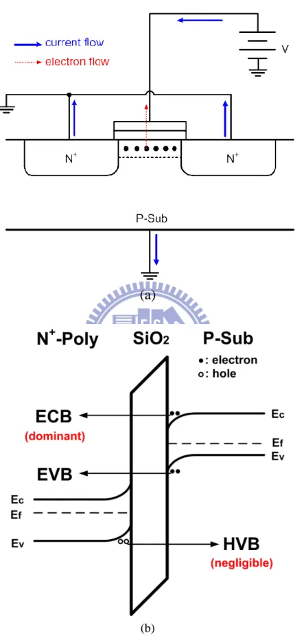
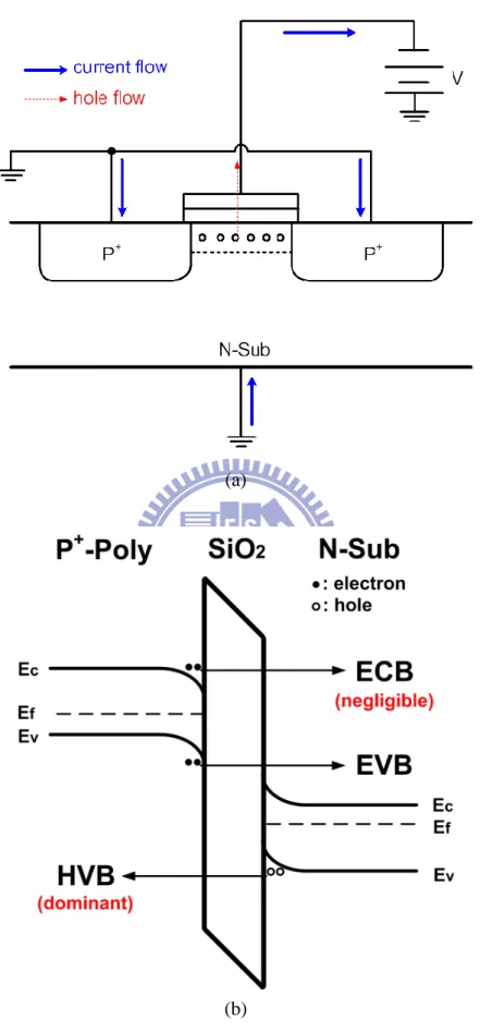
Three kinds of tunneling mechanisms were observed to explain the leakage in CMOS technology, which are shown in Fig. 2.1. ECB is the electron tunneling from the conduction band across the oxide barrier. ECB basically needs 3.1eV before the electron has the probability to tunnel across the oxide barrier. EVB is the electron tunneling from the valence band across the oxide barrier. EVB basically needs 4.2eV before the electron has the probability to tunnel across the oxide barrier. HVB is the hole tunneling form the valence band across the oxide barrier. HVB basically needs 4.5eV before the hole has the probability to tunnel across the oxide barrier.
The main tunneling mechanism of NMOS is shown in Fig. 2.2. The N+-Poly gate is connected to the high potential to create the inversion layer, so the electron energy band is reduced in the N+-Poly side. Respectively, the electron energy band is raised in the P-Sub side. Since the inversion layer is full of electron and is connected to an N+ region, it has higher electron energy than that of the P-Sub region. Consequently, the electron has higher probability to tunnel. Therefore, ECB is the main tunneling mechanism of NMOS in inversion. On the other hand, the N+-Poly energy band has larger hole energy. The HVB can be ignored because the hole is the minority carrier in the N+-Poly region.
The main tunneling mechanism in PMOS is shown in Fig. 2.3. The P+-Poly gate is connected to the low potential to create the inversion layer, so the P+-Poly electron energy
band is raised. Respectively, the P-Sub electron energy band is reduced. Since the inversion layer is full of holes and is connected to a P+ region, it has higher hole energy than that of the N-Sub region. Consequently, the hole has higher probability to tunnel. Therefore, HVB is the main tunneling mechanism of PMOS in inversion. On the other hand, the P+-Poly energy band has larger electron energy. The ECB can be ignored because the electron is minority carrier in the P+-Poly region.
(a)
(b)
Fig. 2.2. The tunneling mechanisms of NMOS in inversion (a) NMOS cross-sectional view in inversion (b) energy barrier figure.
(a)
(b)
Fig. 2.3. The tunneling mechanisms of PMOS in inversion: (a) PMOS cross-sectional view in inversion (b) Energy barrier figure.
2.3 Gate Direct Tunneling Current in BSIM4
As the gate oxide thickness is scaled down to several nanometers or below, the gate leakage current becomes large due to direct tunneling of the carriers. The tunneling current happens between the gate terminal and silicon beneath the gate oxide. To reduce the tunneling current, different kinds of gate dielectrics have been studied to replace the traditional SiO2. To maintain good interface with the substrate, multi-layer dielectric stacks have being proposed. The BSIM4 gate tunneling model has been demonstrated to work for multi-layer gate stacks as well. The gate direct tunneling components are shown in Fig. 2.4. The components include the tunneling current between the gate and substrate (Igb) and the current tunneling current between the gate and channel (Igc), which is partitioned between the source and drain terminals by Igc = Igcs + Igcd. The third component exists between the gate and source/drain diffusion regions (Igs and Igd).
2.3.1 Gate-to-Substrate Current (Igb=Igbacc+Igbinv)
Igbacc, which is determined by ECB (electron tunneling from conduction band), is significant in accumulation and is given by
(
)
gbacc eff eff oxRatio gb aux
oxacc oxacc
I W L A T V V
exp B TOXE(AIGBACC BIGBACC V ) 1 CIGBACC V
= ⋅ ⋅ ⋅ ⋅ ⋅ − ⋅ − ⋅ ⋅ + ⋅ . (2.6) ToxRatio in (2.6) is expressed by NTOX oxRatio 2 TOXREF 1 T TOXE TOXE = ⋅ . (2.7) Vaux in (2.6) is given by gb fbzb aux t t V V
V NIGBACC v log[1 exp( )]
NIGBACC v
−
= ⋅ ⋅ +
⋅ . (2.8)
Igbinv, which is determined by EVB (electron tunneling from valence band), is significant in inversion and is given by
(
)
gbinv eff eff oxRatio gb aux
oxdepinv oxdepinv
I W L A T V V
exp B TOXE(AIGBINV BIGBINV V ) 1 CIGBINV V
= ⋅ ⋅ ⋅ ⋅ ⋅ − ⋅ − ⋅ ⋅ + ⋅ . (2.9) ToxRatio in (2.9) is expressed by NTOX oxRatio 2 TOXREF 1 T TOXE TOXE = ⋅ . (2.10) Vaux in (2.9) is given by oxdepinv aux t t V EIGBINV
V NIGBINV v log 1 exp( )
NIGBINV v − = ⋅ ⋅ + ⋅ . (2.11)
2.3.2 Gate-to-Channel Current (I
gc0) and Gate-to-Source/Drain (I
gsand
Igd)
Igc0, which is determined by ECB (electron tunneling from conduction band) for NMOS and HVB (hole tunneling from valence band) for PMOS at Vds=0, is formulated as
(
)
gc0 eff eff oxRatio gse aux
oxdepinv oxdepinv
I W L A T V V
exp B TOXE(AIGC BIGC V ) 1 CIGC V
= ⋅ ⋅ ⋅ ⋅ ⋅ − ⋅ − ⋅ ⋅ + ⋅ . (2.12) ToxRatio in (2.12) is expressed by NTOX oxRatio 2 TOXREF 1 T TOXE TOXE = ⋅ . (2.13) Vaux in (2.12) is given by gse aux t t V VTH
V NIGC v log 1 exp( )
NIGC v − = ⋅ ⋅ + ⋅ . (2.14)
Igs represents the gate tunneling current between the gate and the source diffusion region, while Igd represents the gate tunneling current between the gate - drain diffusion region. Igs and Igd are determined by ECB for NMOS and HVB for PMOS, respectively. Igs is expressed as
gs eff oxRatioEdge gs gs '
gs ' gs '
I W DLCIG A T V V
exp B TOXE POXEDGE (AIGS BIGS V )(1 CIGS V )
= ⋅ ⋅ ⋅ ⋅ ⋅ − ⋅ ⋅ ⋅ − ⋅ + ⋅ . (2.15) ToxRationEdge is given by NTOX oxRatioEdge 2 TOXREF 1 T ( )
TOXE POXEDGE (TOXE POXEDGE)
= ⋅
⋅ ⋅ . (2.16)
(
)
2 4 gs ' gs fbsd V = V −V +1.0e− . (2.17) Vfbsd’ is given by B fbsd k T NGATE V log( ) VFBSDOEF q NSD = + . (2.18) Igd is expressed as gd eff oxRatioEdge gd gd ' gd ' gd ' I W DLCIGD A T V Vexp B TOXE POXEDGE (AIGD BIGD V )(1 CIGD V )
= ⋅ ⋅ ⋅ ⋅ ⋅ − ⋅ ⋅ ⋅ − ⋅ + ⋅ . (2.19) Vgs’ is given by
(
)
2 4 gd ' gd fbsd V = V −V +1.0e− . (2.20)2.3.3 Partition of I
gcConsidering the drain bias effect, Igc is split into two components, Igcs and Igcd, namely, Igc=Igcs+Igcd. Igcs is given by
4 dseff
gcs gc0 2 2 4
dseff
PIGCD V exp( PIGCD) 1 1.0e
I I PIGCD V 2.0e − − ⋅ + − − + = ⋅ ⋅ + . (2.21) PIGCD is expressed as dseff 2 gsteff gsteff V B TOXE PIGCD (1 ) V 2 V ⋅ = − ⋅ . (2.22) Igcd is given by
4 dseff
gcd gc0 2 2 4
dseff
1 (PIGCD V 1) exp( PIGCD) 1.0e
I I PIGCD V 2.0e − − − ⋅ + ⋅ − + = ⋅ ⋅ + (2.23)
2.4 Gate Leakage Improvement with High-K Gate Dielectric
The drain current of MOS transistors is given by
2 ox GS th DS DS 1 W I C 2(V V )V V 2 L = µ − − . (2.24)
In order to have high driving current, the oxide thickness is reduced to achieve larger Cox. The larger Cox not only increases the driving current but also increases the operating speed. However, the interface will exist direct tunneling when the oxide thickness is scaled down to several nanometers or below. The situation becomes worse as the oxide thickness becomes thinner. In order to avoid the large gate leakage current, different kinds of gate dielectrics have been studied to replace the traditional SiO2. In other words, using other dielectrics can increase the oxide thickness without decreasing the driving current. The capacitance in the dielectric layer is
0 d k C T ε = . (2.25)
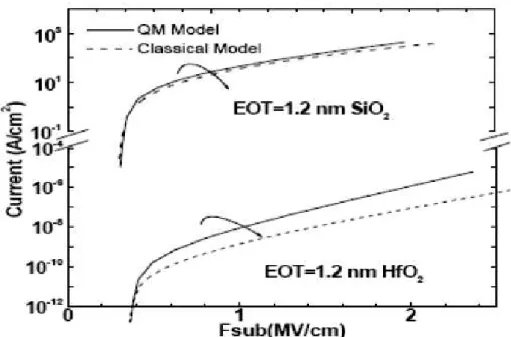
Using high-k dielectrics can increase the capacitance and maintain high driving current even if the thickness is thicker than that of SiO2. To maintain good interface with substrate, multi-layer stacked dielectric layers had been proposed. Experiment results indicate that the leakage current was significantly be improved by using high-K dielectric [15] [16] and the gate leakage improvement form different kinds of gate dielectrics are shown in Fig. 2.5-Fig. 2.8.
Fig. 2.5. Calculated dependence of tunneling current on substrate electric field for SiO2 and HfO2 by classical and quantum mechanical (QM) models. The quantization in inversion layer lifts the electron energy up, leading to larger tunneling current [15].
Fig. 2.6. Calculated tunneling currents vs gate voltage from classical and QM models. The QM effects are compensated in some extent due to the larger band bending in QM model. However, the enhancement due to quantization can still be observed in I-V plot for HfO2 [15].
Fig. 2.7. Simulated electron tunneling current of N-MOSFET vs EOT for various gate dielectrics. The substrate doping is 1018cm-3 and flat band voltage is thus -1.0V. For HfSiO4, K=13 and m=0.34m0 from an average of SiO2 and HfO2 values are assumed. Al2O3 mole fraction is 30% for HfAlO and Si3N4 mole fraction 40% for optimized SiON [16].
Fig. 2.8. Gate leakage as a function of Tinv for HfO2 for both Poly-Si and TiN gate dielectrodes. Also shown is SiON line for reference [16].
Chapter 3
Ultra-Low Leakage Power-Rail ESD Clamp Circuits
3.1 Traditional Power-Rail ESD Clamp with Gate Leakage Consideration
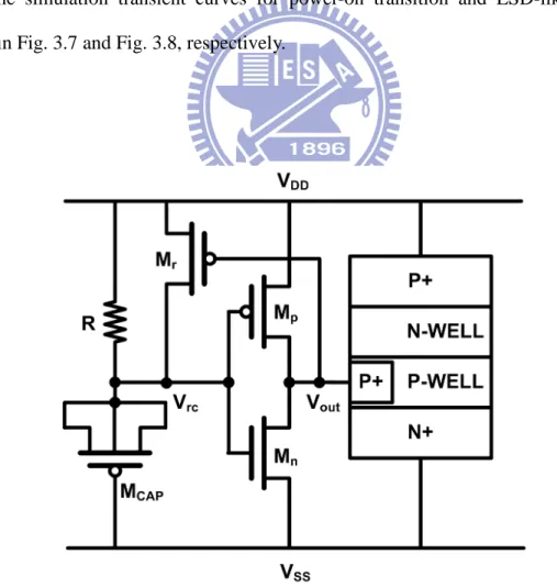
The traditional power-rail ESD clamp circuit is composed of an ESD clamp device, such as a MOSFET or Silicon Controlled Rectifier (SCR), and a trigger circuit. This trigger circuit is in charge of detecting the ESD stresses and activating in time the protection device to sink the ESD current through a safe path. The trigger circuit often includes an RC delay stage to detect the fast-transient nature of the ESD stress, and a set of transistors to trigger the main protection device. A schematic of this circuit is shown in Fig. 3.1.
The circuit of Fig. 3.1 is designed and simulated using the SPICE models for a 65-nm CMOS technology. The circuit is comprised by an RC delay circuit formed by the resistor R and the PMOS capacitor MCAP, a trigger circuit formed by the transistors Mp and Mn, and an SCR as protection clamp. The transistor Mp is large-sized to provide the SCR trigger current. Notice that an SCR has been used instead of a MOSFET; this is done basically because the SCR is known to have the best ESD robustness-per-area [17], and as the operating voltages in this technology fall below the SCR holding voltage, there is no latch-up issue.
Under a positive ESD pulse zapping the node VDD (VSS grounded), the initial value of Vrc is kept to ~0V. The capacitor MCAP then charges up the node Vrc with the time constant RC (in the order of microseconds). As the node Vrc remains low, the transistor Mp is turned on and drives the trigger current to the SCR, causing the SCR to turn on to protect the internal circuits.
Table 3.1
Leakage current of NMOS and PMOS capacitor in different CMOS processes.
Generation MOS Type tox
Total Gate Current at 1V (W/L = 1 µm / 1 µm) 90-nm NMOS ~2.3nm ~11nA PMOS ~2.5nm ~3nA 65-nm NMOS ~2.0nm ~140nA PMOS ~2.2nm ~80nA 45-nm NMOS ~1.9nm ~260nA PMOS ~2.1nm ~95nA
0 100 200 300 400 500 0.0 0.2 0.4 0.6 0.8 1.0 Time (µµµµs) V o lt a g e ( V ) VDD VRC
Leakage Current from VDD
16 18 20 22 24 26 28 30 C u rr e n t ( µ A )
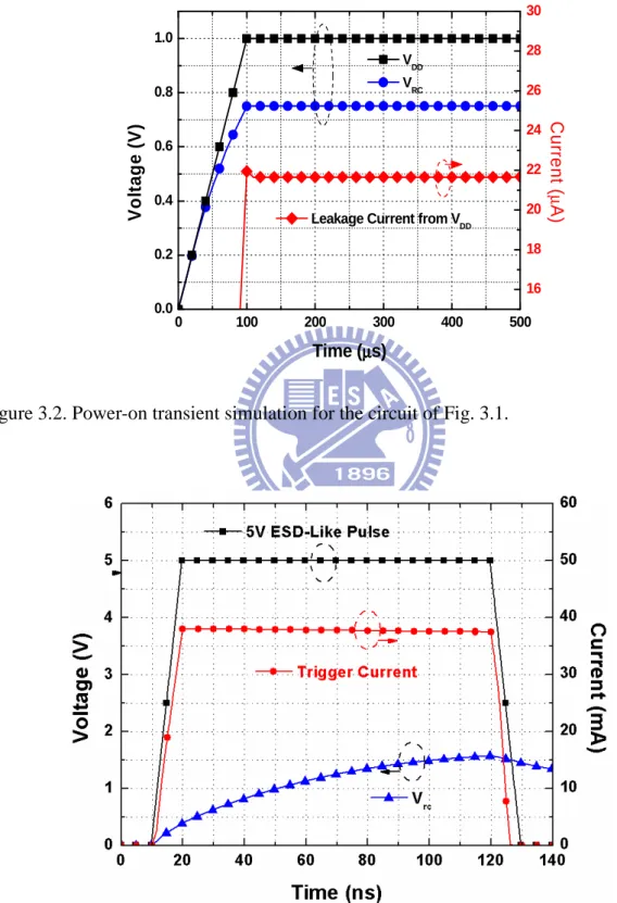
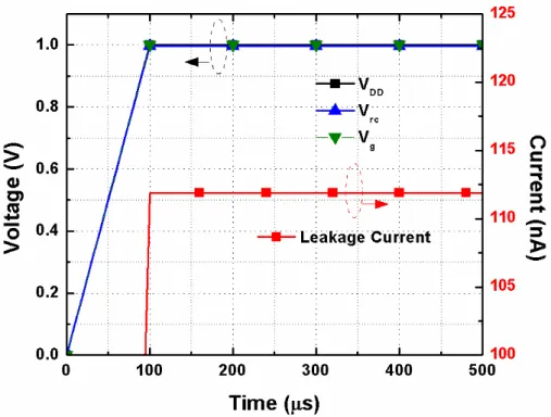
Figure 3.2. Power-on transient simulation for the circuit of Fig. 3.1.
Table 3.2
Traditional power-rail ESD clamp circuit.
Transistor size (µm/µm)
R (kΩ)
Mn Mp MCAP
1/0.15 50/0.15 20/20 50
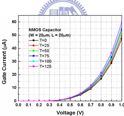
Under normal circuit operation the capacitor MCAP presents high impedance, so the voltage at the node VRC is kept to VDD. Therefore, Mp and Mn are turned off and on, respectively, so the SCR trigger point is tied to VSS, maintaining the SCR in off state. The RC time constant of the capacitor MCAP and resistor R is fast enough (in the order of µs) so the RC delay stage can follow the VDD transient voltage and there are no misstriggers during the power-on ramp (usually 100µs to 1ms). In advanced CMOS technologies, there is a leakage current through the capacitor (MCAP), which induces a voltage drop across the resistance R. Therefore, the voltage at the node Vrc is lower than VDD. This voltage difference prevents the transistor Mp to be fully turned off. There is another source of leakage across the transistors Mp and Mn, which increases the total leakage current. A table with the comparison of this leakage across different technologies is given in Table 3.1, also, Fig. 3.4 and Fig. 3.5 shows the MOS capacitors current for different voltages and temperatures. According to simulations, the total leakage current of the traditional power-rail ESD clamp circuit under 1 Volt bias is 21.6µA. In addition, if the protection device used is an NMOS transistor, as the node Vout is not fully biased to VSS the transistor is not fully turned off so there is a leakage current flowing through the transistor, increasing even more the circuit leakage current.
Fig. 3.4. Simulated PMOS gate current for different voltages and temperatures.
Fig. 3.5. Simulated NMOS gate current for different voltages and temperatures.
The simulation transient curves for power-on transition and ESD-like event are shown in Fig. 3.2 and Fig. 3.3, respectively.
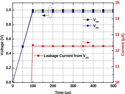
A modification of the power-rail ESD clamp circuit is shown in Fig. 3.6. It consists on adding a level restorer (Mr) in the node Vrc. This transistor biases the node Vrc to VDD. Therefore, the transistor Mp is fully turned off and there is no leakage current through Mp, and also the node Vout is fully tied to VSS so there is no leakage through the protection device. Being the node Vrc at the VDD voltage, the voltage drop in MCAP provokes a current to flow. Therefore, even though the leakage is reduced, the leakage due to the gate tunneling is still high (13µA in the simulations under 1V bias).
Even though the leakage current can be halved by the level restorer, it is still high. Therefore, changes need to be introduced in order to decrease the total leakage current to the order of nanoamperes.
The simulation transient curves for power-on transition and ESD-like event are shown in Fig. 3.7 and Fig. 3.8, respectively.
0 100 200 300 400 500 0.0 0.2 0.4 0.6 0.8 1.0 V o lt a g e ( V ) Time (µµµµs) 10 11 12 13 14 15
Leakage Current from VDD
VDD VRC C u rr e n t ( µµµµ A )
Fig. 3.7. Power-on transient simulation for the circuit of Fig. 3.6.
Table 3.3
Traditional power-rail ESD clamp circuit with level restorer.
Transistor size (µm/µm)
R (kΩ)
Mn Mp Mr MCAP
1/0.15 50/0.15 1/0.15 20/20 50
3.2 Previous Works
Some previous works have addressed the leakage issue and different designs have been proposed to overcome the leakage current in the power-rail ESD clamp circuit [18] - [21]. These circuits use different circuit techniques to either reduce the capacitance value, or the voltage applied to the capacitor under normal operation; either the capacitance or voltage reduction helps reducing the leakage through the capacitor.
The work shown in Fig. 3.9 [18] uses a series of stacked diode-connected transistors to reduce the MOS capacitor voltage under normal operation. The diode-connected PMOS transistors are used to bias the node of VB to reduce the voltage across the MOS capacitor. The static current through diode-connected PMOS transistors can be reduced by increasing their channel lengths. With enough diode-connected PMOS transistor stacked between VDD and VSS, the voltage across the MOS capacitor can be decreased to reduce the leakage current. PMOS capacitor is used in the new proposed ESD-detection circuit because the MOS capacitor is not connected to VSS and it has less gate leakage current than NMOS capacitor. The work shown in Fig. 3.10 [19] uses a different technique to achieve a similar result. The transistor Mp1 is used to generate the SCR trigger circuit under an ESD stress. The transistor Mn1 is turned on under normal operation to tie the SCR trigger node to VSS therefore guarantying the SCR is kept in off state during normal
microseconds to distinguish ESD events from normal power on transitions. The diode-connected transistors Mp2 and Mp3 act as start-up circuit with initial gate-to-bulk current from VDD to the ESD detection circuit, and in time to conduct some current
through the transistor Mc1 to bias the internal nodes.
Another power-rail ESD clamp circuit using different paths to extend the delay time and reduce RC value to solve the fast power-on issue is shown in Fig. 3.11 [20].
Recent work has reported that the MOS capacitor can be replaced by a MOM capacitor, without a significant increase in area [21].
Even though all these techniques success at reducing the leakage, it is done at expense of area overhead or the leakage remains large.
Fig. 3.10. Proposed power-rail ESD clamp circuit in reference [19].
Fig. 3.12. Proposed power-rail ESD clamp circuit in reference [21].
3.3 Proposed Designs
Fig. 3.13. Capacitor gating technique to overcome the gate leakage.
The novel circuit technique presented in Fig. 3.13 is the main focus of this thesis. The basic idea behind this technique is to actively control the MOS capacitor gate plate to
selectively drive the node to either VDD or VSS. When the node is connected to VSS, the RC delay stage is connected and the circuit behaves as the traditional power-rail ESD clamp circuit described in Fig. 3.1; when the node is tied to VDD there is no voltage drop through the capacitor, as the other node is biased to VDD by the resistor. Therefore, the capacitor leakage is nulled.
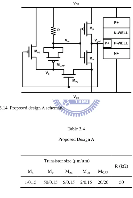
3.3.1 Proposed Design A
The circuit presented in Fig. 3.14 is the first and most straightforward implementation of the circuit technique described above. The switches are implemented with the transistors Mpg and Mng, and the trigger circuit is implemented by the transistors Mn and Mp. The RC time constant is designed to be 0.1µs.
On power-on, the node VDD raises to its full voltage with a slow time-rise (100µs to 1ms). As the rise time is slower than the RC time constant, the node Vrc can follow VDD. Therefore, the transistor Mp is turned off, as its gate-source voltage remains ~0V. Moreover, the transistor Mn is turned on, tying the node Vout to VSS, maintaining the SCR in turn-off state. As the node Vout is ~0V, the transistor Mng is turned off and the transistor Mpg is turned on, driving the node Vg to VDD. Therefore, both capacitor nodes, Vrc and Vg are biased to VDD, so the capacitor gate leakage current is nulled.
When a positive ESD pulse is zapping at VDD (VSS grounded) the fast rise time nature of the discharge keeps the node Vrc low, so the transistor Mp is turned on and drives the node Vout high. As the node Vout is higher than VSS, the transistor Mng is turned on, tying the node Vg to VSS, so the capacitor terminal is connected to ground and therefore the node Vrc start charging with the RC time constant. The node Vrc remains lower than the inverter (Mp and Mn) turning point during the ESD zap (set as a design consideration). Therefore, the node V remains high and drives the trigger current to the SCR, assuring
the SCR turns on and therefore protecting the internal circuits from damage.
The simulation transient curves for power-on transition and ESD-like event are shown in Fig. 3.15 and Fig. 3.16, respectively.
Fig. 3.14. Proposed design A schematic.
Table 3.4 Proposed Design A Transistor size (µm/µm) R (kΩ) Mn Mp Mng Mpg MCAP 1/0.15 50/0.15 5/0.15 2/0.15 20/20 50
Fig. 3.15.Power-on transient simulation for the circuit of Fig. 3.14.
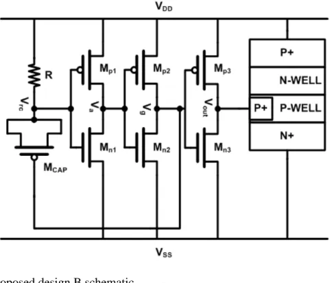
3.3.2 Proposed Design B
The circuit presented before can be modified as shown in Fig. 3.17. Two more transistors are added to the original design, and the SCR trigger point is connected to the third inverter instead of the first. The capacitor bottom node remains tied to Vg.
On power-on, the node Vrc follows VDD, so Mp1 is turned off and Mn1 is turned on. Therefore, the node Va is tied to VSS, so the transistors Mp2 and Mn2 are turned on and off, respectively, tying the node Vg to the VDD voltage. As Vg is driven to VDD, the node Vout is tied to VSS by the transistor Mn3, thus assuring the SCR remains in off state during normal operation. Also, as the nodes Vrc and Vg are both driven to VDD, there is no leakage path through the transistor. Therefore, the gate leakage current is canceled.
The behavior under ESD is similar to the previous circuit. When a positive ESD zaps at the node VDD (VSS grounded) the node Vrc remains initially low, so the transistor Mp1 is turned on and the transistor Mn1 is turned off. Therefore, the node Va is driven to the VDD voltage. Moreover, the transistors Mn2 and Mp3 (Mp2 and Mn3) are turned on (turned off), and the node Vg (Vout) is tied to VSS (VDD). As the node Vg is kept at VSS, the capacitor MCAP starts charging the node Vrc with the RC time constant, thus assuring this node to remain low during the duration of the ESD-like event. Therefore, the transistor Mp3 remains turned on during all the duration of the ESD-like event, thus driving the SCR trigger current and assuring the protection of the internal circuits.
The simulation transient curves for power-on transition and ESD-like event are shown in Fig. 3.8 and Fig. 3.19, respectively.
Fig. 3.17. Proposed design B schematic. Table 3.5 Proposed Design B Transistor size (µm/µm) R (kΩ) Mn1 Mp1 Mn2 Mp2 Mn3 Mp3 MCAP 1/0.15 5/0.15 2/0.15 10/0.15 5/0.15 50/0.15 20/20 50
Fig. 3.18. Power-on transient simulation for the circuit of Fig. 3.17.
3.3.3 Proposed Design C
The circuits mentioned above use RC circuit delay, but this topology can be inverted, i.e., the capacitor is connected between VDD and Vrc, and the resistor between Vrc and VSS. With this change, the output voltage of the delay stage is an exponential decay under input steps (such as ESD events), on the opposite to the RC delay stage, whereas the output voltage increases exponentially. Two inverter stages are needed to trigger the SCR. The resulting circuit is plotted in Fig. 3.12.
Fig. 3.20. Proposed design C schematic.
The main operation of this circuit is similar to the previous ones. Under normal circuit operation, the node Vrc remains at ~0V, so Vout is biased at VSS, tying both capacitor nodes at VSS, thus suppressing the capacitor leakage. Under a positive ESD pulse zapping at VDD (VSS grounded), the node Vrc is originally biased at VDD, and starts decaying exponentially with the RC time constant. As long as Vrc remains higher than the first inverter turning point, M remains turned on, driving the SCR triggering current.
Table 3.6 Proposed Design C Transistor size (µm/µm) R (kΩ) Mn1 Mp1 Mn2 Mp2 MCAP 1/0.15 25/0.15 1/0.15 50/0.15 20/20 50
Fig. 3.22. ESD-like transient simulation for the circuit of Fig 3.20.
3.3.4. Comparison between Circuit Simulations
All the circuits were simulated to test the behavior under power-on input ramps and ESD-like events (high transient pulses). Table 3.7 shows a comparison for the simulated total leakage current of the trigger circuits under 1V bias. It can be seen that the total leakage current of the power-rail ESD clamp circuits can be reduce down to two levels of magnitude with the proposed designs.
Table 3.7 Simulation results
Circuit
Leakage current under 1V bias Traditional power-rail ESD clamp circuit 21.6µA
Modified power-rail ESD clamp circuit 12µA
Power-rail ESD clamp circuit with gating technique 112nA Power-rail ESD clamp circuit with gating technique and
inverter chain
Chapter 4
Experiment Results
The circuits proposed in Section 3 were design in a 65-nm CMOS process and send to tape-out. The test chip, shown in Fig. 4.1, contains all the proposed circuits with parameterized SCR driving strength to test the effect of the SCR driving strength on the ESD performance. The PMOS driver was design for each circuit to be 50µm/0.15µm, 80µm/0.15µm, and 100µm/0.15µm. The sizes of the other transistors were adjusted if necessary from the values shown in Tables 3.2 to 3.7 to pass the simulations (see discussion at Section 5.1). All the circuits use an identical SCR, designed in the area of 40µm by 7.8µm. The purpose of this is to test the effect of the different trigger circuits in the ESD performance. Also, a standalone SCR and MOS capacitors were included on the test chip for testing purpose.
The experimental measurements are divided in 5 sections. The first section includes the devices characteristics, such as the SCR performance and capacitor leakage. The second section comprises the designed power-rail ESD protection circuits’ leakage current at operating voltage. The last three sections include the ESD characterization and performance, such as TLP measurements, turn-on verification, and HBM and MM simulation.
(b)
Fig. 4.1 65-nm CMOS process test chip: (a) Layout top view of the test chip (b) Die photo of the test chip.
(a)
(b)
Fig. 4.2. Substrate-triggered SCR: (a) Layout top view and (b) Cross-sectional view of the substrate-triggered SCR.
(a) (b)
Fig. 4.3. Test MOS capacitors for measuring the gate leakage. (a) NMOS capacitor, (b) PMOS capacitor. Both capacitors are 20µm by 20µm.
4.1 Devices Characteristics
As discussed in Section 3, the main ESD clamp device used in this work is an SCR. The layout and cross section for the SCR are shown in Fig. 4.2. The measured leakage for the device is about 10nA at room temperature with a bias voltage of 1 volt. The TLP curve for the standalone SCR is shown in Fig 4.x. The turning voltage Vt1 is 12V and the holding voltage is 2.5V. The ESD levels are 4kV HBM and 350V MM.
Two capacitors were included in the test chip to verify the simulation results for the gate leakage issue using the same values as the capacitors used for the simulations shown in Fig. 3.2 and Fig. 3.3. The setup for the measurements is as indicated in Fig. 4.5. The values are recreated in Table 4.1. There is a big difference for the NMOS capacitor between the simulated value (~50µA) and the measured value (~20µA). The reason of this is due to process variation. A variation in with, length, oxide thickness, and/or doping concentration can change the total current flowing through the transistor gate, as discussed in Section 2.
Table 4.1
MOS capacitor current under 1Vbias
MOS type
Capacitor current T=25°C T=125°C
PMOS 10.67µA 11.2µA
NMOS 26.44µA 30.26µA
(a)
(b)
Fig. 4.5. Setup for measuring the capacitor leakage. (a) NMOS capacitor; (b) PMOS capacitor.
4.2 Leakage Measurement
The leakage current of the power-rail ESD protection circuits included in the 65-nm test chip are measured at controlled temperature (25°C and 125°C), using a bias voltage of 1 volt. The measured data is plotted in Table 4.2.
There is a variation between the simulated and measured leakage currents for the proposed designs B and C (250nA vs. 165nA and 235nA vs. 195nA, respectively, under 1V-bias, at 25°C).
The size of the PMOS driver impacts directly in the total leakage current, incrementing approximately 50% the total leakage current when the PMOS driver is doubled in size.
Table 4.2
Measured leakage current for the designed circuits
Circuit
PMOS driver width (L=0.15µm)
Total leakage current under 1V bias T = 25°C T = 125°C
Traditional power-rail ESD clamp circuit 50µm 12.3µA 53.58µA 80µm 16.9µA 80.79µA 100µm 20.55µA 103µA Proposed Design A 50µm 112nA 642nA 80µm 146nA 914nA 100µm 165nA 1.11µA
Proposed Design B 50µm 165nA 653nA
Proposed Design C 50µm 195nA 625nA
4.3 TLP Measurements
The circuits were evaluated using a TLP. The comparison of the TLP curves for the circuits are shown in Fig. 4.6, Fig. 4.7, and Fig. 4.8, for the traditional power-rail ESD clamp circuit and the proposed designs A, B, and C, respectively. The IT2 current remains almost unchanged among all the circuits, around 2.3A. The proposed design C IT2 is very small (0.045A), and it can be seen the circuit cannot trigger the SCR.
The turning point VT1 was compared among the different circuits, and the results are plotted in Fig. 4.10. The increase of the SCR driver width decreases the turning point VT1, as expected. For the circuits using a SCR driver of width 50µm, the turning point presents a high variation among the different designs (3.2V to 3.8V). When the PMOS SCR driver width is increased, the variation in the turning point among the different designs decreases. Moreover, the VT1 voltage decreases to around 2.6V for a PMOS transistor of width 100µm, with a variation less than 0.1V.
The turning point for all the new proposed power-rail ESD protection circuit is higher than the turning point of the traditional power-rail ESD protection circuit. The reason of this effect is that as the proposed circuits uses a series of transistors and a feedback loop, the reaction time for these circuits is slightly higher than the reaction time of the traditional design, which can be seen in the TLP curves as a higher VT1.
Fig. 4.6. TLP measurements for the traditional power-rail ESD clamp circuits.
Fig. 4.8. TLP measurements for the proposed Design B.
Fig. 4.9. TLP measurements for the proposed design C. .
Fig. 4.10. Comparison of VT1 against the PMOS driver width
4.4 Turn-On Verification
The turn-on behavior of SCR devices is an important index for ESD protection [24]-[26]. To measure the turn-on of the power-rail ESD protection circuits, a square-type pulse of 5ns rise time and 5V amplitude to simulate a positive-to-VDD ESD stress. When this voltage is applied to the power-rail ESD clamp circuits on VDD (VSS grounded) the fast time rise triggers the protection device, clamping the voltage between 2V and 3V. The results are shown in Fig. 4.10 and Fig. 4.11 for the different proposed circuits. Each figure comprises the turn-on verification results for the different PMOS SCR driver sizes to compare the influence of the SCR driving on the turn-on efficiency. Fig. 4.12 also shows a comparison among different circuits implemented with the PMOS SCR driver of size W/L=50µm/0.15µm, including the power-rail ESD clamp circuit with gating technique and inverter chain and the power-rail ESD clamp circuit with gating technique and CR-based delay.
There is a difference of ~0.25V in the holding voltage between the circuits using the PMOS SCR driver with widths 50µm and 80µm. For the traditional power-rail ESD clamp this difference seems to be smaller. For the circuits using PMOS SCR driver of widths 80µm and 100µm the difference in the holding voltages is smaller (~0.15V). The
The holding voltage for this circuit is similar to the one of the power-rail ESD clamp circuits using PMOS SCR driver of width 80µm and 100µm.
Fig. 4.11. Comparison of the turn-on efficiency of the traditional power-rail ESD clamp circuits with parameterized PMOS SCR driver.
Fig. 4.12. Comparison of the turn-on efficiency of the proposed design A with parameterized PMOS SCR driver.
Fig. 4.13. Comparison of the turn-on efficiency among the different power-rail ESD clamp circuits with PMOS SCR driver of size W/L=50µ m/0.15µm.
4.5 HBM and MM
The human-body-model (HBM) [27] and machine-model (MM) [28] ESD levels for positive-to-VDD and negative-to-VDD ESD stresses are presented in Table 4.3. Each circuit is zapped on time with an increasing voltage until the circuit fails. Failure is defined as a deviation of 30% or more in the IV curve. The maximum ESD level are 3kV HBM and 250V MM.
The results from these tests suggest there is a problem with the layout. The measured ESD levels could be enhanced by revising the layouts. SEM analysis confirms the failure spots are located mostly on the SCR driver and in the SCR guard ring, which are clearly due to poor layout design.
Design C fails at the first zap on HBM and MM tests. Moreover, the I-V curve after ESD stress is not like the I-V curve of an open-circuit or short-circuit failure, but as shown in Fig. 4.20. This shift in the I-V curve indicates there is damage in the internal circuits and not in the SCR. SEM analysis confirm this, showing the failure is located in the transistor Mn1 of the circuit shown in Fig. 3.20 (Fig. 4.21).
Table 4.3
ESD robustness of the designed circuits
Circuit PMOS driver width (L=0.15µm) ESD level HBM MM
Traditional power-rail ESD clamp circuit 50µm 3kV 150V 80µm 3kV 200V 100µm 3kV 250V Proposed Design A 50µm 3kV 250V 80µm 3kV 250V 100µm 3kV 250V Proposed Design B 50µm 3kV 100V Proposed Design C 50µm <500V <50V
Note: ESD Levels are pass levels. HBM step is 500V, MM step is 50V. The proposed design C failed at the first zap.
Fig 4.14. Failure spot on PMOS driver in the traditional power-rail ESD clamp circuit after MM stress of 200V.
Fig. 4.16. Failure on PMOS driver in design B after MM stress of 150V.
Fig. 4.17. Failure on SCR in the traditional power-rail ESD clamp circuit after HBM stress of 3.5kV.
Fig. 4.18. Failure on SCR in design A after HBM stress of 3.5kV.
Fig. 4.20. I-V curve for the proposed design C after ESD zap. The green line (B) is the IV curve of the fresh sample before zap and the red line (A) is the IV curve of the sample after zap.
Chapter 5
Discussions
5.1 SCR Driving Strength vs. ESD Performance
The performance of the designed power-rail ESD clamp circuits can be evaluated by means of leakage current and ESD robustness. Whereas the leakage increases drastically when the SCR PMOS driver increases, as the leakage is dominated by this transistor, the turning point Vt1 decreases. The reduction in Vt1 causes the SCR to be triggered at a lower voltage. Therefore, the circuit turn-on time decreases. The turn-on verification also shows a proportional reduction in the holding voltage vs. the SCR PMOS driver size. Lower holding voltage should lead to higher ESD levels, though in the results the ESD levels are almost the same for every design. SEM analysis indicated the failures are due to layout error. With a better layout the ESD levels should increase with the SCR PMOS driver size. The proposed design B, using a PMOS SCR driver of size W/L=50µm/0.15µm, has similar performance when compared with the proposed design A with PMOS SCR driver of size W/L=80µm/0.15µm and W/L=100µm/0.15µm. The holding voltage and leakage current at 25°C are similar, but the proposed design B has lower leakage at high temperatures, as the total area occupied by transistors is smaller. The inclusion of the inverter chain seems to have better performance in the results, even though the performance in the simulations was poor.
5.2 Proposed Design C Failure Analysis
As shown in Chapter 4, the proposed design C fails at a very low voltage. TLP shows the SCR is not turned on, and also the failure is at very low TLP voltage. Also, the IV curve shift after ESD stress is not like the IV curve of short-circuit and open-circuit failures. Therefore, the failure has to be in the ESD detection circuit and not in the SCR. OBIRCH analysis was done to find the failure spot, but even though some hot spots were found, the failure location could not be found.
SEM analysis shows the failure is located in the ESD-detection circuit, more specifically in the transistor Mn1. The failure is due to electrical overstress in the gate, as a result of high voltage in the node Vrc. Vrc is supposed to start at ~VDD under ESD stress
and then decay with RC time constant, but the SCR should be triggered before damage may happen.
A proposed solution should be to move the SCR (highlighted in red in Fig. 5.1) to the top, nearer the VDD pad and the trigger PMOS in order to reduce the delay to turn the SCR faster. In addition, two design variations, shown in Fig. 5.3(b) and 5.3(c), are proposed as solutions. The circuit in Fig. 5.2(b) decouples the feedback path from the output in order to reduce the load in Vout to increase the SCR trigger speed. The circuit in Fig. 5.2(c) adds two small resistors in the gate and source of the transistor Mn1 in order to reduce the voltage drop at the transistor gate to avoid gate damage.
Fig. 5.2. OBIRCH Image. The hotspots appear highlighted in red color.
(b)
(c)
Fig. 5.3. (a) The original design C; (b) modification of design c with separated driver to speed up the turn-on of the SCR; (c) modification of design c with added resistors to
5.3 Sources of Leakage in the Proposed Designs
Even though the technique implemented by the proposed designs can eliminate the capacitor leakage, there is still a low leakage present in the circuits (100nA ~ 200nA). It can be noticed also that the leakage also increases with the PMOS driver width (see Table 4.2).
The proposed design A (with the PMOS driver of size W/L=50µm/0.15µm) is analyzed in SPICE in detail to detect all the leakage sources. The circuit is analyzed under low and high temperatures (25°C and 125°C). Under low temperatures, the main leakage path is between the resistor R and the gate of Mp, due to gate induced drain leakage [29]. The transistor Mp also suffers from large leakage in the junctions because Mp is very big. The overall leakage provided by Mp is ~76nA. The rest of the leakage is provided by the transistors Mn and Mpg due to gate leakage. Under high temperatures the gate leakage has little change, so the junction leakage becomes dominant, and the transistor Mp provides most of the overall leakage current in the circuit.
It can be concluded that the dominant leakage mechanisms at low temperature are direct gate tunneling for the transistors in on-state and gate induced drain leakage for the transistors in off-state, whereas the dominant leakage mechanism at high temperature is due to channel current. In both cases, the main contribution is made by the PMOS driver, so, in principle, it cannot be reduced without compromising the ESD robustness.
5.4 More Discussions on Measurement Results
It can be seen from the ESD testing results that the traditional design (with PMOS driver of size W/L=50µ m/0.15µm) and the design B fail at lower MM level, and also the failure is located in the PMOS driver and not in the SCR. Low driving strength could be assumed as the cause of failure (i.e., the PMOS driver is not big enough and fails due to high current), but the design A with the same PMOS driver size fails at higher level. This effect could be due to transient waveforms during MM ESD testing that could be some different in the measurement setup. A second chip was tested to verify this, and some variation in the ESD levels was found. The design B, for example, passed only 100V MM on the first test, but passed 200V MM on the second test. Therefore, a PMOS driver of size W/L=50µm/0.15µm may not be enough to obtain a proper ESD level (200V MM is the minimum level required for the industry).
Chapter 6
Conclusions and Future Works
6.1 Conclusions
The gate leakage issue affects the behavior of the power-rail ESD clamp circuit in nanoscale CMOS processes and needs to be taken into consideration. In this thesis, a series of circuits were proposed in order to overcome the gate leakage issue in the power-rail ESD clamp circuit, using only thin-oxide devices.
The proposed design A can achieve the lower leakage value of 112nA under 1V-bias at 25°C (642nA at 125°C) when implemented with an SCR PMOS driver of size W/L=50µm/0.15µm. The proposed design B measured leakage current under 1V-bias is 165nA at 25°C (653nA at 125°C). Both proposed designs aims to reduce the leakage current of the traditional power-rail ESD clamp circuit (21.6µA under 1V-bias at 25°C).
The holding voltage for the circuits is ~2.5V, which is free of latch-up issue in the CMOS ICs using VDD = 1V.
The measured ESD levels for this designs are 3kV HBM and 250V MM, though these levels could be enhanced by layout revision.
6.2 Future Work
Although low leakage has been achieved in the proposed power-rail ESD clamp circuits, the ESD robustness was lower than expected. The layout design has some drawbacks that should be corrected to increase the ESD robustness. In addition the SCR layout needs to be revised in order to avoid the kind of failures detected in the designed circuits.
Also, the proposed modifications to the design C should be implemented and verified in silicon.
References
[1] K. Nii, Y. Tsukamoto, T. Yoshizawa, S. Imaoka, Y. Yamagami, T. Suzuki, A. Shibayama, H. Makino, and S. Iwade, “A 90-nm low-power 32-kB embedded SRAM with gate leakage suppression circuit for mobile applications,” IEEE J. Solid-State Circuits, vol. 39, no. 4, pp. 684 – 693, 2004.
[2] A. Annema, B. Nauta, R. Langevelde, and H. Tuinhout, “Analog circuits in ultra-deep-submicron CMOS,” IEEE J. Solid-State Circuits, vol. 40, no. 1, pp. 132 – 143, 2005.
[3] M. -D. Ker, “Whole-chip ESD protection design with efficient VDD-to-VSS ESD clamp circuit for submicron CMOS VLSI,” IEEE Trans. Electron Devices, vol. 46, no.1, pp. 173 – 183, Jan. 1999.
[4] L. Nordheim, “On the kinetic method in the new statistics and its application in the electron theory of conductivity,” Proceedings of the Royal Society of London. Series A,
Mathematical and Physical Character, vol. 119, no. 783, pp. 689 – 698, Jul. 1928.
[5] C. A. Mead, “Operation of tunnel-emission devices,” J. Appl. Phys., vol. 32, no. 2, pp. 646 – 652, Apr. 1961.
[6] C. A. Mead, “Electron transport mechanisms in thin insulating films,” J. Appl. Phys., vol. 128, no. 5, pp. 2088 – 2093, Dec. 1962.
[7] M. Lenzlinger and E. H. Snow, “Fowler-Nordheim tunneling into thermally grown SiO2,” J. Appl. Phys., vol. 40, no. 1, pp. 278 – 283, Jan. 1969.
[8] A. S. Ginovker, V. A. Gristsenko, and S. P. Sinitsa, “Two-band conduction of amorphous silicon nitride,” Phys. Status Solidi(a)., vol. 26, pp. 489 – 495, Dec. 1974. [9] B. Eitan and A. Kolodny, “Two components of tunneling current in metal-oxide-
semiconductor structures,” Appl. Phys. Lett., vol. 43, no. 1, pp. 106, Jul. 1983.
[10] I.-C. Chen, S. Holland, K.-K. Young, C. Chang, and C. Hu, “Substrate hole current and oxide breakdown,” Appl. Phys. Lett., vol. 49, no. 11, pp. 669, Sep. 1986.
[11] W.-C. Lee and C. Hu, “Modeling gate and substrate current to conduction-band and valence-band electron and hole tunneling,” 2000 IEEE Int. Symp. Circuits and Systems, pp. 198 – 199, Jun. 2000.
[12] K.-M. Cao, W.-C. Lee, W. Liu, X. Jin, P. Su, S.-K. Fung, J.-X. An, B. Yu, and C. Hu, “BSIM4 gate leakage model including source-drain partition,” in IEDM Tech. Dig., 2000, pp. 815 – 818.