國立交通大學
材料科學與工程研究所
博
士
論
文
奈 米 碳 材 料 之 場 發 射 特 性 與 應 用 之 研 究
Study of Field Emission Characteristics and Applications on
Carbon Nanomaterials
研 究 生:徐振航
指導教授:陳家富、黃華宗 教授
奈米碳材料之場發射特性與應用之研究
Study of Field Emission Characteristics and Applications on
Carbon Nanomaterials
研 究 生:徐振航 Student:Cheng-Hang Hsu
指導教授:陳家富、黃華宗 Advisor:Chia-Fu Chen、Wha-Tzong Whang
國 立 交 通 大 學
國立交通大學材料科學與工程研究所
博 士 論 文
A Thesis
Submitted to Department of Materials Science and Engineering College of Engineering
National Chiao Tung University In partial Fulfillment of the Requirements
For the Degree of Doctor of Philosophy In Materials Science and Engineering
Nov. 2007
Hsinchu, Taiwan, Republic of China
奈 米 碳 材 料 之 場 發 射 特 性 與 應 用 之 研 究
研 究 生: 徐 振 航 指 導 教 授: 陳 家 富、黃 華 宗
國 立 交 通 大 學 材 料 科 學 與 工 程 研 究 所 博 士 班
摘 要
在此篇論文中,將對奈米碳材的合成以及其在場發射的應用端做一番探討與研 究。為了得到最佳效能,應用在場發射的材料必須具有高傳導性、高深寬比、好的均勻 性以及耐久性。雖然奈米碳管(Carbon nanotubes, CNTs)的特性已經被研究多年,在場發 射(Field emission)應用的效能以及技術上仍有許多值得探討的空間。事實上為了符合發 射極的需求,各式各樣的奈米材料都可供選擇,然而考慮到將製程簡單化以及化合物的 多樣性,使用碳材作為發射極不但具有多種的合成方式,也隨之有不同的表現。因此在 本研究中,重點將討論奈米碳管以及奈米碳尖的合成技術以及改質之後的特性。 在合成奈米碳材的製程中,主要是以偏壓輔助微波電漿化學氣相沈積的方式 (MPCVD),在裝置中通入氫氣(H2)、甲烷(CH4)的氣體反應而成。藉由使用催化劑如 鐵(Fe)、鉻(Cr)及鎳(Ni),不同型態與特性的奈米碳管可以被合成。除了材料本身的特性, 為了更進一步增加場發射的效能,如何控制奈米碳管密度的製程以及其特性的測量更顯 重要。除此之外,本論文也成功合成新奈米碳材,如奈米碳尖錐以及自組裝碳化鉻奈米 碳尖錐(chromium carbide capped carbon nanotips)之合成技術。值得一提的是,這些奈米 碳材表現出全然不同的表面型態及特性。對於奈米碳尖來說,其超尖端(0.1nm)的形狀促 使其可在較低的電場中(1.4V/µm)啟動,而自組裝碳化鉻奈米碳尖錐來說,則能得到更穩 定的場發射電流。 為了達到實際應用,具有閘電極的元件也被製造出來,在其中探討不同元件材料對 成長奈米碳材料上的優缺點。最後藉由自組裝奈米探尖錐的優異特性,將其成功的成長 於元件中而得到低的驅動電壓(2.6V/µm)特性。Study of Field Emission Characteristics and Applications on
Carbon Nanomaterials
Student:Cheng-Hang Hsu
Advisor:Dr. Chia-Fu Chen
Dr. Wha-Tzong Whang
Institute of Material Science and Engineering
National Chiao Tung University
ABSTRACT
In this thesis, synthesis of carbon nanomaterials were discovered and studied. The major applicable characters are focus on the field emission applications. To achieve optimizing performance, nanomaterials have to be with good conductivity, high aspect ratio, good uniformity and good durability. Carbon nanotubes, know for their novel properties, have been studied for more than a decade. For field emission applications, there are still works to be done to improve the performance and fabrication techniques. In fact, to meet the claims for an emitter, various kinds of nanomaterials are also good candidates. Due to the simplicity of the synthesis and diversity of compounds, carbon materials could be synthesized into various forms and characteristics. In this study, nanomaterials including CNTs and carbon nanotips were synthesized and major modifications to their morphologies were carried out to understand the characteristics. The nanomaterials were synthesized utilizing bias-assisted microwave plasma chemical vapor deposition (MPCVD) using H2/CH4 as reaction gases.
Carbon nanotubes were synthesized using catalysts including Fe, Cr and Ni; each one shows unique surface morphology and field emission behavior. Except the intrinsic properties of the CNTs, to further more improve the field emission efficiency, density reduced CNTs
were synthesized and measured. Besides, new kids of nanomaterials including bare carbon nanotips and chromium carbide capped carbon nanotips were synthesized. These nanomaterials show entirely different surface morphologies and characteristics. For bare carbon nanotips the ultra-sharp tip (0.1nm) makes it to turn-on at a low electric field (1.4V/µm). For chromium carbide capped carbon nanotips, the chromium carbide contributes to a more stable emission current.
To achieve practical applications, fabrication of gated structure was also carried out. The suitable materials for the devices are used for fabrication and the advantages and disadvantages are studied. Due to the superior properties, selective growth of chromium carbide capped carbon nanotips were synthesized in the gated structure and low driving voltage (2.63V) of the field emission could be obtained.
致 謝
本論文能夠順利地完成,不僅是個人的辛苦以及努力,而要歸功於許多人的指導協 助。首先感謝我的指導教授陳家富教授,給了我這個機會證明自己,並不吝於分享其豐 富的經驗與知識,讓我學會以更寬廣的視野去看事情、做研究;感謝共同指導教授黃華 宗教授,在論文最後階段給了我許多期許與鼓勵;感謝口試委員張翼教授、郭正次教授、 李世欽教授、潘扶民教授及薛富盛教授對於本論文之指正與建議。 另外要感謝如同一家人的實驗室同仁:佳倫學長、建良學長、陳密學姊、士塵學長、 光中學長、華琦學姊、建仲學長、鴻鈞、建銘、適宇學弟、泰霖學弟、騰凱學弟、厥揚 學弟、淙琦學弟、瑞豪學弟、昱顯學弟等,所給予在實驗的幫助或是生活上的建議,讓 我在忙碌的實驗之餘增添許多生活樂趣。 本論文同時感謝國科會在計畫經費上的補助、國家奈米元件實驗室及交大半導體中 心在設備上的支持、合晶科技所提供的矽晶圓以及中研院陳貴賢老師允借分析設備,讓 我能順利完成實驗的各個過程。 最後我要感謝我的家人及女友依璇在這段研究所修習過程給予我最大的經濟與精 神上的支持。僅以此論文獻給我最愛的親人。Content
Abstract (Chinese)……….Ⅰ
Abstract………..Ⅱ
Acknowledgment………...Ⅳ
Content………...Ⅴ
List of Tables………..Ⅶ
List of Figures………Ⅷ
1 Introduction
1.1
Foreword………..1
1.2
Motivation………2
2 Fundamental Theory and Literature Review
2.1 Introduction to Carbon Materials……….3
2.1.1 Carbon Nanotubes (CNTs) ………5
2.1.2
Carbon
Nanofibers (CNFs) ………..10
2.1.3
Carbon
Nanotips………...11
2.2 Methods for Synthesizing Carbon Materials……….13
2.3 Growth Mechanisms for Nanomaterials………17
2.4 Introduction to Field Emission Theory………..20
2.5 Introduction to Field Emission Device (Display) ……….27
3 Experimental Details
3.1 Fabrication of Metal-Insulator-Semiconductor Structure..………28
3.2 Bias-Assisted Microwave Plasma Chemical Vapor Deposition
(MPCVD) Facility Setup and Operation Procedures………...34
3.3 Analysis Instruments………36
4
Results and Discussions
4.1 Carbon Nanotubes Grown by MPCVD……….42
4.1.1 Using Fe as Catalyst to Grow CNTs………42
4.1.2 Using Cr as Catalyst to Grow CNTs………46
4.2 Growth of Carbon Nanotubes with Controllable Density……….52
4.2.1 Effects of Catalyst Treatment on Surface Morphology…………52
4.2.2 Effect of CNTs Density on Field Emission……….……….54
4.3 Growth of Silicon Oxide Nanowires by Rapid Annealing Process……58
4.3.1 Growth and Characterization of Octopus-like Structure………..58
4.3.2 Growth of Aligned Silicon Oxide Nanowires………..61
4.3.3 Proposed Growth Mechanism and Kinetics……….67
4.4 Growth of Chromium Carbide Capped Carbon Nanotips Using Cr as
Catalyst………..70
4.4.1 Characterization of Chromium Carbide Capped Carbon
Nanotips………...70
4.4.2 Field Emission Properties of Chromium Carbide Capped Carbon
Nanotips and Bare Carbon Nanotips………...78
4.5 Synthesis and Field Emission of Chromium Carbide capped Carbon
Nanotips in Gated Structures……….84
4.6 Comparisons between Carbon Nanomaterials in the Study…………...90
5 Conclusions………..94
References………..96
List of Tables
Table 1 Power efficiency of current display technology……….28
Table 2 Facilities for fabricating the FED device………30
Table 3 Growth conditions for carbon nanomaterials………..36
Table 4 Comparisons between carbon materials in the thesis………..92
List of Figures
Fig. 2.1 Various atomic structure of carbon: fullerence, graphite, diamond, and nanotube….4 Fig. 2.2 TEM images of CNTs. The parallel lines correspond to the (002) lattice images of graphite. Cross-section images are illustrated in, (a) tube consisting five graphitic sheets with diameter of 6.7nm, (b) tube consisting two graphitic sheets with diameter of 5.5nm and (c) tube consisting seven graphitic sheets with diameter of
6.5nm.………...………4
Fig. 2.3 Schematic diagram showing how a hexagonal sheet of graphite is rolled to form a CNT ……….………8
Fig. 2.4 Models of different CNT structures……….8
Fig. 2.5 Structure of carbon nanofibers and nanotubes. (a) stacked cone sherringboned nanofiber and (b) nanotube………..9
Fig. 2.6 (a) SEM image of carbon nanofibers (b) TEM image of an individual carbon nanofiber………..9
Fig. 2.7 (a) top-view of SEM image of carbon nanotips, (b) a single carbon nanotip TEM image and (c) field emission property of carbon nanotips……….12
Fig. 2.8 Schematic diagram of arc discharge equipment (Krätschmer-Huffmann)…………14
Fig. 2.9 Oven laser-vaporization apparatus……….14
Fig. 2.10 Schematic diagram of vapor-solid (VS) growth model……….19
Fig. 2.11 Schematic diagram of VLS growth mechanism for nanotubes………..19
Fig. 2.12 Schematic depiction of SLS growth mechanism………...19
Fig. 2.13 Diagram of potential energy of electrons at the surface of a metal………...21
Fig. 2.14 Diagram of the potential energy of electrons at the surface of an n-type semiconductor with field penetrates into the semiconductor interior………21
Fig. 2.15 (a) Local Field Enhancement due to nanostructure and (b) Model for local field enhancement………..24
Fig. 2.16 (a)Simulation of the equipotential lines of the electrostatic field for tubes of 1 mm height and 2 nm radius, for distances between tubes of 4, 1, and 0.5 mm; along with the corresponding changes of the field enhancement factor ß and emitter density (b), and current density (c) as a function of the distance……….24 Fig. 2.17 (a) Schematic diagram of a field emission cell (b) comparison between traditional CRT (left) and FED (right) modules………..28 Fig. 3.1 Fabrication procedure of a MIS structure………..31 Fig. 3.2 SEM images of the triode structure (a) a 50 x 50 array (b) close-view of the array (c) cross-section view (d) an individual hole………..32 Fig. 3.3 Flow chart of experimental procedure………...33 Fig. 3.4 Schematic diagram of the bias assisted microwave plasma chemical vapor deposition system………37 Fig. 3.5 Raman shift of (a) diamond, (b) diamond film, (c) amorphous carbon, (d)
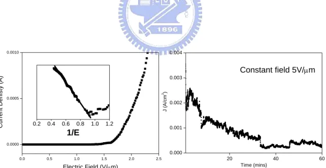
graphite………..40 Fig. 3.6 Schematic diagram of micro-Raman equipment………40 Fig. 3.7 Schematic diagram of field emission measurement setup……….41 Fig. 4.1 SEM images of carbon nanotubes: (a) Cross-section view (b) Magnified view…...44 Fig. 4.2 TEM image of the carbon nanotube; (a) the fish bone body and (b) the catalyst on the tip……….44 Fig. 4.3 Raman spectrum of carbon nanotubes grow at different H2 and CH4 flow………..45
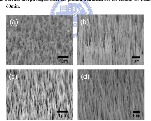
Fig. 4.4 Field emission measurement of carbon nanotubes. (a) I-V measurement and (b) life-time measurement. The inset in (a) is an F-N plot showing field emission behavior……….45 Fig. 4.5 Surface morphologies after H2 plasma treatment for (a) 15min, (b) 30min and (c)
60min……….48 Fig. 4.6 SEM images of carbon nanotubes using Cr as catalyst with different H2 flows; (a)
H2/CH4=20/10, (b) H2/CH4=30/10, (c) H2/CH4=40/10, (d) H2/CH4=50/10……….48
Fig. 4.7 Cross-section SEM images of CNTs grew at different H2/CH4 concentration. (a)
H2/CH4=30/10, (b) H2/CH4=40/10, (c) H2/CH4=50/10………49
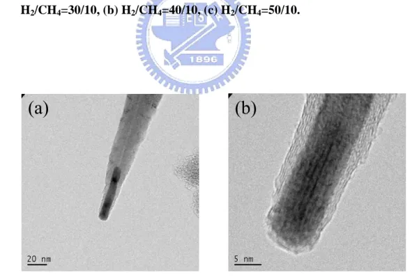
Fig. 4.8 TEM images of CNT grow with Cr. (a) The tip with catalyst on the top with tubular structure and (b) magnified view of the tip………..49 Fig. 4.9 Raman spectrum of (a) different hydrogen to methane flows and (b) correspond ID/IG
ratio………...50 Fig. 4.10 (a) I-V measurement and (b) life-time measurement of CNTs grew by Cr. The inset in (a) is an F-N plot showing field emission behavior………...51 Fig.4.11 Surface morphologies with different film composition of (a) Ni 200Å (b) Ni
150Å ,Au 50Å (c)Ni 130Å , Au 70Å (d)Ni 100Å, Au 100Å , which show different surface roughness. The scale bar in the image is 1µm………..55 Fig. 4.12 SEM images of different density of CNTs (a) 2.2×108cm-2 (b) 6.1×107cm-2 (c)
4.7×107cm-2 (d) 3.3×107 cm-2and the insets show the corresponding cross section images. The scale bar in the image is 1µm………56 Fig.4.13 TEM images of the CNTs showing (a) the curved CNT consist of nickel and gold, (b) straight CNT consist of nickel………56 Fig. 4.14 Field emission from different densities of CNTs shown in Fig. 4.12………57 Fig. 4.15 Plot of field enhancement factors and turn-on fields versus density of CNTs……..57 Fig. 4.16 SEM images of nanostructures with different catalyst amount and composition.
(a)20 nm gold, (b)15 nm gold with 5 nm nickel, (c) 10 nm gold with 10 nm nickel and (d) 5 nm gold with 15 nm nickel………63 Fig. 4.17 Dimension change of the nanostructure shown in Fig 4.16………..63 Fig. 4.18 Effects of annealing temperature on surface morphologies. (a) as deposit film, (b) annealed at 800℃, (c) annealed at 900℃ and (d) annealed at 1000℃……….63 Fig. 4.19 (a) SEM images of octopus-like structures with gold and nickel film thicknesses of 5
and 18nm. (b) TEM image of an octopus-like structure. The inset shows the high-resolution image of the SiONW. The scale bar in the inset represents 20 nm. (c) Elemental analysis of structure by SAM. P1 denotes the catalyst particle, P2 denotes the nanowires and P3 denotes the substrate, respectively………65 Fig.4.20 (a) SEM image of aligned SiONWs. The inset shows the cross-sectional image and the scale bar also represents 5 um. (b) TEM image of aligned SiONW. The insets show the diffraction patterns of the silicon oxide body and catalyst………66 Fig. 4.21 (a) A comb-like SiONW structure and (b) SiONW fill with catalyst inside……….66 Fig. 4.22 Schematic representations of cellular growth stages induced by constitutional
supercooling during rapid solidification………69 Fig. 4.23 Schematic diagram of growth processes of octopus-like and aligned SiONW
structures………69 Fig. 4.24 (a) Low magnification SEM image showing the uniformity of the vertical aligned
chromium carbide capped carbon nanotips and (b) higher magnification top view image……….74 Fig. 4.25 TEM images showing (a) the cross-section view of chromium carbide capped carbon nanotips and, (b) high magnification view of an individual carbon nanotip and the inset shows the chromium carbide head………74 Fig. 4.26 SEM images of surface morphology change with H2/CH4 of (a) 10/10, (b) 30/10, (c) 50/10 and (d) 100/10……….75 Fig. 4.27 SEM images of surface morphologies with applied biases: (a) 100V, (b) 150V, (c) 200V and (d) 300V………75 Fig. 4.28 Ratios of ID/IG with methane concentrations and biases………76
Fig. 4.29 Tip length variation with growth time under applied bias of 150V and 300V……..76 Fig. 4.30 Surface morphologies of chromium carbide capped carbon nanotips with different growth time………77
Fig. 4.31 Schematic diagram of the proposed growth model: (a) formation of the nucleation process; (b) cap growth; (c) deposition of carbon; (d) asparagus-like structure forms………..77 Fig. 4.32 SEM images showing the surface morphology of (a)(b) carbon nanotips and (c)(d)
chromium carbide capped carbon nanotips……….…….…..81 Fig. 4.33 The field emission current density as a function of the electric field for (a) carbon nanotips and (b) chromium carbide capped carbon nanotips. The insets show the Fowler-Nordheim plot for each material………82 Fig. 4.34 Plot of electric field with emission time for carbon nanotips and chromium carbide
capped carbon nanotips. The current was set to a constant value of 1mA…………83 Fig. 4.35 Image of the lighted phosphor in vacuum chamber during field emission
measurement test which is taken by digital camera………...…83 Fig. 4.36 Fabrication process of the gated structure using n+ poly-Si………..86 Fig. 4.37 SEM images of the gated device with n+ poly-Si layer showing (a) carbon deposit on the edge of the poly Si and (b) the poly-Si is etched away in plasma………...86 Fig. 4.38 SEM images of chromium carbide capped carbon nanotips grow in the gated
structure………..87 Fig. 4.39 SEM image of the chromium carbide capped carbon nanotips showing high
alignment………87 Fig. 4.40 SEM images of chromium carbide capped carbon nanotips grow in triode structure with bias of (a) 150V (b) 200V (c) 250V, respectively……….88 Fig. 4.41 Field emission measurements of the gated structure: (a) I-V and (b) F-N plot……89 Fig. 4.42 Selective growth of chromium carbide capped carbon nanotips on planer surface
with gaps of (a) 6µm, (b) 10µm and (c) 20µm………..89 Fig. 4.43 Field emission I-V curves of different carbon nanomaterials………..93 Fig. 4.44 Life-time measurements of CNTs grew from Fe and Cr……….93
Chapter 1 Introduction
1.1 Foreword
With the developments of semiconductor technology, quality of life has been promoted enormously. Consumer products, for example, cell phone, flat panel display, computer, etc., have already become indispensable in our daily life and are vital to global economy. Claims of the consumer products, including light in weight, slim in dimension and efficient in energy consumption are all constantly improved. Most improvement of the mentioned performances come mainly from great developments of fabrication techniques that follow the Moore’s Law[1] which was already a prediction over 40 years ago. The improvements of the semiconductor fabrication techniques will no doubt facing a choke point in the near future. Nanotechnology, defined as the dimension of the material less than 100nm, is the key to the next generation of fabrication techniques.
Wealth of interesting and new phenomena are associate with nanometer-sized structures, with the best established examples including size-dependent excitation or emission[2], quantized (or ballistic) conductance[3], coulomb blockade (or single electron tunneling, SET)
[4], and metal-insulator transition[5]. It is generally accepted that quantum confinement of
electrons by the potential wells of nanometer-sized structures may provide one of the most powerful means to control the electrical, optical, magnetic and thermoelectric properties of a solid-state functional material. Differ from the current fabrication techniques, which are top-down processes,[6] require sophisticated state-of-the-art steps. Instead, a bottom-up process is the spirit of the nanotechnology. Bottom-up (or self-assembly)[7,8] approaches to nanofabrication utilizing chemical or physical energies operating at the nanoscale to assemble basic units into microscopic larger structures. As component size decreases in fabrication, bottom-up technologies provide increasingly important complement to top-down techniques.
electronics[10], catalyst,[11] ceramics,[12] and storage media,[13,14] etc. Among all the consumer products, for example, cell phone, television and signboard, each is equipped with a display. Display technologies may include electronic fabrication (e.g. IC circuits), optical technology (e.g. backlight, polarizer) or plasma technology (PDP) that makes it always a challenging technology. And also the increasingly choosy claims of display, for example, high contrast, high brightness and power efficiency, new generations of displays are ceaselessly produced. Currently, the LCD and PDP dominate the market, but there are plenty of improvements need to be done. An FED has all the advantages of a display except the fabrication process and cost. The key lies in successful synthesis of nano-emitters to meet the field emission and mass-production requirements.
1.2 Motivation
The major study of this thesis is based on field emission device which may be applied to electron source, magnetron or most important, field emission display. Since the discovery of carbon nanotubes, vast efforts were made not only on carbon nanotube itself but all other pure or compound materials. From the first Mo tips, Si tips, and diamond tips, to carbon nanotubes nowadays, performance of each material progresses even better. The basic demands for a field emitter have to be with low work function, high aspect ration and small tip radius. One goal of this thesis is to synthesis new kinds of nanomaterials which are able to fit the requirements.
Besides, in order to achieve particle application, issues of field emission stability, efficiency and device fabrication should also be concerned. Therefore, we put efforts to further improve current nanomaterials as carbon nanotubes, by changing the catalyst used and the surface morphology. To achieve practical applications, we intended to fabricate the gated structure and synthesize nanomaterials inside to investigate the field emission properties.
Chapter 2 Fundamental Theory and Literature Review
2.1 Introduction to Carbon Materials
Carbon is the lightest element in the 4th group elements, which has unique properties comparative with other elements. More then 500,000 compounds are identified, which are greater than the sum of the other elements. Besides organic structure, which is about 80% among the 500,000 compounds, carbon appears in several kinds in nature. Fig. 2.1 shows various atomic structure of carbon. Zero-dimensional carbon, such as fullerence, was identified by Kroto et al.,[15] also lead to the discovery of carbon nanotubes.[16] One-dimensional carbon, such as nanotube discovered by Iijima, exhibit amazing behaviors and attracts a lot of attentions. Two-dimensional carbon, such as graphite, and 3-dimensional carbon, as diamond, bonds in sp2, bonds in sp3, respectively, have already been study widely
and extensively. Carbon has an electronic structure of 1s2 2s2 2p2. The 2s and 2p wave functions are normally hybridized to form 4 degenerate orbitals in a sp3 hybridized atom. These carbon-carbon bonds with high strength, for example, the bond strength of a C-C single bond has a value of 356kjmol-1 compared to a value of 226kjmol-1 for the equivalent Si-Si bond. This makes it possible to form carbon chains of phenomenal lengths, which is a property that allows materials such as carbon fibers to be produced. Since the discovery of carbon nanotubes, unique and novel draw great attentions and efforts in the exploitation of application. Carbon related nanomaterials are considered as the first candidate for nanoscale applications.
In this thesis, application of field emission is the basis point. Therefore, one dimension carbon nanomaterials are concerned to investigate the properties and applications. The following are some introductions to these nanomaterials including carbon nanotubes, carbon nanofibers and carbon nanotips.
Fig. 2.1 Various atomic structure of carbon: fullerence, graphite, diamond, and nanotube.
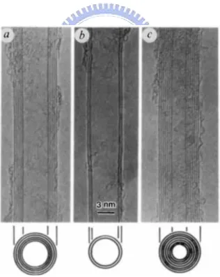
Fig. 2.2 TEM images of CNTs. The parallel lines correspond to the (002) lattice images of graphite. Cross-section images are illustrated in, (a) tube consisting five graphitic sheets with diameter of 6.7nm, (b) tube consisting two graphitic sheets with diameter of 5.5nm and (c) tube consisting seven graphitic sheets with diameter of 6.5nm[16].
2.1.1 Carbon
Nanotubes
Figure 2.2 shows typical electron microscopy images of carbon nanotubes. Since the first observation of multi-wall carbon nanotubes (MWNTs) by Iijima,[16] much attraction has been drawn because of their excellent physical properties and potential applications in various fields. For example, carbon nanotube is probably the best conductor of electricity that can ever be possible.[17-19] Carbon nanotube has comparable thermal conductivity with diamond along the tube axis[20]. With the total area per nanotube bundle for normalizing the applied stress, the calculated Young’s modulous for an individual (10,10) nanotube is ~0.64 TPa.[21] Strong van der Waals attraction leads to spontaneous roping of many nanotubes which is important in certain applications.
The structural and electrical properties of CNTs could be found in articles[22-25] and book.[26-28] A CNT consists of either one cylindrical graphene sheet (Single-walled carbon nanotube, SWCNT) or several nested cylinders with an inter-layer spacing of 0.34 - 0.36 nm (Multi-walled carbon nanotube, MWCNT). Figure 2.3 shows the cutting graphite sheet along the dotted lines which connects two crystalline graphite equivalent sites on a 2-D.[29] The circumference of CNTs can be expressed in term of the chiral vector, Ch, and chiral angle, θ.
The chiral vector is given by Eq. (1):
Ch=na1+ma2≣(n,m) (n, m are integers, 0≦ |m| ≦ n ) (1)
where a1 and a 2 are the primitive vectors length of which are both equal to 3 lC-C, with
lC-C is the length of C-C bond. The chiral angel determines the amount of twist in the tube.
The chiral angles exist two limiting cases that are at 0° and 30°. The chiral angle is defined in Eq. (2) as 2 2 1 1 2 2 cos n m nm m n a C a C h h + + + = ⋅ ⋅ = θ (2) The zig-zag CNT corresponds to the case of m = 0, and the armchair CNT corresponds to
the case of n = m. The chiral CNT corresponds to the other (n, m) chiral vectors. The zig-zag CNT (n, 0) is generated from hexagon with θ= 0°, and armchair CNT (n, n) is formed from hexagon with θ= 30°. The chiral CNT is formed from hexagon with 0°<θ<30°. The inter-atomic spacing of carbon atom is known so that the rolled up vector of CNT can define the CNT diameter. The properties of carbon CNTs depend on the atomic arrangement, diameter, length, and the morphology.[30]
There are many possibilities to form a cylinder with a graphene sheet[33] and a few configurations are shown in Fig. 2.4. Figure 2.4(a)-(c) are SWCNTs of (a) zig-zag, (b) armchair and (c) chiral type. Figure 2.4(d) represents a MWCNT formed by four tubes of increasing diameter with a layer spacing of 0.34 nm. One can roll up the sheet along one of the symmetry axis: this gives either a zig-zag tube, or an armchair tube. It is also possible to roll up the sheet in a direction that differs from a symmetry axis: one obtains a chiral CNT. Besides the chiral angle, the circumference of the cylinder can also be varied.
This diversity of possible configurations is indeed found in practice, and no particular type is preferentially formed. In most cases, the layers of MWCNTs are chiral[31,16] and of different helicities.[32] The lengths of SWCNTs and MWCNTs are usually well over 1 µm and diameters range from ~1 nm (for SWCNTs) to ~50 nm (for MWCNTs). Pristine SWCNTs are usually closed at both ends by fullerene-like halfspheres that contain both pentagons and hexagons.[33]
The electronic properties of SWCNTs have been studied in a large number of theoretical works.[33,34,35-37] These models show that the electronic properties vary in a calculable way from metallic to semiconducting, depending on the tube chirality (n, m) given by[26]
Metallic properties: n-m = 0 or (n-m)/3 = integer Semiconducting properties: (n-m)/3 ≠ integer
The study shows that about 1/3 of SWCNTs are metallic, while the other 2/3 of SWCNT are semiconducting with a band gap inversely proportional to the tube diameter. This is due to
the very unusual band structure of graphene and is absent in systems that can be described with usual free electron theory. Graphene is a zero-gap semiconductor with the energy bands of the p-electrons crossing the Fermi level at the edges of the Brillouin zone, leading to a Fermi surface made of six points.[38] Graphene should show a metallic behavior at room temperature since electrons can easily cross from the valence to the conduction band. However, it behaves as a semi-metal because the electronic density at the Fermi level is quite low. Rolling up the graphene sheet into a cylinder imposes periodic boundary conditions along the circumference and only a limited number of wave vectors are allowed in the direction perpendicular to the tube axis. When such wave vectors cross the edge of the Brillouin zone, and thus the Fermi surface, the CNT is metallic. This is the case for all armchair tubes and for one out of three zigzag and chiral tubes. Otherwise, the band structure of the CNT shows a gap leading to semiconducting behavior, with a band gap that scales approximately with the inverse of the tube radius. Band gaps of 0.4-1eV can be expected for SWCNTs (corresponding to diameters of 1.6-0.6nm). This simple model does not take into account the curvature of the tube which induces hybridization effects for very small tubes and generates a small band gap for most metallic tubes. The exceptions are armchair tubes that remain metallic due to their high symmetry.
These theoretical predictions made in 1992 were confirmed in 1998 by scanning tunneling spectroscopy.[39,40] The scanning tunneling microscope has since then been used to image the atomic structure of SWCNTs,[41,42] the electron wave function[43] and to characterize the band structure.[44] Numerous conductivity experiments on SWCNTs and MWCNTs yielded additional information.[45-56] At low temperatures, SWCNTs behave as coherent quantum wires where the conduction occurs through discrete electron states over large distances. Transport measurements revealed that metallic SWCNTs show extremely long coherence lengths.[56,57] MWCNTs show also these effects despite their larger diameter and multiple shells.[58,59]
Fig. 2.3 Schematic diagram showing how a hexagonal sheet of graphite is rolled to form a CNT[29].
(b) (a)
Fig. 2.5 Structure of carbon nanofibers and nanotubes. (a) stacked cone sherringboned nanofiber and (b) nanotube[68].
(b)
(a)
Fig. 2.6 (a) SEM image of carbon nanofiber and (b) TEM image of an individual carbon nanofiber[66].
2.1.2 Carbon Nanofibers
[61]It has been known for over a century that filamentous carbon can be formed by the catalytic decomposition of carbon-containing gas on a hot metal surface. In a U.S. Patent published in 1889,[62] it is reported that carbon filaments are grown from carbon-containing gases using an iron crucible. In the current literature, the term “nanofiber” is preferentially used, featuring distinction in size scale, while in the past simply “filamentous carbon,” “carbon filaments,” and “carbon whiskers” were applied.[63] In 1985 a form of carbon, buckminsterfullerene C60, was observed by a team headed by Kroto et al.,[64] which led to the
Nobel Prize in chemistry in 1997. This discovery was followed by Iijima’s[16] demonstration in 1991 that carbon nanotubes are formed during arc-discharge synthesis of C60 and other fullerenes, triggering a deluge of interest in carbon nanofibers and nanotubes. In the 1990s the introduction of catalytic plasma-enhanced chemical vapor deposition (C-PECVD) provided additional control mechanisms over the growth of carbon nanostructures. In 1997 Chen et al. used PECVD for nanofiber synthesis.[65] Their work was followed by the better known work of Ren et al.[66]
Carbon nanofibers (CNFs) are cylindrical or conical structures that have diameters varying from a few to hundreds of nanometers and lengths ranging from less than a micron to millimeters. The internal structure of carbon nanofibers varies and is comprised of different arrangements of modified graphene sheets. A graphene layer can be defined as a hexagonal network of covalently bonded carbon atoms or a single two-dimensional (2D) layer of a three dimensional (3D) graphite. In general, a nanofiber consists of stacked curved graphite layers that form cones [Fig. 2.5(b)] or “cups.”[67,68] The stacked cone structure is often referred to as herringbones or fishboned as their cross-sectional transmission electron micrographs resemble a fish skeleton, while the stacked cups structure is most often referred to as a bamboo type, resembling the compartmentalized structure of a bamboo stem. Currently there is no strict
classification of nanofiber structures. The main distinguishing characteristic of nanofibers from nanotubes is the stacking of graphene sheets of varying shapes.
In comparison to carbon nanotubes, carbon nanofibers appear as rod-like in structure, as shown in Fig. 2.6.[69,70] Several methods are used for synthesizing carbon nanofibers, such as microwave plasma chemical vapor deposition, hot filament chemical vapor deposition, plasma enhanced chemical vapor deposition, etc. Catalyst is usually the essential element for the growth of carbon nanofibers. Gated field emission devices using single carbon nanofiber cathodes has also been reported.[71]
2.1.3 Carbon
Nanotips
A carbon nanotip has a solid carbon structure which may be ether amorphous or graphite. Compare to its root part, the diameter of its head is much smaller and normally less than 10nm. Both amorphous carbon and graphite are considered conducting metallically;[72] therefore, combine with its small radii, it is suitable for applications as field emitters.[73] Other applications such as scanning probe microscope tips and nano indenters[74] are also proposed mainly due to the chemical inertness of the carbon surface, and much higher bending stiffness compared to carbon nanotubes.
Different growth methods for fabricating carbon nanotips may include electron–beam -induced deposition (EBID),[75-77] chemical vapor deposition (CVD),[78–80] and plasma-enhanced chemical deposition (PECVD).[81] In our previous work, well aligned carbon nanotips are grown on both bare silicon and platinum film by microwave plasma chemical vapor deposition.[82-83] Generally, the growth of carbon nanotips needs no catalyst, so the top of the tip is only amorphous carbon or graphite. Fig. 2.7 (a) shows SEM plane view image of carbon nanotips, the tip angle is 29°. Fig. 2.7(b) shows TEM image of a single carbon nanotip, the image shows a sharp tip of graphite structure. Fig. 2.7(c) shows the field emission behavior that turns on at low electric field.
(c)
(a)
(b)
Fig. 2.7 (a) top-view of SEM image of carbon nanotips, (b) a single carbon nanotip TEM image and (c) field emission property of carbon nanotips[83].
2.2 Methods for Synthesizing Carbon Materials
Arc Discharge
Arc discharge is the first and the effective way to produce single-wall carbon nanotubes (SWNTs) and multi-wall carbon nanotubes (MWNTs).[84-86] The arc discharge equipment contains a stainless steal vacuum chamber with about 500 torr pressure filled with Helium. Two separated graphite electrode are biased with high current density (50~150A) to about 25~40V. Arc is then induced, and the graphite target is vaporized. Products are deposited on cathode or chamber which includes fullerence, tubes, nano particles and amorphous carbon, etc. Impurities are one of its disadvantages, which need further purifications. Figure 2.8 shows schematic diagram of typical arc discharge equipment.[87]
Laser Ablation
Smalley et al.[88,89] discovered that single-wall carbon nanotubes can be produced by laser ablation with good quality and efficiency, which draws a lot of attention. A carbon target is evaporated by high power continuous CO2 laser or pulse Nd:YAG laser source. The
evaporated species are carried out by Argon or Helium to the water-cooled copper finger or copper wire; single-wall nanotubes are then formed. One specialty is that no amorphous carbon is formed on nanotubes. It has to be noted that, fullerence and multi-wall nanotubes can also be obtained by this method. Fig. 2.9[90] shows schematic diagram of laser ablation equipment.
Fig. 2.8 Schematic diagram of arc discharge equipment (Krätschmer-Huffmann).
Chemical Vapor Deposition (CVD)
Chemical vapor deposition includes thermal CVD, Hot filament CVD, microwave plasma CVD, etc. Catalysts are normally used for the growth of carbon related material. Typically chemical vapor deposition are used for the production of carbon fibers.[91,92] It is not until 1993 that Yacaman et. al.[93] successfully use chemical vapor deposition to deposit carbon nanotubes. And till 1997 microwave plasma enhanced chemical vapor deposition is used to deposit carbon nanofibers and carbon nanotubes.[94,95] Hydrocarbon gases are usually mixed with hydrogen (or ammonia) to be the reaction gas.[96] Products may be carbon nanotubes, amorphous carbon, carbon fiber, or even carbon nano tips, which are correlated to growth temperature, flow rate, reaction gas, growth time, bias, and catalyst. Compare with the methods above, CVD has the advantage of low process temperature, relative good uniformity, convenience, large area growth, and easy for in-situ doping.[97]
Bias Assisted Microwave Plasma Chemical Vapor Deposition (MPCVD)
Microwave plasma chemical vapor deposition is one of the important facilities for thin film deposition, micro manufacturing, and surface treatment.[98] By the advantage of high ion density, high degree of dissociation, high reactivity, and low process temperature, a lot of kinds of substrates are capable of fabrication under low temperature with deposition and etching, which is meaningful for LSI process, microelectronic device, optoelectronic device, polymer, and thin film sensor.
By applying electric field, the reaction gas breakdown to induce electrons and ions. With electromagnetic field obtained by microwave or RF power, more electrons and ions are generated by colliding with the un-dissociated gas. Stable plasma is reached when the generation rate and consumption rate are equal for all species. Unlike traditional thermal plasma, temperature of electrons, ions, and neutral particles in low temperature plasma induced by discharge are not identical. The temperature of electron is about 1000oK, while the
ions and neutral ones are below 500oK. Therefore, low temperature plasma is a non-equilibrium plasma with not only few ions, electrons, but also excite state, transient state, and free radicals. By manipulating these high energy species, reaction which is hard for steady state species are attainable.
Take diatomic plasma for example, the procedure may appear as followed:
(Ⅰ)Ionization
A
2+
e
−→
A
2++
2
e
− (Ⅱ)Dissociative ionizationA
2+
e
−→
A
++
A
+
2
e
− (Ⅲ)AttachmentA
2+
e
−→
A
2− (Ⅳ)DetachmentA
2−+
e
−→
A
2+
2
e
− (Ⅴ)RecombinationA
2++
e
−→
A
2 (Ⅵ)Atom recombination2
A
•→
A
2*any polyatomic molecule is substituent for mentioned above. (•) stands for free radical.
Basically, microwave plasma chemical vapor deposition does not need any electrode or even heater. But in this thesis, bias plays an important role in the growth of nanomaterials, and also an essential term.
When a DC bias is added on to the substrate, before the ions pass through the plasma sheath area, the movement of the ions do not effect by the collision between the ions, comparatively and statistically. Also means the ions can strike the substrate directly and vertically by the applied field.[99]
2.3 Growth Mechanism for Nanomaterials
Due to huge amount compound and various atomic bonding of carbon, plenty of kinds of methods are used for the growth of carbon related nanomaterials. Each method has its advantages, disadvantages, distinguishing feature, and a range for suitable use. Most of them have been successfully synthesize carbon nanotubes.
The model used for describing the growth of nanomaterials still is an issue because of the difficulty for observation under such extremely small scale. Even though, several mechanisms are brought up to characterize the behavior for the growth. Here we discuss some growth models which are considered to be the major mechanism for nanosize material.
Growth mechanism of various kind of bottom-up nanosize materials are generally considered to be three models: Vapor-Solid (VS) model, Vapor-Liquid-Solid (VLS) model, and recently, Solution-Liquid-Solid (SLS) model. Some modifications[100] have also been published which will not be discussed here.
Vapor-Solid (VS) Model
Figure 2.10 shows an approximately growth model of vapor-solid growth mechanism. The diagram takes the growth of GaN for example. Epitaxial growth can be achieved without catalyst or liquid phase. The sum of thermodynamic surface energy and heat of fusion become the driving force for VS growth. The growth rate of VS is dominated by the rate of atoms or molecules diffusion and rearrangement. Compare with the growth mechanism with catalyst, the VS mechanism has a lower growth rate.
Vapor-Liquid-Solid (VLS) Model
The mechanism[101] was first introduced in the 1960s to explain the growth of silicon whiskers or tubular structures[102]. In this model, growth occurs by precipitation from a
supersaturated liquid-metal-alloy droplet located at the top of whisker, into which silicon atoms are preferentially absorbed from the vapor phase. The similarity between the growth of carbon nanotubes and the VLS model has also been pointed out by Saito et al[103-104] on the basis of their experimental findings for multi-walled nanotube growth in a purely carbon environment (Fig. 2.11). Solid carbon sublimates before it melts at ambient pressure, and therefore these investigators suggested that some other disordered carbon form with high fluidity, possibly induced by ion irradiation, should replace the liquid droplet.
Solid-Liquid-Solid (SLS) Model
Figure 2.12[105] shows diagram of solution-liquid-solid growth mechanism which takes Ⅲ-Ⅴ materials for example. No catalyst is used for solution-phase synthesis. The materials are produced as polycrystalline fibers or near-single-crystal whiskers having width of 10 to 150 nanometers and length of up to several micrometers[106]. This mechanism shows that process analogous to vapor-liquid-solid growth operated at low temperatures, while requirement of a catalyst that melts below the solvent boiling point to be its potential limitation.
Fig. 2.10 Schematic diagram of vapor-solid (VS) growth model.
Fig. 2.11 Schematic diagram of VLS growth mechanism for nanotubes.[103]
2.4 Introduction to Field Emission Theory
The science of field emission began in 1928,[109] when Fowler and Nordheim presented the first quantum mechanical model for describing field induced electron emission from a metallic surface; a model still in use today. In deriving their model, Fowler and Nordheim first assumed that the conduction electrons in the emitting metal are describable as a free-flowing ’electron cloud’ - following Fermi-Dirac statistics -and are bound to the metal by an energy barrier at the surface. Under the influence of a field, these conduction electrons can be induced to tunnel through the barrier into vacuum, producing a field-induced electron emission from the metal surface. The presence of the electric field makes the width of the potential barrier finite and therefore permeable to the electrons. This can be seen in Fig. 2.13 which presents a diagram of the electron potential energy at the surface of a metal. Fowler and Nordheim further assumed that the surface barrier can be approximated with a one dimensional energy function without losing significant accuracy.
Field Emission from Metals
The dashed line in Figure 2.13 shows the shape of the barrier in the absence of an external electric field. The height of the barrier is equal to the work function of the metal, φ, which is defined as the energy required removing an electron from the Fermi level EF of the
metal to a rest position just outside the material (the vacuum level). The solid line in Figure 2.13 corresponds to the shape of the barrier in the presence of the external electric field. As can be seen, in addition to the barrier becoming triangular in shape, the height of the barrier in the presence of the electric field E is smaller, with the lowering given by[107]
2 / 1 0
4
⎟⎟
⎠
⎞
⎜⎜
⎝
⎛
=
∆
πε
φ
eE
(3)Fig. 2.13 Diagram of potential energy of electrons at the surface of a metal[108].
Fig. 2.14 Diagram of the potential energy of electrons at the surface of an n-type semiconductor with field penetrates into the semiconductor interior.[108]
Knowing the shape of the energy barrier, one can calculate the probability of an electron with a given energy tunneling through the barrier. Integrating the probability function multiplied by an electron supply function in the available range of electron energies leads to an expression for the tunneling current density J as a function of the external electric field E. The tunneling current density can be expressed by Eq. (4) which is often referred to as the Fowler-Nordheim equation[109]
⎥
⎦
⎤
⎢
⎣
⎡−
=
(
)
3
)
2
(
8
exp
)
(
8
2 / 3 2 / 1 2 2 3y
v
heE
m
y
t
h
E
e
J
π
φ
φ
π
(4)where y=∆φ/φ with ∆φ given by Eq. (3), h is the Planck's constant, m is the electron mass, and t(y) and v(y) are the Nordheim elliptic functions; to the first approximation t2(y)= 1.1 and v(y) =0.95 - y2. Substituting these approximations in Eq. (4), together with Eq. (3) for y and values for the fundamental constants, one obtains
⎟⎟
⎠
⎞
⎜⎜
⎝
⎛
−
×
⎟⎟
⎠
⎞
⎜⎜
⎝
⎛
×
=
−E
E
J
2 / 3 7 2 / 1 2 6exp
10
.
4
exp
6
.
44
10
10
42
.
1
φ
φ
φ
(5)where J is in units of A cm-2, E is in units of V cm-1 and φ in units of eV. Plotting log (J/E2) vs. 1/E results in a straight line with the slope proportional to the work function value, φ, to the 3/2 power. Eq. (5) applies strictly to temperature equal to 0oK. However, it can be shown that the error involved in the use of the equation for moderate temperatures (300oK) is negligible.[110]
Field Emission From Semiconductors
To a large degree, the theory for electron emission from semiconductors can be derived parallel to the theory for metals. However, special effects are associated with semiconductors due to the state of their surface and the fact that an external field applied to a semiconductor may penetrate to a significant distance into the interior. For the case when the external electric field penetrates into the interior of an n-type semiconductor and the surface states are neglected, log(J/E2) is shown to be a linear function of 1/E[111]. However, in place of the work
function φ in the Fowler-Nordheim equation one needs to substitute a quantity χ-δ, where χ is the electron affinity defined as the energy required for removing an electron from the bottom of the conduction band of the semiconductor to a rest position in the vacuum, and δ denotes the band bending below the Fermi level. These parameters are illustrated in Fig. 2.14. The linear dependence of log(J/E2) on 1/E is expected only if the density of the current flowing through the sample is much smaller than the current limiting density Jlim =enµnE/ε, where µn is
the electron mobility and n is the electron concentration in the bulk of the semiconductor.[112,113] At J≈Jlim, the Fowler-Nordheim character of the relationship J(E)
passes into the Ohm's law (if the dependence of electron mobility on the electric field is neglected) which results in the appearance of the saturation region in the emission current vs. voltage curve.[114] Such saturation regions were observed experimentally for lightly doped n-type semiconductors and for p-type semiconductors.[115,116] Electron emission from semiconductors has been a subject of more recent theoretical considerations which takes into account complications due to electron scattering, surface state density, temperature, and tip curvature.[117-119]
Local Field Enhancement Factor
The Fowler-Nordheim equation predicts that a field of l07 V/cm would be necessary to generate an emission current density of 108A/cm2 from a tungsten tip. However, experimental emission data tends to be on the order of ten to one hundred times greater than the predicted emission current density. Schottky postulated that such an enhancement factor would be due to nanostructures on the tip surface. The geometry of these nanostructures concentrates the applied field locally and so they are locations of high electron concentrations. An example of this effect is shown in Figure 2.15(a). If a voltage is applied across two parallel plates separated by vacuum the field lines will concentrate at small structures, commonly nanometer scale structures.
(a) (b)
E
Fig. 2.15 (a) Local Field Enhancement due to nanostructure and (b) Model for local field enhancement.
Fig. 2.16 (a)Simulation of the equipotential lines of the electrostatic field for tubes of 1 mm height and 2 nm radius, for distances between tubes of 4, 1, and 0.5 mm; along with the corresponding changes of the field enhancement factor ß and emitter density (b), and current density (c) as a function of the distance[120].
The apparent enhancement of the applied field is represented by the ß coefficient, which has been dubbed the “local field enhancement factor”. The local field enhancement can be considered a product of the nanoscale protrusion from the metal surface. The local field enhancement can be similarly produced by other nanostructures. The factor is related to the tip radius, r, and the height, h, of the material and field enhancement can be expressed as (6):
V
E
=
β
(6) To incorporate the local field enhancement factor and the constants into the previous equations, the substitution suggested by equation (6) is made. The simplified Fowler-Nordheim equation becomes:(
B
V
V
A
J
I
=
×
α
=
×
2exp
−
/
)
(7) where(
1/2)
2 6/
exp
10
.
4
/
10
42
.
1
×
×
α
×
β
φ
×
φ
=
−A
(8)β
φ
/
10
44
.
6
×
7×
3/2=
B
(9) Along with the I-V curve, a “Fowler-Nordheim plot” is generally shown for a material. Its linearity clearly illustrates whether or not the non-linear I-V curve can be represented by field emission. If the field emission data is properly described by the Fowler-Nordheim equation, the plot shows a straight line with a projected y-axis intercept of B and slope of A.Screening Effect
The Fowler-Nordheim equation has predicted the field emission behavior for a film or a single emitter (which also include a single emitter in the gated device). However in normal cases, the field emission current does not achieve the predicted value since nanostructures are usually synthesized with massive amount. In fact, for high density films, screening effect reduces the field enhancement that account for the decreased emission current. For films of medium density, there is an ideal compromise between the emitter density and the inter-emitter distance, which is sufficiently large to avoid screening effects. A better control of density and morphology (and hence of the β factors) of the films is thus clearly required for future applications.
In the previous reports[120,121], a predicted inter-emitter distance of about 2 times the height of the CNTs optimizes the emitted current per unit area. Simulation of an ideal density of 2.5x10⁷emitters/cm2, or equivalently to 625 emitters per 50x50 mm2 pixel was obtained.
Introduction to Field Emission Device (Display)
The application of field emission is basically the electron source which may be applied into vacuum tubes, magnetrons, electron guns in TEM or SEM, cold-cathode pressure sensors and displays. Here we focus on the application of display technology which nowadays called field emission display (FED).
Fig. 2.17(a) shows the structure of one form of a FED based on emission of electrons from sharp-tipped cones. The cones are small, and each pixel contains hundreds or thousands of them. Instead of thermo-ionic emission, electrons are released in the high electric field that occurs close to the microscopic tips. The field at the tips is determined by the microscopic geometric and the difference in the voltage between the gate and cathode. After emission, the electrons are accelerated towards a phosphor coated on an optically transparent anode on the opposite substrate. The anode voltage is limited by breakdown between spacers. Since the FED needs no magnetic coils to change the trajectory of the electrons, there’s no need for such a dimension like traditional CRT is. Fig. 2.17(b) demonstrates the dimension difference between a CRT and a FED.
Table 1. shows the power efficiency of the state-of-the-art display technologies which reveals the potential advantage of FED. To date, FEDs are still serious competitors to LCDs and concentrate their most important advantages, such as small thickness (less than 1cm), low power consumption (comparable and even less than LCDs), together with such important feature as high luminance efficiency (>5lm/W), high brightness (300-600cd/m2), perfect linear grayscale, wide view angles, and CRT image quality. At the same time, FEDs have no problems with color convergence and x-rays and magnetic irradiation, which is typical for the conventional CRTs. The FEDs do not require polarizers or backlighting and cannot contain black (dead) pixels, as in the LCD case.
(a) (b)
Fig. 2.17 (a) Schematic diagram of a field emission cell (b) comparison between traditional CRT (left) and FED (right) modules.
Chapter 3 Experimental Details
3.1
Fabrication of Metal-Insulator-Silicon Structure
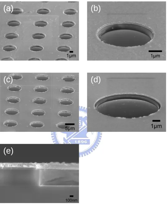
In order to achieve practical application, fabrication of the triode structure (or gated device) is a necessary step prior to the deposition of nanomaterials. Properties of high current density, controllability of emission current, can therefore be attained. Thanks to modern semiconductor technologies, fabricating the triode structure has become facile. There are several ways to fabricate a gated structure and there are vast structures with the same idea have been invented. In this thesis, we fabricate the very original circular triode structure, which was once used to fabricate a Spindt-type structure, to study its characteristics.
Figure 3.1 shows a detail flow chart for fabricating a triode structure. We design a MIS structure and fabricate it by standard semiconductor process technologies. Starting substrate is a polished n-type, (100) oriented wafer with resistivity of 4~6 Ω-cm. The selection of Pt as the electrode has several reasons. First is due to the high melting point that makes it hard to be vaporized and be more resistant to ion-bombardment in the later MPCVD process. Second, the inertia of Pt makes difficult to form compounds. Third, the most important, Pt is relatively hard for the VLS process of carbon that could disturb the selective growth of the nanomaterials. In fact, doped poly silicon has been used to fabricate the structure because of its simplicity in the process steps, but it shows poor resistance that makes it etched away. Therefore, compare with poly silicon, Pt has the fourth advantage, which is good electron conductivity. However, these advantages make the device much complex and require additional steps to fabricate, including several photolithography alignments and lift-off process since Pt is not suitable for reactive ion etching.
All processes for fabricating MIS structure here are supported by National Nano Device Lab and Nano Facility Center, NCTU. The list below shows the model for the fabrication processes.
Photolithography G-line Stepper, ASM PAS2500/10 Stepper Horizontal furnace and LPCVD ASM/LB45 Furnace System
Oxide etcher TEL, TE-5000
Sputtering system ULVAC EBX-10C Dual E-Gun Evaporation System
Clean bench SANTD CLARA PLASTICS Model 1100B
Vertical furnace ASM Vertical Furnace system
1. 6” n-type (100) Si wafer
2. Deposit wet oxide (5800Ǻ) by furnace
3. Photoresist mask by photolithograhy
4. Etch of SiO2 (5800Ǻ) by oxide
etcher
5. Deposit Chromium (200Ǻ) by E-Gun evaporator
6. Removal of photoresist by lift-off process
7. Photoresist mask by photolithography
8. Deposit Titanium (500Ǻ) and Platinum (1500Ǻ) by E-Gun evaporator
9. Remove photoresist by lift-off process
10. Selective growth of Carbon nanotips by BAMPCVD
Si SiO2 PR Cr
Pt Ti Nanotips
(a)
(a)
(b)
(c)
(d)
(e)
Fig. 3.2 SEM images of the triode structure (a) a 50 x 50 array (b) close-view of the array (c) cross-section view (d) an individual hole.
Silicon or silicon coated with catalyst
Deposition of carbon nanomaterials Pretreatment with H2 plasma Fabrication of the gated structure
SEM, TEM Raman, XRD I-V
Characterization of the film and nanostructure
3.2
Deposition of Carbon Nanomaterials by Bias-assisted Microwave
Plasma Chemical Vapor Deposition
Figure 3.3 show approximately the experimental procedure. In most conditions we use two step pretreatments, which include wet cleaning and H2 plasma treatment. The substrates
are first cleaned with organic solvents and washed with de-ionized water with ultrasonic. Pure nitrogen gas is then introduced to dry the substrate before loading into the CVD chamber.
The chamber is evacuated to a pressure of ~10-2 Torr with a rotary pump. To begin the H2
pretreatment process, the reactant gas hydrogen is then introduced into the chamber at a rate of 200 sccm to a setting pressure of 15Torr. The microwave power of 400W is applied and the plasma is obtained. The plasma's horizontal position is adjusted by the plunger to fully immerse the sample in the plasma. The reflected power is minimized to < 10 W with the assistance of a three-stub tuner.
After the hydrogen plasma pretreatment, the reactive gases are introduced into the system by directly changing the mass flow meter. The reactive gases used in deposition are a mixture of CH4 and H2. In order to verified the new material we discovered here, several
parameters are introduced which include H2 plasma pretreatment time, methane concentration,
growth time, and applied bias.
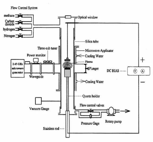
Figure 3.4 schematically depicts the layout of the Bias-assisted MPCVD system. A quartz tube is vertically attached to a rectangular waveguide used as deposition chamber. The microwave from a magnetron source (model IMG 2502-S, IDX Tokyo, Japan) is supplied to the quartz tube through an isolator, three-stub tuner, and a power meter. Then the microwave power is coupled to the quartz tube through an aluminum waveguide with a hole drilled through from top to bottom face. Aluminum tubes extend out from both holes; the tube extensions are water-cooled as well. A sliding short circuit is then attached at the end of the waveguide. The lower position of the quartz tube is connected a stainless steel multi-port chamber equipped with a rotary pump.
The substrates are positioned in the middle of the quartz tube waveguide intersection and held vertically by a substrate holder which is 20mm in diameter, made of molybdenum. Under the holder, attached a tantalum wire which is connected to the bias system; it was used as the lower electrode in the bias treatment stage. A quartz protector under the holder to protect the plasma not attracted to the tantalum wire attached to the molybdenum. The upper electrode, a molybdenum plate of 20mm in diameter which is placed 35 mm above the substrate, also attached to a tantalum wire. The controlled amount of the source gases was introduced into the chamber by mass flow controllers (model 647B, MKS instrument, Inc., USA) from the upper end of the quartz tube. A small window was cut in the waveguide at the center of the plasma cavity, allowing direct observation of the plasma.
In this thesis, nanomaterials including CNTs and carbon nanotips are synthesized with various catalyst and growth parameters. The optimized parameters are listed in Table 3.
Carbon nanotubes Carbon nanotips
Catalyst Fe Cr Ni, Ni/Au Cr Catalyst free
Microwave power 400 W
Operating Pressure 15 Torr
H2 treatment 15 min 30min None
(annealed)
15 min
Gases H2/CH4=40/10 H2/CH4=30/10
Bias None 150V
Growth time 15min 30min
Substrate temperature ~700℃
Fig. 3.4 Schematic diagram of the bias assisted microwave plasma chemical vapor deposition system.
3.3 Analysis Instruments
Scanning Electron Microscopy (SEM)
Scanning electron microscopy is used to observe the surface morphology of wide range kinds of objects. It has the advantage of rather easy sample preparation, high image resolution, large depth of field, and high magnification. A common SEM contains an electron gun to generate electron beams, which will be accelerated under 0.4-40kV voltage. By deflecting the incident beams with the focusing coils, a two dimensional image can be obtained by detect the reflected secondary electrons and the backscatter electrons.
The model we use most here is field emission type SEM JEOL-6500. Accelerating voltage is 15kV with current of 10µA. Working distance is 10mm under 9.63x10⁻⁵Pa.
Transmission Electron Microscopy (TEM)
In a typical TEM a static beam of electrons at 100-400kV accelerating voltage illuminate a region of an electron transparent specimen which is immersed in the objective lens of the microscope. The transmitted and diffracted electrons are recombined by the objective lens to form a diffraction pattern in the back focal plane of that lens and a magnified image of the sample in its image plane. A number of intermediate lenses are used to project either the image or the diffraction patter onto a fluorescent screen for observation. The screen is usually lifted and the image formed on photographic film for recording purposes.
The TEM used for the study is filament type Philips Tecnai-20 equipped with CCD camera for high resolution image.
Raman Spectroscopy
While photons illuminate a molecule or a crystal, they react with the atoms accompany with momentum change or energy exchange. By collecting the scatter photons, we can obtain a sequence of spectrum, including Raman scattering (inelastic scattering) and Reyleigh scattering (elastic scattering). The photon of Raman scattering can be classified into two kinds, Stoke side which photons loss energy or the molecules gains energy, and anti-Stoke side,
which photons gains energy or molecules loss energy. Generally, Stoke side is used to characterize the material. As Raman spectrum provides information of crystallinity and bonding, it has become the most direct and convenient way to identify carbon related materials. The Raman spectrum peak of C-C and C=C bond in crystalline graphite are 1380 (D0peak) and 1580 cm-1(G-peak), respectively, as shown in figure 3.5. The ratio of D-peak intensity (ID) and G-peak intensity (IG), ID/IG is commonly used for characterizing the degree
of graphitization for carbon materials. In a series of test of samples, lower the ratio indicates a better graphitization.[122-124]
The instrument we use is a Renishaw Raman microscope, Model 2000, equipment settings are shown in figure 3.6. The source we use is He-Ne laser with wavelength of 632.82nm and power of 200mW. The spectral slit width is 0.4cm-1.
Field Emission Measurement
A display needs ~0.1 mA/cm2 current density assuming an anode voltage of ~2 kV. The turn-on and threshold field for 10µA/cm2 and 10mA/cm2, respectively have been used as the parameters to characterize various emitter.[125] Fig. 3.7 shows the setup of a field emission measurement facility. To ensure the precision of the gap between the cathode and anode, spacers which are soda-lime glasses with thickness of 150µm are directly attached onto the sample. The anode is an ITO conductive glass with thickness of ~1mm. The length of the field emission area is defined as the distance between the two spacers and the width is the width of the sample itself. High voltage source (Keithley-237) is connected to the anode and cathode by physical contact. The experiment is carried out in a vacuum chamber with pressure of 1x10⁻⁶Torr.
Fig. 3.5 Raman shift of (a) diamond, (b) diamond film, (c) amorphous carbon, (d) graphite.
Anode Spacer Cathode (Emitter)
High voltage source (Keithley 237)
Field emission area HV +
HV
-Vacuum 1x10⁻⁶Torr
![Fig. 2.3 Schematic diagram showing how a hexagonal sheet of graphite is rolled to form a CNT [29]](https://thumb-ap.123doks.com/thumbv2/9libinfo/8410081.179799/22.892.256.715.217.483/fig-schematic-diagram-showing-hexagonal-sheet-graphite-rolled.webp)
![Fig. 2.13 Diagram of potential energy of electrons at the surface of a metal [108] .](https://thumb-ap.123doks.com/thumbv2/9libinfo/8410081.179799/35.892.267.665.202.487/fig-diagram-potential-energy-electrons-surface-metal.webp)