國立交通大學
半導體材料與製程產業研發碩士專班
碩 士 論 文
底膠材料熱機械性質對低介電覆晶球狀陣列封裝體之
熱變形行為研究
The Effect of Underfill Materials’ Thermo-mechanical
Properties on The Thermal Deformation Behavior of
Low-K Flip-Chip Ball Grid Array Packages
研 究 生:陳 欣 源
底膠材料熱機械性質對低介電覆晶球狀陣列封裝體之熱變形行為研究
The Effect of Underfill Materials’ Thermo-mechanical Properties on The Thermal Deformation Behavior of Low-K Flip-Chip Ball Grid Array Packages
研 究 生:陳欣源 Student:Hsin-Yuan Chen 指導教授:呂志鵬 Advisor:Dr. Jihperng (Jim) Leu
國 立 交 通 大 學
半導體材料與製程產業研發碩士專班 碩 士 論 文
A Thesis
Submitted to Industrial Technology R&D Master Program on Semiconductor Materials and Processes
College of Engineering National Chiao Tung University in partial Fulfillment of the Requirements
for the Degree of Master
in
Industrial Technology R&D Master Program on Semiconductor Materials and Processes
August 2008
Hsinchu, Taiwan, Republic of China
底膠材料熱機械性質對低介電覆晶球狀陣列封裝體之熱變形行為研究 學生:陳欣源 指導教授:呂志鵬 博士 國立交通大學半導體材料與製程產業研發碩士專班 摘要 隨著半導體製造技術的發展,積體電路公司引進低介電材料與銅製程用以減 輕電阻電容延遲效應。但是,低介電材料較之傳統的二氧化矽介電質有著較差的 材料機械性質與附著性。這將使得低介電材料層發生破裂的風險大為增加。此 外,由於環保意識的抬頭,無鉛焊料已逐漸取代傳統的錫鉛合金。然而,無鉛焊 料需要更高的迴流溫度(Reflow temperature)以及容易與銅墊產生界金屬化合 物(inter-metallic compounds, IMCs)。這些因素都將降低無鉛焊料覆晶封裝 製程產品的可靠度。因此,針對具有低介電材料的覆晶球狀陣列封裝體,如何調 配其底膠的機械性質以增加其可靠度是目前研發工作的主要課題。
在本研究中,吾人利用高解析雲紋干涉儀去量測並比較二種不同底膠材料的 熱機械變形。該儀器解析度可達 26nm,足以充分觀測底膠與錫球間的熱變形行 為。根據量測的結果,具有較高彈性模數的底膠材料會造成較大的晶片翹曲與較 低的錫球剪應變。此外,我們亦藉由熱循環測試(Thermal Cycling Test, TCT) 評估了包含不同底膠與焊料合金的六種試片之可靠度。測試的結果指出了高鉛焊 料(Sn95Pb)及無鉛焊料(Sn0.7Cu)較傳統的錫鉛共晶焊料(Sn37Pb)可靠度 來的差。因此需要機械性質較強的底膠材料來提供錫球足夠的保護。
另外,我們利用 ANSYSTM
對上述六種試片所預測的應力趨勢亦與熱循環測試實驗有著極佳的相關性。 最後,我們以有限元素分析法來找出應用於低介電覆晶封裝體的最佳底膠機 械性質。底膠的熱膨脹係數、彈性模數與玻態轉換溫度是影響封裝體可靠度的三 大主要因素。根據模擬的結果,較低的底膠熱膨脹係數能同時降低錫球與低介電 層產生裂縫的風險。倘若底膠具有較高的彈性模數,雖然可以提供錫球較佳的保 護,但是將會導致低介電層的應力升高。由於上述二個底膠的材料參數在環境溫 度超過了玻態轉換溫度後會有急遽的變化,因此玻態轉換溫度在底膠的材料性質 中亦扮演一個關鍵的角色。綜上所述,針對低介電覆晶封裝體我們建議使用具有 適中的彈性模數、低熱膨脹係數以及高玻態轉換溫度的底膠材料。
The Effect of Underfill Materials’ Thermo-mechanical Properties on The Thermal Deformation Behavior of Low-K Flip-Chip Ball Grid Array Packages
Student: Hsin-Yuan Chen Advisor: Dr. Jihperng Leu
Industrial Technology R&D Master Program on Semiconductor Materials and Processes
National Chiao Tung University
Abstract
As the advancement of semi-conductor manufacturing technology, the IC manufacturers introduced Cu and low-K dielectric to relieve the resistance-capacitance delay (RC delay) issue. Unfortunately, the low-K dielectric material possessed weaker mechanical strength and adhesion than the traditional SiO2
dielectric, leading to increased delamination potential for low-K layer. In addition, due to the rise of environmental awareness, the conventional eutectic solder alloy Sn37Pb was gradually replaced by lead-free alloys. However, lead-free alloys required higher reflow temperature and the alloys would form Cu-Sn inter-metallic compounds with Cu pads readily, which may degrade the reliability of lead-free packages. Therefore, how to formulate the thermal and mechanical properties of underfill materials to meet the reliability requirements for low-K flip-chip ball grid array (FC-BGA) packages is one of the critical tasks in current research and development of flip-chip technology.
employed to measure and compare the thermo-mechanical deformation of two types of underfill materials. It could provide sufficient sensitivity to observe the thermal deformation behavior in bump/underfill layer. Based on the measurement results, the underfill material with higher elastic modulus induced larger die warpage and lower bump shear strain. In addition, we also evaluated the reliability of six FC-BGA package samples involving different underfill and solder alloys by thermal cycling tests (TCT). The TCT results indicated the package samples with high lead (Sn95Pb) and lead-free bump (Sn0.7Cu) had worse reliability than conventional Sn37Pb bump. Thus, the underfill with more rigid mechanical properties is required in order to protect solder bumps.
Furthermore, a simplified three-dimensional finite element model by ANSYSTM was also established. The die warpage difference between Moiré interferometry measurement and simulation was less than 5%. The stress simulation results by the finite element model also correlated well with aforementioned TCT results.
Finally, finite element analysis (FEA) was employed to find out the optimal mechanical properties of underfill material for low-K FC-BGA packages. The coefficient of thermal expansion (CTE), elastic modulus (E) and glass transition temperature (Tg) of underfill were the three major material properties which directly affected the reliability of FC-BGA packages. Based on FEA results, the underfill with lower CTE would decrease both stress on bumps and low-K layer. For the underfill with higher elastic modulus, it would enhance the bump protection, but induced higher stress in low-K layer. Since CTE and elastic modulus of underfill material would change drastically while environmental temperature exceeded its Tg temperature, Tg temperature was a critical materials property of underfill material. In summary, the underfill material with moderate elastic modulus, low CTE and high Tg temperature was recommended for low-K FC-BGA packages.
Acknowledgements
隨著時光飛逝,終於到了寫致謝詞的時候,這也意味著碩士班的研究生涯即 將劃下句點,而我也將進入人生的下一階段。首先,我要誠摯的感謝我的指導教 授呂志鵬老師在這段時間中悉心的教導。不論是學業或是實驗時所遇到的難題, 亦或是口頭報告時所應注意的事項,甚至是生活細節的瑣事,老師都能不厭其煩 地回答我們的疑問。除此之外,老師還常請我們這些小毛頭去吃好料的、去司馬 庫斯踏青,以及大家一起跑9KM的馬拉松,我想我們一定讓老師破費不少,真是 十分不好意思!但這些回憶的點點滴滴如今想來卻覺得很溫馨很棒。另外,在此 感謝SRC (Semiconductor Research Corporation) 及 UMC Corp. (聯華電子公司) 計畫編號:SRC 2005-KJ1303 所提供的研究經費,還有國家高速網路與計算中心 所提供的計算設施及軟體資源,以及聯華電子公司的陳國明與林宗澍經理提供試 片與實驗建議,使本研究得以順利進行。接著,我要特別謝謝實驗室的國原學長與UT Austin 的Gary學長,沒有了你 們的幫助,我想我不會順利的完成實驗。另外,實驗室的其他好伙伴:幸玲學姊、 宏恩、牧龍、昱涵、明義、泰印、志安學長、鈞元、季高、冠宇同學、少農、王 智、晉誠學弟、怡臻、詩雅以及茹瑛學妹你們大家的幫助與陪伴,我都感念在心。 最後,我要感謝我的家人與女友若穎及愛犬胖胖,謝謝你們一路上的陪伴, 當我遇到論文的瓶頸時,你們的支持與鼓勵讓我有繼續奮鬥的動力,使我能順利 完成碩士學業。 謝誌的結束並不意味著句點,而是人生下一章節的開端。
Contents
摘要 ... Ι Abstract...III Acknowledgements...V Contents ... VI List of Tables ...VII List of Figures ... VIII
Chapter 1 Introduction ...1
Chapter 2 Literature Review...3
2.1 Evolution of IC industry ...3
2.2 Introduction of electronic packaging ...6
2.3 Introduction of flip-chip technology...9
2.3.1 Flip Chip Bumping ... 11
2.3.2 Flip-chip assembly...12
2.4 The challenges in flip-chip packaging technology ...14
2.5 Motivation of this thesis...17
Chapter 3 Experimental Methods ...19
3.1 Moiré interferometry...19
3.1.1 Introduction...19
3.1.2 Theorem of Moiré interferometry...21
3.1.3 Phase shift technique ...31
3.2 Finite Element Analysis (FEA)...33
3.2.1 Introduction to FEA...33
3.2.2 The governing equations for linear elastic material ...34
3.3 Sample preparation for Moiré interferometry...39
3.4 Simulation model and basic assumptions ...43
Chapter 4 Results & Discussion ...46
4.1 Measurement results of regular Moiré interferometry...46
4.2 Comparison between regular Moiré interferometry and simulation...48
4.3 Measurement results of high resolution Moiré interferometry ...51
4.4 Comparison with TCT results and simulation ...65
4.5 The effects of different mechanical properties of underfill ...72
4.6 Mechanical properties of underfill material modification ...75
Chapter 5 Conclusions ...77
List of Tables
Table 1. 1 The melting point for common lead-free solder alloys...2
Table 2. 1 The roadmap of IC manufacture technology ...4
Table 2. 2 IC packaging types...8
Table 2. 3 The comparison among wire bond, TAB, and FC technologies ...9
Table 3. 1 JEDEC precondition level 3...42
Table 3. 2 The dimensions and material properties of the FCBGA assemblies...44
Table 4. 1 The difference between regular Moiré interferometry and simulation ...50
Table 4. 2 TCT1000 results for various packaging samples with different underfill materials and solder bumps...65
List of Figures
Figure 2. 1 The structure of multi-metal layer...3
Figure 2. 2 Gate delay versus technology node ...5
Figure 2. 3 Keff roadmap from ITRS 2007 ...5
Figure 2. 4 Five different levels of electronic packaging. ...7
Figure 2. 5 Flip-chip packaging structure...10
Figure 2. 6 The solder bump manufacturing process by the electro plating method...12
Figure 2. 7 Self-alignment of FC-BGA assembly ...13
Figure 2. 8 Flip-chip assembly process...13
Figure 2. 9 The warpage of FC-BGA assembly...14
Figure 2. 10 The SEM picture of the outmost bump crack after TCT 100 cycles...15
Figure 2. 11 The SEM picture of low-K delamination ...16
Figure 3. 1 The geometry Moiré fringes...20
Figure 3. 2 The schematic diagram of Moiré interferometry...20
Figure 3. 3 The interference phenomenon ...21
Figure 3. 4 The recorded pattern in plane BB...22
Figure 3. 5 (a) A schematic diagram of a grating (b) The SEM picture of the surface of grating. ...23
Figure 3. 6 The diffraction orders of a reflection grating. ...24
Figure 3. 7 The zero and -1 diffraction order when β0 = α, andβ-1 = -α...25
Figure 3. 8 The interference of two intersected coherent beams. ...25
Figure 3. 9 The interference and diffraction on the specimen grating...26
Figure 3. 10 The null field of Moiré interferometry. ...27
Figure 3. 11 The four beams Moiré system ...30
Figure 3. 12 The flow chart of FEA...33
Figure 3. 13 The stress vectors of a 3-D solid. ...35
Figure 3. 14 The experimental FC-BGA assembly (a) before and (b) after cutting ....39
Figure 3. 15 The procedure of sample preparation for Moiré interefermetry...40
Figure 3. 16 (a) The main body of PEMI (b) high-magnification lens...41
Figure 3. 17 The PZT part and its controller ...42
Figure 3. 18 The 3D finite element model. (a) 1/2 symmetry (b) 1/4 symmetry...45
Figure 4. 1 Regular Moiré patterns of (a) U field for UF-1 (b) V field for UF-1 (c) U field for UF-2 (d) U field for UF-2 ...47
Figure 4. 2 The distribution of die warpage for assembly with (a) UF-1 (b) UF-2 ...49
Figure 4. 3 The U field continuous displacement images of the package with underfill-1 (a) Ix1 (b) Ix2 (c) Ix3 (d) Ix4...52
underfill-1 (a) Iy1 (b) Iy2 (c) Iy3 (d) Iy4...53
Figure 4. 5 The phase contour maps of the package with UF-1 (a) U field (b) V field (each fringe spacing = 208nm) ...54
Figure 4. 6 The displacement contour maps of the package with underfill-1 (a) U field (b) V field (each contour spacing = 52 nm) ...55
Figure 4. 7 The U field continuous displacement images of the package with underfill-2 (a) Ix1 (b) Ix2 (c) Ix3 (d) Ix4...56
Figure 4. 8 The U field continuous displacement images of the package with underfill-2 (a) Iy1 (b) Iy2 (c) Iy3 (d) Iy4...57
Figure 4. 9 The phase contour maps of the package with UF-2 (a) U field (b) V field (each fringe spacing = 208nm) ...58
Figure 4. 10 The phase contour maps of the package with underfill-2 (a) U field (b) V field (each contour spacing = 52nm)...59
Figure 4. 11 (a) X direction (b) Y direction displacement alone the three lines in bump/underfill layer ...60
Figure 4. 12 The XY shear strain alone the three lines in bump/underfill layer...62
Figure 4. 13 The displacement measurement by high resolution Moiré interferometry (a) X direction (b) Y direction ...63
Figure 4. 14 The XY plane shear strain results by high resolution Moiré interferometry ...64
Figure 4. 15 The outmost bump stress distribution for sample D (a) XY plane shear stress (b) von Mises stress ...66
Figure 4. 16 The SEM picture of sample D ...67
Figure 4. 17 The max shear stress of the outmost bump ...68
Figure 4. 18 The max von Mises stress of the outmost bump ...68
Figure 4. 19 The σ1 distribution of low-K layer for sample D ...70
Figure 4. 20 The max first principal stress of low-K layer...71
Figure 4. 21 The max stress comparison of different E1 of underfill material for sample E...73
Figure 4. 22 The max stress comparison of different CTE1 of underfill material for sample E...74
Figure 4. 23 Morphology of convential underfill system ...75
Chapter 1 Introduction
In recent years, more and more electronic products appeared in our daily life. High-end electronic products such as microprocessors and graphics chips demanded powerful computing speed and low cost. Hence, the integrated circuits (IC) manufacturers continued scaling the device to enhance the performance and reduce cost. However, device scaling would increase RC delay due to increasing resistance and capacitance. In general, IC manufacturers employed Cu lines and low dielectric constant (low-K) material to relieve the RC delay issue. Unfortunately, the fragile low-K material exhibited a poor adhesion with silicon interface and weaker mechanical properties than traditional SiO2 [1-2], which increased the risk of
delamination between low-K and silicon interface.
Meanwhile, as transistor numbers increased, the packaging assembly needed more pin numbers, shorter connection distance, and more efficient cooling capacity. The flip-chip ball grid array (FC-BGA) packaging technology met aforementioned requirements and has been widely used in high-end electronics package in recent years [3]. However, the large mismatch of coefficient of thermal expansion (CTE) between silicon chip (2.6 ppm/℃) and bismaleimide triazine (BT) substrate (14 ppm/℃) may induce large die warpage and thermal stress during reflow process and thermal fatigue test, resulting in bump crack or low-K delamination. As a result, an underfill layer was introduced between bumps to mitigate the thermal induced stresses and enhance the reliability in the die/package interaction [4-6].
In the solder bumping, tin-lead solder bump is used in traditional bonding process. According to different requirements and processes, tin-lead solder bump could be divided into eutectic alloy, 63Sn37Pb which has a melting point of 183 ℃, and the
high-lead alloy, 95Pb5Sn whose melting point is about 312 ℃. However, lead compounds could infiltrate into the environment with rain water, resulting in the pollution of drinking water and crippling children’s brain development if the electronic products were ineffectively recycled or willfully abandoned. On February 13, 2003, RoHS (Restriction of Use of Hazardous Substances) legislated by European Union required that leaded solder products were restricted to be sold in all Member States after July 1, 2006. In response to EU’s RoHS, manufacturers had invested tremendously in the development of lead-free solder alloys, whose melting points can be summarized in Table 1.1 [7]. The melting points of common lead-free alloys are 210-227 ℃, higher than the traditional 63Sn37Pb eutectic alloy (183 ℃). The higher reflow temperature may induce thermal reliability issues due to larger ΔT incurred in the reflow and bumping steps. Therefore, how to adjust the thermal and mechanical properties of underfill material to protect fragile low-K layer and solder bumps has become a critical challenge for packaging industry.
This thesis is organized into five chapters as described briefly below: (1) Chapter 1 gives a brief introduction on this thesis.
(2) Chapter 2 describes the literature review of key packaging technologies and motivations of this study.
(3) Chapter 3 illustrates the theorems of Moiré interferometry and finite element analysis, and describes the procedures of sample preparation.
(4) Chapter 4 covers the experimental and simulation results, and discussion. (5) Chapter 5 summarizes the key findings and contributions of this thesis work.
Table 1.1 The melting points for common lead-free solder alloys
Chapter 2 Literature review
2.1 Evolution of IC industry
Due to the requirements of multi-function and high speed computing, more transistors were accommodated in a single chip. As the integrated density increased and device size scaled, 2-3 metal-layers interconnects design in > 0.25 μm node no longer met the requirements of wiring signals and current carrying. Below the 65 nm node, 9-11 metal layers were adapted in the IC design, as illustrated typically by Fig. 2.1 [8].
Moreover, due to the great progress of semiconductor manufacture technology and the demand of cost down, the manufacturers in recent years continued to shrink IC device following the Moore’s Law which stated the number of transistors on a chip would be doubled about every 24 months [9].
Table 2.1 revealed the IC manufacture technology roadmap of near-term years according to ITRS Roadmap [9]. However, the continued shrink of the metal line widths also brought some side-effects. Since the increase of total length of metal circuit by multi-layers design and the reduction of metal line widths which made the total resistance value increased substantially. In addition, the capacitance also increased due to the smaller pitch of metal lines. Therefore, the propagation performance of the chip was limited by interconnect delay for technology beyond 0.25 μm node instead of gate delay, as shown in Fig. 2.2 [10]. Thus, the IC manufacturers employed Cu to replace Al as the metal wiring, and used low-K dielectric material to relieve the increase of the RC delay.
Table 2.1 The roadmap of IC manufacture technology (unit: nm) [9]
Year 2007 2008 2009 2010 2011 2012 2013 2014 2015 DRAM 1/2 M1 pitch 65 57 50 45 40 36 32 28 25 MPU/ASIC 1/2 M1 pitch 68 59 52 45 40 36 32 28 25 Flash Poly Si 54 45 40 36 32 28 25 23 20 MPU
Printed Gate length 42 38 34 30 27 24 21 19 17 MPU
Figure 2.2 Gate delay, interconnect delay and total RC delay versus technology node [10]
Figure 2.3 showed that the trend of effective dielectric constant in ITRS 2007 roadmap [11]. However, the next generation ultra low-K (ULK) dielectric materials (K<2.5) have to introduce porous materials. Unfortunately, the nature material characteristic of porous materials would further degrade material strength and reduce interface adhesion.
2.2 Introduction of electronic packaging
With the development of several generations in electronic industry, the process of IC devices scaled down to the nanometer scale. These sophisticated, brittle IC devices could not sustain any surrounding collided and contamination. Therefore, the electronic packaging technologies were applied to protect IC devices and transmit the signals and current between transistors and mother board. The electronic packaging technology has four major purposes which were described below [12]:
1. to support and protect the IC devices
2. to transmit the signals and supply the power 3. to dissipate the heat
4. to avoid the delay of signal transmission
In fact, a complete electronic product needed to go through several package processes. Usually, the electronic packaging could be divided into five different levels as illustrated in Fig. 2.4 [13].
(1) The zero level packaging:
It involved the IC design and fabrication of chips. (2) The first level packaging:
This step would stick the chip into a packaging module. The circuit connection and sealing was completed at this step. This packaging was also called the chip level packaging.
(3) The second level packaging:
In this packaging, the first level packaging devices were connected to the circuit boards.
(5) The forth level packaging:
In this level packaging, several motherboards were combined to form a complete electronic product.
Figure 2.4 Five different levels of electronic packaging [13]
Different electronic products possessed various shapes and functionalities which resulted in the different demands for packaging technologies and materials.
According to the utilized materials, electronic packaging could be divided into ceramic packaging which had better heat dissipation efficiency and reliability, and plastic packaging which had the advantages of low-cost and a thinner volume.
In addition, electronic packaging could also be classified into Pin-Through-Hole (PTH) packaging and Surface Mount Technology (SMT) packaging by IC devices and circuit boards connection methods. Table 2.2 summarized most of packaging types
Table2.2 IC packaging types
Connect type Pin style Pin appearance Packaging Type Vertical to side
area SIP
Single inline
Zig-zag ZIP Dual inline Parallel to side
area DIP/SK-DIP PTH
Bottom Needle ZIP
Single inline L type SVP L type SOP/TSOP/SSOP I type SOP Dual inline J type SOJ L type QFP/LQFP/TQGP I type QFI J type QFJ Quad inline Electrode bump QFN Pin type PGA SMT
Bottom
2.3 Introduction of flip-chip technology
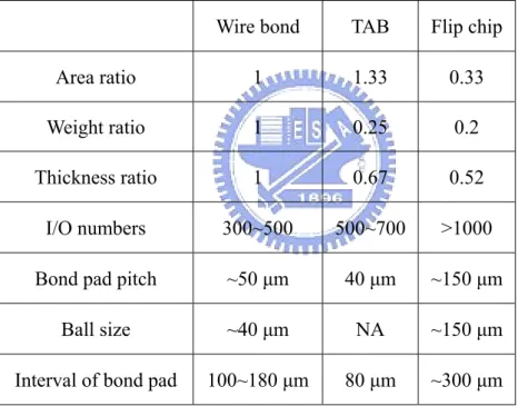
As the advancement of IC industry, the shapes of electric products were requested to be lighter, thinner, shorter, and smaller. These requirements would render more challenges in packaging technology. In general, there are three major methods to accomplish circuit connection, which were wire bonding, tape automated bonding (TAB), and flip-chip (FC) packaging technologies. Table 2.3 summarized the comparison of key features among these three package methods [3].
Table 2.3 The comparison among wire bond, TAB, and FC technologies
Wire bond TAB Flip chip Area ratio 1 1.33 0.33 Weight ratio 1 0.25 0.2 Thickness ratio 1 0.67 0.52
I/O numbers 300~500 500~700 >1000 Bond pad pitch ~50 μm 40 μm ~150 μm
Ball size ~40 μm NA ~150 μm Interval of bond pad 100~180 μm 80 μm ~300 μm
Unlike the wire bonding and TAB packaging, which were peripheral array bonding, the flip-chip packaging employed area array connection. This technology could provide high I/O pins density packaging for high-end electronic products. The flip-chip packaging technology also provided other advantages which were listed as below:
2. lower propagation delay 3. lower self-inductance
4. better heat dissipation and reliability
The flip-chip packaging technology was also called C4 (Controlled Collapse Chip Connection) packaging, when it was proposed by IBM in 1960s [15]. Figure 2.5 showed the basic structure of a flip-chip assembly [16]. The solder bumps were deposited on I/O pads, and then, the chip was flipped and heated to connect with the substrate by molten solder bumps. The flip-chip packaging process could be divided into two steps; namely: flip-chip bumping and flip-chip assembly.
2.3.1 Flip Chip Bumping
The solder bump structure included two parts, which were under bump metallurgy (UBM) and solder ball. The UBM structure usually included three metal layers. The function and materials of each layer were described as below [3]:
1. Adhesion layer:
This layer was employed to enhance the adhesion to bond pads. The main materials of this layer were Ti and Cr.
2. Wetting layer:
The wetting layer increased the adhesion between solders and the adhesion layer. The main materials in this layer were Au, Ag, Cu, and Ni.
3. Protective layer
The main objective of this layer was to protect the Cu or Ni from oxidation. The precious metals like Au, often used in this layer.
The common solder included Sn37Pb eutectic, high lead and lead-free alloys. The solder alloy could be deposited on UBM by evaporation, and electro-plating, and stencil printing. The solder alloy would be melted while the temperature above its melting point, and then formed solder balls after cooling to room temperature. Figure 2.6 illustrated the bumping manufacturing process by electro-plating method [17].
Figure 2.6 The solder bump manufacturing process by the electro plating method [17]
2.3.2 Flip-chip assembly
After the bumping process, the chip had to connect with the substrate to complete the flip-chip assembly. At first, the solder bumps were aligned with the bond pads on the substrate. Afterwards, the assembly was heated and the solder balls would be melted to connect the substrate. During this reflow process, the FC-BGA packaging showed unique self-alignment advantage to avoid bonding failure as shown in Fig. 2.7 [18]. After flux cleaning and underfill dispensing, the package would be heated at about 150 ℃ to cure the underfill material. The role of underfill layer was to protect solder bumps and die from crack and delamination. The major ingredients of underfill included epoxy resin, hardener, catalyst, filler and some additives [3]. The overall process of flip-chip assembly was shown in Fig. 2.8 [19].
Figure 2.7 Self-alignment of FC-BGA assembly [18]
2.4 The challenges in flip-chip packaging technology
The reliability issues of FC-BGA assembly had been of critical concern and closely studied in recent years. Usually, several factors may cause reliability degradation after thermal processing step in flip-chip assembly and thermal cycling test as listed below [20-23]:
1. The inter-metallic compounds (IMC) formation, 2. The CTE mismatch between each material, 3. The thermo-migration behavior, and 4. The electromigration effect.
Due to the CTE mismatch between silicon chip and substrate, the FC-BGA package incurred large warpage as shown in Fig. 2.9. However, the warpage could be mitigated by optimal designs, such as smaller and thinner die, or higher E of thermal interface material (TIM) etc [24].
The silicon chip and organic substrate were connected by solder joints. Therefore, the thermal induced stresses may cause bumps cracks during thermal fatigue tests. Figure 2.10 showed the bump crack occurred at die/solder interface after TCT 100 cycles [25]. H. C. Cheng et al. evaluated the relationship between solder joint fatigue life and die/PCB material properties [26]. Pang et al. also investigated the solder bumps creep phenomenon by simulation [27]. S. K. Groothuis applied non-linear, viscous and plastic properties of solder balls to predict the fatigue life [28].
Figure 2.10 The SEM picture of the outmost bump crack after TCT 100 cycles [25]
In addition, the fragile low-K dielectric layer had high delamination risk due to its weak stiffness and poor adhesion. Figure 2.11 showed the typical delamination at die/low-K interface [29]. K. C. Chang et al. proposed some design guidance for increasing reliability of low-K FC-BGA assemblies [30]. L. Mercado proposed that put some tiles or slots in the interconnect layer to reduce available area for crack growth [31].M. Rasco et al. evaluated the delamination risks of ultra low-K material for different passivation types [32]. L. L. Mercado et al. pointed out that the more Cu
layer of interconnects, the higher risk of low-K delamination [33].This increased the difficulties of FC-BGA for high-end electronic products.
2.5 Motivation of this thesis
As devices continued scaling down to 45 nm node, copper and ultra low-K dielectric materials (k <2.5) has become the mainstream in the backend interconnects for further reduction in RC delay. Since the fragile low-K layer possessed weaker mechanical properties and poor adhesion with silicon chip, the low-K delamination would occur easily than traditional SiO2 dielectric due to the thermal induced stresses
by CTE mismatch between die and BT substrate. In addition, the traditional SnPb eutectic solder was gradually replaced by lead-free solder alloy due to the rise of environmental awareness. The underfill layer played an important role to mitigate the thermal induced stresses from CTE mismatch of each component. Both solder bumps and low-K layer should be protected from cracks and delamination. Therefore, the material properties of underfill should be modified for different FC-BGA packaging applications. Some studies indicated that high modulus and high glass transition temperature were good for bump protection, but increase delamination potential for low-K layer [29, 34].It is difficult to find an optimal underfill material to protect both bumps and low-K layer perfectly due to its opposite requirements in mechanical properties. Thus, how to balance three major material properties (E, CTE and Tg) of underfill materials to protect both bumps and low-K layer becomes a critical challenge for IC packaging industry.
Due to the advancement in simulation programs and computation performance with more powerful computer, the finite element analysis (FEA) had been a popular tool for thermo-mechanical analysis of die/package interaction. The simulation model should be verified by experimental data prior to predictive simulation. The Moiré interferometry had been used to measure the thermal deformation of FC-BGA packages [25, 26, 35]. Unlike regular Moiré interferometry, the high resolution Moiré
interferometry utilized phase shift technology to enhance the resolution to 26 nm. The thermal induced strain in the solder bumps/underfill layer could be measured more exactly by the high resolution Moiré interferometry, which in turn can be used to validate simulation model and results.
In this study, a 3D simulation model using ANSYSTM was first established to analyze the warpage and strain distribution in FC-BGA packages with Sn0.7Cu solder and two latest underfill materials, and validated by experimental results from Moiré interferometry measurement. Such model was then used to analyze the stresses in the bumps and layer-k layer of six FC-BGA package samples with various solder alloys (Sn0.7Cu, Sn95Pb and Sn37Pb) and underfill materials (various E, CTE and Tg) and to compare with reliability results from temperature cycling test (TCT). The impact of various underfill material properties on the stress level at the outmost bump and low-K layer was also addressed in this thesis.
Chapter 3 Experimental Methods
3.1 Moiré interferometry
3.1.1 Introduction
The vocabulary of Moiré is from French whose meaning is a watered silk or mohair fabric. In fact, the Moiré pattern is a common optical phenomenon in our daily life. For example, when light passed through two overlapped combs which have the approximate teeth pitch, we can observe several broad black lines which are called the Moiré fringes as shown in Fig. 3.1 However, there are some conditions need to be met if we want to obtain distinct fringe patterns for science research [36]:
- Equal widths of the bars and spaces - The two gratings are well defined
- The intersection of the two gratings is less than 3 degree - The pitches ratio of the two gratings is less than 1.05
Lord Rayleigh was the first man who employed Moiré fringes to measure object deformation in 1874 [37]. In 1956, J. Guild developed the geometric Moiré by optical interference and diffraction phenomenon [38]. This is the predecessor of Moiré interferometry. In order to achieve highly sensitive measurement, the high frequency grating and coherent light source need to be developed. However, the two key techniques were not mature enough yet, so that Moiré interferometry did not attract much attention in 1950s. The Moiré interferometry has been widely applied in various kinds of deformation measurement until the laser beam and high frequency grating with 1200 lines/mm had been developed in 1980s.
Figure 3.2 showed the schematic diagram of Moiré interferometry. It can provide
interferometry can reach 0.417 μm using a grating with 1200 lines/mm [36]. If we employed the phase-shift technology for Moiré interferometry, the sensitivity could be enhanced to 26 nm [39].
3.1.2 Theorem of Moiré interferometry
[36]
First, we considered two intersected coherent beams as shown in Fig. 3.3. The two laser beams would produce optical constructive and destructive interference in the three-dimensional intersection space. The constructive interference formed some equal spaced relatively high intensity planes. Figure 3.4 revealed the recorded interference image at the cross-section plane (BB) from Fig. 3.3 by a photographic. The adjacent dark and bright bands, namely fringes were observed. The frequency of the fringes, or the fringe gradient on the plane, F, was determined as:
λ
sin
θ
2
1 =
=
G
F
(3.1)Figure 3.4 The recorded pattern in plane BB
The Moiré interferometry needs a diffraction grating to produce Moiré fringes. Figure 3.5 (a) illustrated the cross-line grating which had the same pitch (distance = g) in two orthogonal direction. Figure 3.5 (b) showed the scanning electronic microscope image of a diffraction grating surface with the frequency of 1200 lines/mm. The surface showed regularly spaced bars and furrows to produce optical diffractions. The frequency of a grating (f) means the number of bars per unit length. It often expressed as lines per millimeter or inch. In general, a low frequency grating (f = 10 to 50 lines/mm) is used for geometric Moiré, and a high frequency grating (f = 300 to 2400 lines/mm) is used for Moiré interferometry. The relationship between grating frequency and pitch could be expressed as:
f
g
1
(a)
(b)
Figure 3.5 (a) A schematic diagram of a grating
(b) The SEM picture of the surface of grating
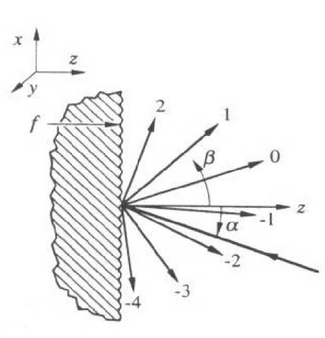
The incident laser beam will be divided into a number of diffracted beams by a reflection grating which was shown as Fig. 3.6. The diffraction angles will follow the grating equation showed as below:
where m is the diffraction order, βm is the angle of the mth diffraction angle, α is
the incident angle, λ is the wavelength, and f is the grating frequency.
Figure 3.7 illustrated a special case while the zeroth diffraction angle is equal to the incident angle α, and -1th diffraction order is -α. Thus, we will obtain the following equation by substituting β-1 = -α to Eq. (3.3).
sin
2
f
λ
α
=
(3.4)Figure 3.7 The zero and -1 diffraction order when β0 = α, andβ-1 = -α
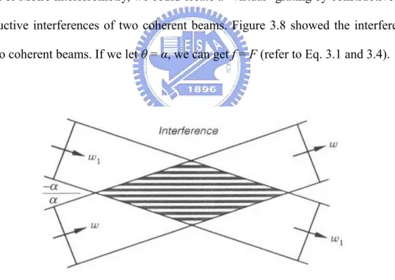
For Moiré interferometry, we could create a “virtual” grating by constructive and destructive interferences of two coherent beams. Figure 3.8 showed the interference of two coherent beams. If we let θ = α, we can get f = F (refer to Eq. 3.1 and 3.4).
Figure 3.8 The interference of two intersected coherent beams
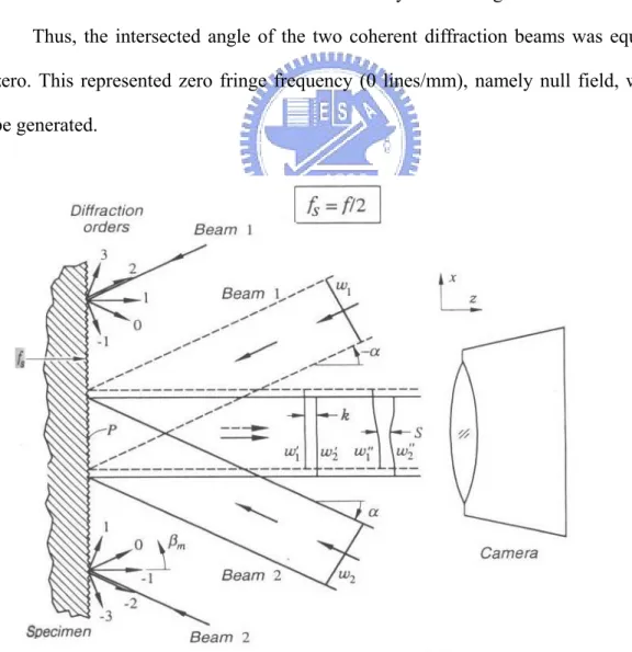
The Moiré interferometry used both interference and diffraction phenomenon to measure deformations of an object as shown in Fig. 3.9. The real grating had been attached to the specimen surface with the frequency of fs. The specimen grating will
deform with the specimen. Two coherent beams produce the virtual reference grating which had the frequency of f. The Moiré fringes would be generated by the interaction of the deformed specimen and reference grating. The camera was used to record the fringe patterns. The relationship between f and fs can be expressed as:
s
f
f
=
β
(3.5) where f is the frequency of reference grating, fs is the frequency of specimengrating, and β is an integral number standing for the fringe multiplication factor. In this study, β=2.
Figure 3.9 The interference and diffraction on the specimen grating
Figure 3.10 depicted the diffraction and interference in Moiré interferometry more detail. The specimen grating had been attached to an undeformed specimen. We
sin
β
m= sin
α
+
m
λ
f
s (3.6)If we substitute the following governing conditions for beam 1:m = 1, f = 2fs, and
( )
f2
sin −α =−λ (refer to Eq. 3.4)
We would find that:
0
sin
β
1=
We also obtained the same result for beam 2 by substituting m = -1.
Thus, the intersected angle of the two coherent diffraction beams was equal to zero. This represented zero fringe frequency (0 lines/mm), namely null field, would be generated.
Now, we considered a uniform normal strain (εx) in the X direction due to a force
applied to a specimen. Thus, the new frequency of the specimen should be modified as: x s
f
f
ε
+
=
1
2
/
(3.7)We substituted the Eq. (3.7) to Eq. (3.6) for the 1st diffraction order beam of beam 1:
( ) ( )
xf
ε
λ
α
β
+
+
−
=
1
2
sin
sin
1 By Eq. (3.4):sin
( )
2
f
λ
α
=
−
−
Thus,(
)
x xf
ε
ε
λ
β
+
−
=
1
2
sin
1Since the value of β1 and εx are very small, therefore:
1
2
xf
ε
λ
β
=
−
(3.8)For the -1st diffraction order beam of beam 2, we can also get the similar equation as below:
x
f
ε
λ
The two coherent diffraction beams had an interacted angle of 2β1. We could
substitute sinθ = β1 in Eq. 3.1 due to θ and β1 were very small. Thus, we could find
the following equation as:
x
xx
f
F
=
ε
(3.9)where Fxx was the fringe gradient in the X direction. It could also express as
⎟ ⎠ ⎞ ⎜ ⎝ ⎛ ∂ ∂ x Nx . Since,
⎟
⎠
⎞
⎜
⎝
⎛
∂
∂
=
=
∂
∂
=
x
N
f
f
F
x
u
xx x x1
ε
Therefore, the relationships between fringe order and displacement can be determined as:
(
)
( , )1
,y x x y xN
f
U
=
( )
( , )1
,y y xy xN
f
V
=
(3.10)where U and V are the displacement of U field and V field, respectively Nx and
Ny are the fringe orders of U field and V field, respectively.
The strains could be represented as:
⎟
⎠
⎞
⎜
⎝
⎛
∂
∂
=
∂
∂
=
x
N
f
x
U
x x1
ε
⎟⎟
⎠
⎞
⎜⎜
⎝
⎛
∂
∂
=
∂
∂
=
y
N
f
y
V
y y1
ε
⎟⎟
⎠
⎞
⎜⎜
⎝
⎛
∂
∂
+
∂
∂
=
∂
∂
+
∂
∂
=
x
N
y
N
f
x
V
y
U
x y xy1
γ
(3.11)Figure 3.11 illustrated the four beams Moiré system. The incident laser beam produced two pair diffraction beams by a cross-line grating. These diffraction beams would produce a virtual reference grating with twice frequency of the actual grating. The Moiré fringe pattern would be observed while the specimen grating deform with the specimen by a CCD camera.
3.1.3 Phase shift technique
The resolution of a regular Moiré interferometry depends on the grating frequency. The most common grating frequency for Moiré interferometry is 1200 lines/mm which represents the resolution of 0.417 μm. However, such sensitivity is not enough to measure the deformation of solder bumps. As a result, a phase shifting Moiré interferometry was employed to enhance the resolution to 26 nm. Each fringe spacing is equal to a 2π phase angle difference and 0.417 μm displacement. The unknown phase angle can be extracted from four precisely phase-shifted interference patterns by phase shifting Moiré interferometry. The intensity of the four patterns can be expressed as [39]:
( )
x
y
I
( ) ( )
x
y
I
x
y
[
( )
x
y
]
I
1,
=
0,
+
′
,
cos
φ
,
( )
( ) ( )
( )
⎥⎦
⎤
⎢⎣
⎡
+
′
+
=
2
,
cos
,
,
,
0 2π
φ
x
y
y
x
I
y
x
I
y
x
I
( )
x
y
=
I
( ) ( )
x
y
+
I
′
x
y
[
φ
( )
x
y
+
π
]
I
3,
0,
,
cos
,
( )
( ) ( )
( )
⎥⎦
⎤
⎢⎣
⎡
+
′
+
=
2
3
,
cos
,
,
,
0 4π
φ
x
y
y
x
I
y
x
I
y
x
I
(3.12) where,I0(x,y) and I’(x,y) are the background and periodically varying intensities in the
interference pattern.
ψ(x,y) is the unknown phase angle of the interference pattern at each pixel
location. Each subsequent pattern is obtained by shifting a phase angle of exactly π/2 of the fringe period.
unknown phase angle by the following equation: 3 1 2 4
arctan
I
I
I
I
−
−
=
φ
(3.13)After the phase angle is solved, the continuous displacement of U field can be determined as:
u
π
f
φ
4
=
(3.14)3.2 Finite Element Analysis (FEA)
3.2.1 Introduction to FEA
The term of finite element analysis (FEA) was proposed by Clough in 1960. The conception of FEA is that an actual object can be divided into many elements and nodes which can be general called mesh. Each element should follow basic mechanical formulas which can be expressed as a matrix. Afterwards, some boundary conditions such as loads and constraints will be inputted into the matrix to obtain the displacements and stresses of the element. Thus, FEA is very useful in scientific research and engineering design fields because it has the advantages of economic and efficiency. Basically, the FEA analysis software is developed to solve the aforementioned matrix. Figure 3.12 showed a general flow chart of FEA. However, the simulation results would still have certain unavoidable errors. The error source may be attributed as the following causes [40]:
1. The difference between simulation model and actual body. 2. Un-appropriate finite element numerical analysis.
3. Mechanics concept or software operation mistakes.
Figure 3.12 The flow chart of FEA
Input element type & material
properties
Construct the solid model
Mesh & create elements
Input loads & constraints Solve
matrixes Output the results
as a diagram or chart
3.2.2 The governing equations for linear elastic material
For a three-dimension structural analysis, we chose the displacement (u), strain (ε), and stress (σ) as the unknown values. Figure 3.13 revealed the stress vectors of a 3-D solid.
{
u
xu
yu
z}
u
=
{
ε
xε
yε
zε
xyε
yzε
zx}
ε
=
{
σ
xσ
yσ
zσ
xyσ
yzσ
zx}
σ
=
For linear elastic material, the relationship between strain and stress should obey the Hooke’s law:
[ ]
E
ε
eσ
=
(3.15)where E is elastic matrix.
If we consider a thermo-mechanical deformation:
th e
ε
ε
ε
=
+
(3.16){
x y z xy yz zx}
T
th=
α
α
α
α
α
α
Δ
ε
where εe represents the elastic strain, εth means the thermal strain, and α is the
coefficient of thermal expansion.
T
T
T
=
ref−
Δ
Figure 3.13 The stress vectors of a 3-D solid
From Eq. (3.15) and (3.16), we can get the following equation as:
[ ]
E
ε
thσ
ε
=
−1+
(3.17) where,[ ]
⎥
⎥
⎥
⎥
⎥
⎥
⎥
⎥
⎥
⎥
⎥
⎥
⎥
⎥
⎥
⎦
⎤
⎢
⎢
⎢
⎢
⎢
⎢
⎢
⎢
⎢
⎢
⎢
⎢
⎢
⎢
⎢
⎣
⎡
−
−
−
−
−
−
=
− zx yz xy z y zy x zx z yz y x yx z xz y xy xG
G
G
E
E
E
E
E
E
E
E
E
E
1
0
0
0
0
0
0
1
0
0
0
0
0
0
1
0
0
0
0
0
0
1
0
0
0
1
0
0
0
1
1ν
ν
ν
ν
ν
ν
where, Ex, Ey, Ez represent the elastic modulus in x, y, z direction, respectively, υ
is the Possion’s ratio, and G is the shear modulus.
In elastic deformation region, the relationship between E, υ, and G can be expressed as:
(
+
ν
)
=
1
2
E
G
(3.18)For isotropic materials:
z y x
E
E
E
E
=
=
=
zx yz xyG
G
G
G
=
=
=
xz zy yx zx yz xyν
ν
ν
ν
ν
ν
ν
=
=
=
=
=
=
z y xα
α
α
α
=
=
=
Thus, Eq. (3.17) can be re-written as:
[ ]
E
+
Δ
T
=
−σ
α
ε
1(3.19)
The normal and plane strains can be determined as:
T
E
E
E
z y x x=
−
−
+
α
Δ
σ
ν
σ
ν
σ
ε
T
E
E
E
z y x y=
−
+
−
+
α
Δ
σ
ν
σ
σ
ν
ε
T
E
E
E
z y x z=
−
−
+
+
α
Δ
σ
σ
ν
σ
ν
ε
σ
G
yz yzσ
ε
=
G
zx zxσ
ε
=
(3.20)The principal strain (εp) can be determined as:
(
)
(
)
(
)
0
2
1
2
1
2
1
2
1
2
1
2
1
=
−
−
−
p z yz xz yz p y xy xz xy p xε
ε
ε
ε
ε
ε
ε
ε
ε
ε
ε
ε
[
ε
1ε
2ε
3]
ε
p=
where ε1, ε2, ε3 is the first, second and third principal stress, respectively. And ε1
> ε2 > ε3.
The von Mises strain (εE) can be repressed as:
(
) (
) (
)
[
]
2 1 2 1 3 2 3 2 2 2 12
1
1
1
⎭
⎬
⎫
⎩
⎨
⎧
−
+
−
+
−
+
=
ε
ε
ε
ε
ε
ε
ν
ε
E Ewhere υE is the effective Possion’s ratio.
(
)
(
)
(
−
)
=
0
−
−
p z yz xz yz p y xy xz xy p xσ
σ
σ
σ
σ
σ
σ
σ
σ
σ
σ
σ
[
σ
1σ
2σ
3]
σ
p=
The von Mises stress (σE) can also be repressed as:
(
) (
) (
)
[
]
2 1 2 1 3 2 3 2 2 2 12
1
⎭
⎬
⎫
⎩
⎨
⎧
−
+
−
+
−
=
σ
σ
σ
σ
σ
σ
σ
E3.3 Sample preparation for Moiré interferometry
The exterior of our experimental FC-BGA packaging sample with 40 x 40 mm2 dimensions was shown in Fig. 3.14(a). In this study, the thermal deformation of FC-BGA assemblies with UF-1 and UF-2 were measured and compared by Moiré interferometry. The solder bumps in these samples were Sn0.7Cu alloy with a pitch of 200 μm.
(a) (b)
Figure 3.14 The experimental FC-BGA assembly (a) before and (b) after cutting
The procedure of sample preparation for Moiré interferometry was schematically illustrated in Fig. 3.15 and described in details as below:
1. The samples were cut by a low speed diamond saw and polished with 1200 grid abrasive papers to the cross-section of the first bump row as shown in Fig. 3.13(b).
2. The cross-section image was observed and captured by the optical microscopy for superposition onto high resolution Moiré images.
3. Both the polished assembly and grating were placed in an oven at 85 ℃ as the zero-displacement reference state. A TRA-BondTM F253 epoxy was chosen as the adhesive. The adhesive was spread out smoothly by optical tissues to control the thickness of adhesive. Afterwards, the cross-section
of the assembly was attached to the thin grating in the oven for an hour. 4. The assembly was pried off from the grating mold carefully after curing
process.
Figure 3.15 The procedure of sample preparation for Moiré interferometry
The Portable Engineering Moiré interferometer (PEMI) from IBM Corp. was employed for this study. To achieve sensitivity up to 26 nm, the PEMI system was upgraded to add a piezoelectric transducer (PZT) part to a high-resolution Moiré interferometer. The reference grating was controlled to shift 147 nm (I2), 295 nm (I3),
and 441 nm (I4) relative to I1 image by the PZT. The experimental equipment was
placed on an optical table to avoid the vibration issue. Figures 3.16 and 3.17 showed our high resolution Moiré system and the PZT part, respectively.
The in-plane thermal deformation of assemblies was measured by Moiré interferometry at room temperature (25 ℃). This represented a -60 ℃ thermal loading applied in the assemblies. The reflective mirrors were tune to produce the null field by the original un-deformed grating before the experimental measurement. After
The fringe patterns were captured by a 1.3 M pixel CCD camera with 12-bit grayscale resolution. A program developed by UT-Austin group was used to analyze the four continuous fringe patterns obtained by high resolution Moiré interferometer
[39].
(a)
(b)
Figure 3.17 The PZT part and its controller
In addition, the thermo-mechanical reliability of six kinds of FC-BGA assemblies with different underfill materials and bump alloys were evaluated by thermal fatigue tests. These assemblies underwent the JEDEC level 3 precondition (260 ℃), which described in details in Table 3.1 and TCT 1000 cycles (from -55 to 125 ℃). The thermal reliability test results would compare with those by stress prediction results using FEA.
Table 3.1 JEDEC precondition level 3 JEDEC precondition level 3
Item Test status Time/Cycles
Bake 125 °C 24 Hours
Moisture Soak 60 °C/60%RH 40 Hours IR reflow (Sn37Pb) 240 °C (peak) 3 X
3.4 Simulation model and basic assumptions
A simulation model using ANSYSTM program was employed to predict the die warpage and stress distribution. The dimensions and material properties of key components in this study which were provided by UMC Corp. are listed in Table 3.2. In this study, the finite elements model had to be establish as a 3-D shapes because the square heat sink ring of the FC-BGA packages need to be considered. Since the packaging samples were symmetric assemblies, a 1/2 model was used for the cut assembly as shown in Fig. 3.18 (a). The simulation results will then compare with the measurement results by Moiré interferometry. In addition, a 3-D 1/4 model with boundary conditions was created for full assembly as shown in Fig. 3.18 (b) to predicted the stress distribution for one TCT cycle. To reduce elements and calculation time, only 10 rows of bumps near the sectioned plane were established. The accuracy of 1/2 symmetric model was validated by the experimental data from Moiré. Since the accurate non-linear material properties and adhesion strength of each component were hardly obtained and a great element numbers (~ 300,000) of the 3-D finite elements model, it was difficult to solve non-linear matrices for TCT 1000 cycles. However, the thermal induced stress of one TCT cycle could be used as an index of delamination potential for qualitative analysis. Therefore, a 1/4 model was used to predict the stress distribution after one TCT cycle from 125 to -55 ℃. The maximum stress value in the outmost bump and lower layer would be compared among various samples. The element type solid 185 of AMSYSTM was used in this study. It was defined by eight nodes, and each node has three degrees of freedom (UX, UY and UZ).
In addition, the following assumptions were applied:
2. All interfaces have perfect adhesion to each other.
3. For 1/2 model, the planes at X=0 was fixed in X direction, keypoint K1 was fixed
in all direction and keypoint K2 was fixed in Y direction.
4. For 1/4 model, the original point K0 was fixed in all direction, the planes at X=0,
and Z=0 were set as symmetric boundary.
5. For the 1/4 model, the reference temperature was set as 125 ℃, and analysis temperature was from 125 ℃ cooled down to -55 ℃.
Table 3.2 The dimensions and material properties of the FCBGA assemblies (sources: UMC)
Properties Material
Thickness (mm) Young's Modulus (kg/mm2) CTE(ppm/℃) ν Tg(℃) Die
(16.35*16.35 mm)
0.75 16000 2.8 0.3 -
Underfill 1 E1=826.5, E2=30.6 CTE1=26 CTE2=91
0.35 125 Underfill 2 E1=969, E2=11
CTE1=27
CTE2=92 0.35 100 Underfill 3 E1=800, E2=4.7 CTE1=32 CTE2=102 0.35 80 Underfill 4 E1=700, E2=4.7 CTE1=32
CTE2=110 0.35 70 Sn0.7Cu 2600 22 0.35 - Sn37Pb 2730 23.5 0.35 - Sn95Pb 0.1 2388 29.1 0.35 - BT Core 0.8 2451 X=Y=14, Z=58 0.28 - Heat Sink, Cu Width=4, thick=0.5 12100 16.3 0.3 -
(a)
(b)
Chapter 4 Results and Discussion
4.1 Measurement results by regular Moiré interferometry
Figures 4.1 (a)-(d) showed the interference images of the packages with UF-1 and UF-2 obtained by regular Moiré interferometry. The grating was replicated onto the cross-section of assemblies at 85 ℃, and measured its deformation at 25 ℃ (ΔT = -60 ℃). Each fringe spacing was 0.417 μm. The neutral line was set as a zero deformation reference due to the symmetry of packages. We can readily calculate the relative displacement by counting the number of fringes from the neutral line.
The fringe patterns of U field showed larger compressive strains at the bottom of package and almost zero strain at the top edge of silicon chip. The V field fringe patterns also showed much higher strain gradient at print circuit board than that at silicon chip. It could be attributed to the higher CTE and lower elastic modulus of substrate than silicon chip. It also revealed that the package was under bending after a cooling process. We could observe some zigzag fringes occurrence in substrate region. These zigzag fringes were not caused by the optical noise or operation mistakes during grating replication step, but by the multiple glass epoxy composite PCB.
Based on the Eq. (3.11), i.e. ⎟⎟
⎠ ⎞ ⎜⎜ ⎝ ⎛ ∂ ∂ + ∂ ∂ = x N y N f y x xy 1 γ , the term of x Ny ∂ ∂ implied that the more fringes of Y direction in U field pattern, the larger shear strain was. So was the term of
y Nx
∂ ∂
. From these fringe images, we observed that the fringe gradient increased gradually from the center to the edge of the chip. This represented the maximum shear would occur at the die edge region.
Neutral line (a) (b) (c) (d)
Figure 4.1 Regular Moiré patterns of
(a) U field for UF-1 (b) V field for UF-1 underfill material (c) U field for UF-2 (d) U field for UF-2 underfill material
4.2 Comparison between regular Moiré interferometry and
simulation
In this study, the Moiré interferometry was employed to verify the accuracy of simulation results. The Y direction displacement from the center to the edge of chip, namely die warpage, was shown in Fig. 4.2. The overall packages were bending downward by the negative value of the displacement of Y direction. The assembly with UF-1 showed smaller die warpage (~0.2 μm) than the assembly with UF-2 for a -60 ℃ thermal loading. It could be attributed to lower elastic modulus of UF-1 underfill material. The compliant underfill material absorbed the contraction force induced by the CTE mismatch between silicon chip and plastic substrate. It indicated that the underfill material with higher elastic modulus would induce larger die warpage.
Table 4.1 summarized the difference between regular Moiré interferometry and simulation on the maximum axial displacements for the assemblies with two different underfill materials. The measurement results showed good agreement with simulation data. The error rates of displacement of V field for the assemblies with UF-1 and UF-2 were 4.97% and 4.75%, respectively. For U field, the error rates were less than 3% for the both assemblies.
(a)
(b)
Figure 4.2 The distribution of die warpage for assembly with (a) UF-1 (b) UF-2 underfill materials
0 2 4 6 8 -18 -16 -14 -12 -10 -8 -6 -4 -2 0 2 Displace ment o f Y d irection ( μ m)
Distance to neutral line (μm)
Simulation Moire 0 2 4 6 8 -18 -16 -14 -12 -10 -8 -6 -4 -2 0 2 Disp lace m e nt of Y dir ect ion ( μ m)
Distance to neutral line (μm)
Simulation Moire
Table 4.1 The difference between regular Moiré interferometry and simulation on the maximum axial displacement
Displacement (μm) Assembly with Fringe counts
Moiré Simulation different rate U field 6 2.50 2.43 2.88% UF-1 V field 38.5 16.06 16.90 4.97% U field 6 2.50 2.43 2.88% UF-2 V field 39 16.26 17.07 4.75%
4.3 Measurement results of high resolution Moiré
interferometry
In U field fringe patterns by regular Moiré interferometry, there were only 1-2 fringes in the bump/underfill layer. We could not observe the thermo-mechanical deformation of bumps in detail. The V field fringe patterns by regular Moiré interferometry were similar. Thus, the resolution of regular Moiré interferometry was not enough to measure the thermo-mechanical deformation of solder bumps with 110 μm diameter because the displacement was too small to be resolved. Therefore, a high resolution Moiré interferometry was used. Its spatial resolution was enhanced to 26 nm by phase shifting technology [39]. Such sensitivity would be adequate for resolving the displacement of solder bumps.
Since delaminations or cracks often occurred near die edge, we employed high resolution Moiré interferometry to observe the thermo-mechanical deformation behaviors of the critical region. Figures 4.3 and 4.4 showed the continuous displacement images of U field and V field for the UF-1 package, respectively. The fringes were shifted precisely by the PZT controller. A program developed by Prof. Paul S. Ho’s group at the University of Texas at Austin was employed to calculate and analysis the displacement and strains of the two assemblies [39]. The U and V field images would be transformed to a phase contour map by this program. The cross-sectional SEM image of the assembly was superimposed onto the phase contour maps with the help of the obvious turns at die/underfill interface of the contour maps for relating with their relative positions. Figures 4.5 (a)-(b) showed the phase contour maps for U field and V field, respectively. Each fringe space was equal to 208 nm for the contour maps. The contour resolution in Fig. 4.6 was enhanced to 52 nm to help us to study the distribution of thermal induced strain in bump/underfill layer. Figures
4.7 – 4.10 were relative images of the UF-2 assembly.
Figure 4.3 The U field continuous displacement images of the package with underfill-1
Figure 4.4 The V field continuous displacement images of the package with underfill-1
(a)
(b)
Figure 4.5 The phase contour maps of the package with UF-1 (each fringe spacing = 208nm)
(a)
(b)
Figure 4.6 The displacement contour maps of the package with underfill-1 (each contour spacing = 52 nm)
Figure 4.7 The U field continuous displacement images of the package with UF-2 underfill material
Figure 4.8 The U field continuous displacement images of the package with UF-2 underfill material
![Table 2.1 revealed the IC manufacture technology roadmap of near-term years according to ITRS Roadmap [9]](https://thumb-ap.123doks.com/thumbv2/9libinfo/8435368.181485/15.892.136.802.809.1089/table-revealed-manufacture-technology-roadmap-years-according-roadmap.webp)
![Figure 2.2 Gate delay, interconnect delay and total RC delay versus technology node [10]](https://thumb-ap.123doks.com/thumbv2/9libinfo/8435368.181485/16.892.151.717.122.462/figure-gate-delay-interconnect-delay-total-versus-technology.webp)
![Figure 2.6 The solder bump manufacturing process by the electro plating method [17]](https://thumb-ap.123doks.com/thumbv2/9libinfo/8435368.181485/23.892.141.750.133.351/figure-solder-bump-manufacturing-process-electro-plating-method.webp)
![Figure 2.8 Flip-chip assembly process [19]](https://thumb-ap.123doks.com/thumbv2/9libinfo/8435368.181485/24.892.146.771.549.909/figure-flip-chip-assembly-process.webp)
![Figure 2.9 The warpage of FC-BGA assembly [24]](https://thumb-ap.123doks.com/thumbv2/9libinfo/8435368.181485/25.892.129.748.541.1036/figure-warpage-fc-bga-assembly.webp)