Influence of As on the Morphologies and Optical
Characteristics of GaSb/GaAs Quantum Dots
Chi-Che Tseng, Student Member, IEEE, Shu-Cheng Mai, Wei-Hsun Lin, Student Member, IEEE,
Shung-Yi Wu, Bang-Ying Yu, Shu-Han Chen, Member, IEEE, Shih-Yen Lin, Member, IEEE,
Jing-Jong Shyue, and Meng-Chyi Wu, Senior Member, IEEE
Abstract— The influence of As atoms on the morphologies of
GaSb quantum dots (QDs) is investigated. Without any special treatment, GaSb quantum rings (QRs) are observed in the embedded GaSb layer even when the uncapped layer reveals QD-like morphologies. With intentional As supply after the uncapped GaSb QD deposition, a QD to QR transition is observed. The phenomenon suggests that insufficient Sb atoms on the GaSb QDs would lead to the QD to QR transition as in the case of embedded GaSb layers. With extended Sb soaking time following GaSb deposition, QD structures could be well maintained for the embedded GaSb layers. A light-emitting diode operated at room temperature is fabricated based on the GaSb/GaAs QD structure. Identical peak positions in photoluminescence and electroluminescence (EL) spectra of the device show that type-II GaSb QDs are responsible for the observed EL.
Index Terms— GaSb quantum dots, light-emitting diode. I. INTRODUCTION
I
N the past few decades, low-dimensional nanostructures, such as quantum dots (QDs) and quantum rings (QRs) have played an important role in studies of the basic physics as well as in device applications [1]–[4]. Among all structures, the self-assembled GaSb/GaAs QDs have attracted much attention in recent years. This structure has unique optical properties due to the type II GaSb/GaAs band alignment where strong hole localization is observed [5]–[8]. Another related nanos-tructure based on the GaSb/GaAs material is the GaSb QRs. Unlike InAs QRs, GaSb QRs can be directly formed under different growth conditions by molecular beam epitaxy (MBE) without the annealing procedure following the partial cappingManuscript received June 8, 2010; revised September 16, 2010; accepted October 9, 2010. Date of current version February 24, 2011. This work was supported in part by the National Science Council, Taiwan, under Grant NSC 99-2628-E-001-001 and Grant NSC 99-2911-I-001-010.
C.-C. Tseng, S.-C. Mai, W.-H. Lin, S.-Y. Wu, and M.-C. Wu are with the Institute of Electronics Engineering, National Tsing Hua University, Hsinchu 300, Taiwan (e-mail: [email protected]; [email protected]; [email protected]; [email protected]; mcwu@ ee.nthu.edu.tw).
B.-Y. Yu, S.-H. Chen, and J.-J. Shyue are with the Research Center for Applied Sciences, Academia Sinica, Taipei 11529, Taiwan (e-mail: [email protected]; [email protected]; shyue@ gate.sinica.edu.tw).
S.-Y. Lin is with the Research Center for Applied Sciences, Academia Sinica, Taipei 11529, Taiwan, the Department of Photonics, National Chiao-Tung University, Hsinchu 300, Taiwan, and also with the Institute of Optoelec-tronic Sciences, National Taiwan Ocean University, Keelung 20224, Taiwan (e-mail: [email protected]).
Color versions of one or more of the figures in this paper are available online at http://ieeexplore.ieee.org.
Digital Object Identifier 10.1109/JQE.2010.2089041
of the GaAs layers [3], [9], [10]. The possible mechanisms responsible for this phenomenon are: 1) the strong surface tension that pulls the GaSb QDs radially outward, and 2) the Sb segregation of the embedded GaSb QDs resulting from intense As–Sb exchange. Since GaAs barriers are required to provide the hole confinement and intense As–Sb exchange is expected for the As/Sb interfaces, different morphologies could be observed for GaSb QDs embedded in GaAs layers and exposed to air. Careful treatment of the As/Sb interface is also very critical for good optical and electrical characteristics of the structure.
In this paper, the influence of As atoms on the morphologies of GaSb QDs is investigated. Without any special treatment, GaSb QRs are observed in the embedded GaSb layer even when the uncapped layer reveals QD-like morphologies. The formation of QR structures is attributed to repelled Sb atoms from the QD summits after the intense As–Sb exchange under As exposure. With intentional As supply following the uncapped GaSb QD deposition, a QD to QR transition is observed. This phenomenon suggests that insufficient Sb atoms on GaSb QDs lead to the QD to QR transition as in the case of embedded GaSb layers. With extended Sb soaking time after GaSb deposition, QD structures can be maintained in the embedded GaSb layers. The long Sb soaking procedure also enhances the photoluminescence (PL) intensity of the GaSb QDs such that light-emitting diodes (LEDs) can be fabricated based on this structure.
II. EXPERIMENTS
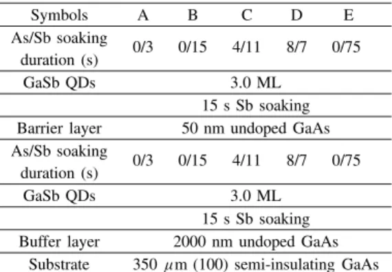
The samples discussed in this paper were grown on (100)-oriented semi-insulating GaAs substrates by a Riber Compact 21 solid-source MBE system. The sample structures are shown in Table I. The 3.0 monolayer (ML) GaSb QDs are grown on the GaAs buffer layers at 490 ºC with a V/III ratio of 2. One sample with a short soaking time (3 s), three samples with different Sb/As soaking times, and the last one with a long soaking time (75 s) were prepared, which are denoted as samples A, B, C, D, and E, respectively. The three samples with different Sb/As soaking time durations are prepared to investigate the influence of As atoms on the morphologies of GaSb QDs. The detailed growth procedure of the three samples are as follows: 1) first, 200-nm GaAs buffer layers are grown at 580 ºC on a GaAs substrate; 2) the substrate temperature is ramped down to 490 ºC in 105 s with the As shutter open to
TABLE I
WAFERSTRUCTURES OFSAMPLESA, B, C, D,ANDE
Symbols A B C D E As/Sb soaking 0/3 0/15 4/11 8/7 0/75 duration (s) GaSb QDs 3.0 ML 15 s Sb soaking Barrier layer 50 nm undoped GaAs As/Sb soaking
0/3 0/15 4/11 8/7 0/75 duration (s)
GaSb QDs 3.0 ML
15 s Sb soaking Buffer layer 2000 nm undoped GaAs
Substrate 350µm (100) semi-insulating GaAs
maintain an As-rich background; 3) the Sb shutter is opened to perform 15 s Sb soaking on the GaAs surface; 4) GaSb QDs of 3.0 ML are deposited on the GaAs buffer layers with a V/III ratio of 2 and the GaSb growth rate is kept at 0.088 µm/h; and 5) different As/Sb soaking time durations of 0/15, 4/11, and 8/7 s are maintained on different samples (which are referred to as samples B, C, and D, respectively). For sample E, the growth procedure is the same as for sample A. The major difference is in the Sb soaking time duration after GaSb deposition.
During QD growth, the reflection high-energy electron diffraction (RHEED) pattern changes from streaks to spots when the GaSb coverage exceeds 2.5 ML, which suggests a 2-D to 3-D growth transition [7]. During the 15 s of Sb soaking procedure before QD deposition, the RHEED pattern quickly changes from that of a (4× 4) surface to a (1 × 3) surface. The phenomenon results from the considerable Sb–As exchange reactions and formation of an Sb-rich surface [11]. This means that ∼1.0 ML GaSb is formed on the surfaces under Sb2-rich background prior to further Ga deposition.
The procedure is to provide an abrupt As/Sb interface for high-quality GaSb QD growth. To investigate the possibility of using the GaSb QDs in LED applications, the single QD structure consists of: 1) a 300-nm p= 2 × 1018 cm−3 GaAs bottom contact layer; 2) a 400-nm undoped GaAs barrier layer; and 3) a 200-nm n = 2 × 1018 cm−3 GaAs top contact layer. The GaSb QD is inserted in the middle of the undoped barrier layer.
Atomic force microscopy (AFM) measurements were car-ried out using a Nanoscope III system (Digital Instruments) to investigate the surface morphology. The cross-sectional trans-verse electron microscopy (TEM) measurement was performed using a JEM-2100F system in high-resolution mode. PL measurements were performed using a Jobin Yvon NanoLog3 system coupled with Xe and tungsten-halogen lamps. For de-vice fabrication, standard photolithography and wet chemical etching were adopted. The device area was of 450×630 µm2. For light extraction, grid top contact was adopted. The positive and negative biases of measurements were defined according to the voltages applied to the top contact of the devices. A Keithley 6487 system was used to measure current–voltage (I–V ) characteristics and acted as the voltage source.
250 nm (a) QD QR 10 nm (b)
Fig. 1. (a) AFM and (b) cross-sectional TEM image of sample A.
III. RESULTS ANDDISCUSSIONS
The 1 × 1 µm2 AFM image of sample A is shown in Fig. 1(a). As seen from the figure, QDs with an average height/diameter 5.7/48 (nm) were observed for the uncapped GaSb layer. The dot density reaches 5.1 × 1010 cm−2. For
InAs/GaAs QDs, although pyramid-shaped QDs would be truncated after GaAs capping, it is generally accepted that the surface morphologies obtained by AFM measurements of the uncapped QDs would be similar to those of the buried dots [12]. However, for InAs/GaAs QDs, there are no group V interfaces as in the case of GaSb/GaAs QDs. The intense As–Sb exchange may lead to different morphologies for the uncapped and buried GaSb QDs. To investigate the phenom-enon, a cross-sectional TEM image of sample A is shown in Fig. 1(b). As seen from the AFM image, GaSb QDs are still visible on the GaAs surface. However, ring-like structures instead of QDs are observed for the buried GaSb layer. These results suggest that, with the GaAs capping layer, the GaSb QDs would transform into QRs. The As–Sb exchange at the GaSb/GaAs interfaces might be playing an important role in this phenomenon.
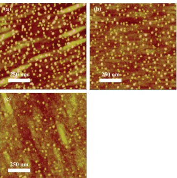
To investigate the influence of As atoms on the GaSb QDs, samples B, C, and D with different Sb/As soaking times were prepared. The AFM images of the three samples are shown in Fig. 2. As seen in Fig. 2(a), QDs are observed for sample B with 15-s Sb soaking. The average QD height, diameter, and density are 2.2 nm, 39.4 nm, and 4.1×1010cm−2, respectively.
As shown in Fig. 2(b) and (c), with the additional As soaking procedure, the QD density decreases. The density of samples C and D are 2.9 × 10¹⁰ and 9.8 × 109 cm−2, respectively. In
250 nm 250 nm
(a) (b)
250 nm (c)
Fig. 2. 1× 1 µm2AFM images of samples (a) B, (b) C, and (c) D.
of ring-like structures are observed in the figures. The densities of the ring-like structures are 3× 10⁹ and 2.2 × 1010 cm−2 for samples C and D, respectively. An interesting phenomenon is that the densities of QDs and QRs for these two samples are both ∼3.2 × 1010 cm−2, which is very close to the dot
density 4.1 × 1010 cm−2 of sample B. These results suggest
that, with As exposure to the GaSb QDs, a QD to QR transition takes place. With increasing As soaking time, the QR density increases.
To explain the phenomenon, a model for the growth dynam-ics is proposed. After GaSb QD deposition, the As soaking procedure induces intense Sb–As exchange on the QD sur-faces. Due to the larger strain on the summits of the QDs, most of the Sb atoms at the summits of QDs would then be repelled from the dots and desorbed to the vacuum chamber [9], [13]. Therefore, with sufficient As soaking or long enough times, the QD structures gradually change to QR structures. Cross-sectional schematic diagrams describing the QR growth evolution are shown in Fig. 3. The phenomenon explains why QR structures are observed for the buried GaSb layer even when QDs are observed for the uncapped GaSb layer.
The results of QR formation after As exposure suggest that, without any special treatment, the buried GaSb layer would tend to form QRs instead of QDs. However, if QD structures are required, a different growth procedure is necessary to maintain the QD morphologies. As described in the last paragraph, the formation of QR structures is attributed to repelled Sb atoms from the QD summits after the intense As–Sb exchange under As exposure. In this case, if sufficient Sb atoms are present on the GaSb surface, the excess Sb atoms may be able to protect the GaSb QDs from the damage caused by the As–Sb exchange. To verify this assumption, sample E with a longer Sb soaking time, i.e., 75 s, after GaSb deposition is prepared. The cross-sectional TEM image of the sample is shown in Fig. 4. As shown in the figure, unlike the case
GaAs GaAs GaAs Sb atom GaSb QDs during Sb Soaking GaSb QDs during As Soaking GaSb QRs after As Soaking As atom
Fig. 3. Cross-sectional schematics describing the QR growth evolution with As exposure.
QD
10 nm
Fig. 4. Cross-section TEM image of sample E.
of sample A, QD structures instead of QRs are observed for the buried GaSb layer. These results confirm the formation mechanisms of ring-like structures observed for the buried GaSb layer of sample A. In this case, without sufficient Sb atoms on the GaSb surfaces, QRs instead of QDs would be obtained. Therefore, to obtain GaSb/GaAs QDs, it is necessary to have a long Sb soaking time after QD deposition to provide excess Sb atoms on the GaSb surfaces so that QD structures could be maintained after GaAs capping layer growth.
Although the embedded QD morphologies are already well maintained by extending the Sb soaking time to 75 s, the PL signals for the five samples are still too weak to measure. A possible reason for this phenomenon may be the defects intro-duced in the Sb/As interfaces while strong As–Sb exchange takes place. In this case, even when the Sb soaking time is long enough to protect the embedded GaSb QD morphologies, the Sb adatoms are still not enough to prevent As–Sb exchange on the interfaces. To improve the optical quality of the GaSb QD structures, another QD sample with similar growth conditions but extending the Sb soaking time to 120 s was prepared with a GaAs p-i-n structure.
The room-temperature PL spectrum of the sample under an excitation power density 0.95 W/cm2 is shown in Fig. 5. As shown in the figure, strong PL intensity is observed for
1.0 1.10 eV P L Intensit y (a. u .)
Photon Energy (eV) RT 0.2 1.080 1.088 1.096 1.104 P L P eak Ener gy (e V ) Power Density (W/cm2) 0.4 0.6 0.8 1.0 1.1 1.2 1.3 1.4 1.5
Fig. 5. Room-temperature PL spectrum of the sample with 120 s soaking time measured at an excitation power density 0.95 W/cm2. The PL peak energies under different excitation power densities are shown in the inset.
RT 1.08 eV EL Intensit y (a. u .)
Photon Energy (eV) −1.8 V (0.68 A/cm2)
1.0 1.1 1.2 1.3
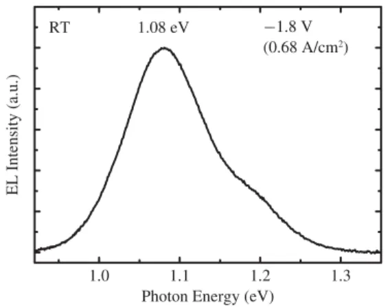
Fig. 6. Room-temperature electroluminescence (EL) spectrum of the LED at−1.8 V. The current density of the device at −1.8 V is 0.68 A/cm2.
the sample, which confirms our previous assumption that by further increasing the Sb soaking time the PL intensity of the GaSb QDs would be enhanced. In this case, the Sb adatoms on the GaSb QDs are sufficient not only to protect the embedded QD morphologies but also to prevent defect formation result-ing from the Sb–As exchange in the GaSb/GaAs interface. Since a strong evidence for the type-II heterostructures is the PL peak blue shift with increasing excitation powers [14], the PL peak energies of the sample under different excitation powers are shown in the inset of Fig. 5. As seen from the figure, on increasing the excitation power density from 0.18 to 0.95 W/cm2, the PL peak position increases from 1.08 to 1.10 eV. This demonstrates that the PL signals are indeed from the GaSb/GaAs QDs.
The EL spectrum of the device at−1.8 V is shown in Fig. 6. As shown in the figure, an EL peak at 1.08 eV is observed for the device, which is close to that under the weak excitation condition of 0.18 W/cm2of the PL spectra. The power density of 0.18 W/cm2 corresponds to 5.74 × 10¹⁷ photons/s· cm2. When the device is at −1.8 V, the current density is 0.68 A/cm2, which corresponds to 4.24 × 10¹⁸ electrons/s · cm2. Assuming that the quantum efficiency is 1.0 for PL, the results suggest that only about 13% of the injected electrons accumulate at the GaSb/GaAs interface and undergo optical re-combination. Otherwise, the EL peak energy should be higher
than the obtained value 1.08 eV, because the peak blue shift should be observed for type-II heterostructures with increasing injection carriers. This also suggests that by allowing the carrier confinement conditions in the device structure, such as replacing GaAs with AlGaAs materials, a better efficiency can be obtained. In this case, GaSb QD LEDs with much higher intensities can be expected in the future.
IV. CONCLUSION
In conclusion, GaSb QRs were observed in the embedded GaSb layer even when the uncapped layer revealed QD-like morphologies. To investigate this phenomenon, intentional As exposure after the uncapped GaSb QD deposition was performed. With the additional As exposure, a QD to QR tran-sition was observed for the uncapped QDs. This phenomenon suggests that the As exposure on the GaSb QDs would lead to a QD to QR transition as in the case of embedded GaSb layers. With extended Sb soaking time (75 s) after GaSb deposition, QD structures could be maintained for the embedded GaSb layers. With even longer Sb soaking time (120 s), strong PL and EL intensities were observed for a GaSb QD p-i-n diode. The results suggest that, with the long Sb soaking procedure, the Sb atoms on the GaSb QDs would prevent the As–Sb exchange and maintain the QD morphology. Therefore, defects resulting from the As–Sb exchange may be gradually eliminated with increasing Sb soaking time. The fabrication of GaSb QDs with good optical characteristics is advantageous for the development of type-II light-emitting devices in the near-infrared range.
REFERENCES
[1] D. Bimberg, M. Grundmann, and N. N. Ledentsov, Quantum Dot Heterostructures. New York: Wiley, 1999, ch. 4.
[2] S.-Y. Lin, W.-H. Lin, C.-C. Tseng, K.-P. Chao, and S.-C. Mai, “Voltage-tunable two-color quantum-dot infrared photodetectors,” Appl. Phys. Lett., vol. 95, no. 12, pp. 123504-1–123504-3, Sep. 2009.
[3] D. Granados and J. M. García, “In(Ga)As self-assembled quantum ring formation by molecular beam epitaxy,” Appl. Phys. Lett., vol. 82, no. 15, pp. 2401–2403, Apr. 2003.
[4] C. L. Tsai, K. Y. Cheng, S. T. Chou, and S. Y. Lin, “InGaAs quantum wire infrared photodetector,” Appl. Phys. Lett., vol. 91, no. 18, pp. 181105-1–181105-3, Oct. 2007.
[5] F. Hatami, M. Grundmann, N. N. Ledentsov, F. Heinrichsdorff, R. Heitz, J. Böhrer, D. Bimberg, S. S. Ruvimov, P. Werner, V. M. Ustinov, P. S. Kop’ev, and Z. I. Alferov, “Carrier dynamics in type-II GaSb/GaAs quantum dots,” Phys. Rev. B, vol. 57, no. 8, pp. 4635–4641, Feb. 1998. [6] M. Hayne, O. Razinkova, S. Bersier, R. Heitz, L. Müller-Kirsch, M. Geller, D. Bimberg, and V. V. Moshchalkov, “Optically induced charging effects in self-assembled GaSb/GaAs quantum dots,” Phys. Rev. B, vol. 70, no. 8, pp. 081302-1–081302-4, Aug. 2004.
[7] K. Suzuki, R. A. Hogg, and Y. Arakawa, “Structural and optical properties of type II GaSb/GaAs self-assembled quantum dots grown by molecular beam epitaxy,” J. Appl. Phys., vol. 85, no. 12, pp. 8349– 8352, Jun. 1999.
[8] C. Jiang and H. Sakaki, “Controlling anisotropy of GaSb(As)/GaAs quantum dots by self-assembled molecular beam epitaxy,” Phys. E, vol. 32, nos. 1–2, pp. 17–20, May 2006.
[9] R. Timm, A. Lenz, H. Eisele, L. Ivanova, M. Dähne, G. Balakrishnan, D. L. Huffaker, I. Farrer, and D. A. Ritchie, “Quantum ring formation and antimony segregation in GaSb/GaAs nanostructures,” J. Vac. Sci. Technol. B, vol. 26, no. 4, pp. 1492–1503, Jul. 2008.
[10] S. Kobayashi, C. Jiang, T. Kawazu, and H. Sakaki, “Self-assembled growth of GaSb type II quantum ring structures,” Jpn. J. Appl. Phys., vol. 43, no. 5, pp. L662–L664, Apr. 2004.
[11] T. Nakai, S. Iwasaki, and K. Yamaguchi, “Control of GaSb/GaAs quantum nanostructures by molecular beam epitaxy,” Jpn. J. Appl. Phys., vol. 43, no. 4, pp. 2122–2124, Apr. 2004.
[12] H. Eisele, A. Lenz, R. Heitz, R. Timm, M. Dähne, Y. Temko, T. Suzuki, and K. Jacobi, “Change of InAs/GaAs quantum dot shape and composition during capping,” J. Appl. Phys., vol. 104, no. 12, pp. 124301-1–124301-5, Dec. 2008.
[13] R. Timm, H. Eisele, A. Lenz, L. Ivanova, G. Balakrishnan, D. L. Huffaker, and M. Dähne, “Self-organized formation of GaSb/GaAs quantum rings,” Phys. Rev. Lett., vol. 101, no. 25, pp. 256101-1–256101-4, Dec. 2008.
[14] D. Alonso-Álvarez, B. Alén, J. M. García, and J. M. Ripalda, “Optical investigation of type II GaSb/GaAs self-assembled quantum dots,” Appl. Phys. Lett., vol. 91, no. 26, pp. 263103-1–263103-3, Dec. 2007.
Chi-Che Tseng (S’08) was born in Taiwan on July 5, 1980. He received the B.S. and M.S. degrees from the Institute of Electrical Engineering, National Taiwan Ocean University, Keelung, Taiwan, in 2006. Since 2006, he has been working toward the Ph.D. degree at the Institute of Electronics Engineering, National Tsing Hua University, Hsinchu, Taiwan.
His current research interests include develop-ment and epitaxy growth of In(Ga)As/GaAs and Ga(As)Sb/GaAs nanostructures and their application to optoelectronic devices.
Shu-Cheng Mai was born in Vietnam on October 16, 1983. He is currently pursuing the Masters degree at the Institute of Electronics Engineering, National Tsing Hua University, Hsinchu, Taiwan.
He is currently in military service.
Wei-Hsun Lin (S’09) was born in Taoyuan, Taiwan, on August 13, 1985. He is currently pursuing the Ph.D. degree at the Institute of Electronics Engi-neering, National Tsing Hua University, Hsinchu, Taiwan.
His current research interests include molecular beam epitaxy and quantum infrared photodetectors.
Shung-Yi Wu was born in Yunlin, Taiwan, on January 8, 1987. He is currently pursuing the Mas-ters degree at the Institute of Electronics Engi-neering, National Tsing Hua University, Hsinchu, Taiwan.
Bang-Ying Yu received the Ph.D. degree from the Department of Material Science and Engineering, National Taiwan University, Taipei, Taiwan.
She is currently with the Chung-Shan Institute of Science and Technology, Taoyuan, Taiwan.
Shu-Han Chen (M’03) was born in Hsinchu, Taiwan, on March 21, 1978. He received the B.S. and Ph.D. degrees in electrical engineering from the National Central University, Taoyuan, Taiwan, in 2000 and 2008, respectively.
He is currently a Post-Doctoral Fellow with the Research Center for Applied Science, Academia Sinica, Taipei, Taiwan. His current research inter-ests include molecular beam epitaxial growth of Sb-based materials and related devices.
Shih-Yen Lin (M’05) was born in Taiwan on November 11, 1972. He received the B.S. degree in physics, and the M.S. and Ph.D. degrees in electrical engineering from National Taiwan Uni-versity, Taipei, Taiwan, in 1995, 1997, and 2001, respectively. His Ph.D thesis was focused on the characteristics of InAs/GaAs quantum-dot structure and its application to infrared photodetectors.
He was a Deputy Manager in the Research and Development Department, Land Mark Optoelectron-ics Corporation, Tainan, Taiwan, from 2001 to 2003. From 2003 to 2006, he was with the Electronics & Optoelectronics Research Laboratories, Industrial Technology Research Institute, Hsinchu, Taiwan. He joined the Research Center for Applied Sciences, Academia Sinica, Taipei, in 2006. He is also an Adjunct Professor in the Department of Photonics, National Chiao-Tung University, Hsinchu, and the Institute of Optoelectronic Sciences, National Taiwan Ocean University, Keelung, Taiwan. His current research interests include applications of nanostructures to optoelectronic devices and molecular beam epitaxy.
Jing-Jong Shyue was born in Taiwan in 1975. He received the B.S. degree in chemistry from National Taiwan University, Taipei, Taiwan, in 1997, and the M.S. and Ph.D. degrees in materials science and engineering from Case Western Reserve University, Cleveland, OH, in 2002 and 2004, respectively. He is now with the Research Center for Applied Sciences, Academia Sinica, Taipei, as an Assistant Research Fellow.
Meng-Chyi Wu (SM’93) was born in Taipei, Taiwan, on November 17, 1957. He received the B.S., M.S., and Ph.D. degrees in electrical engineer-ing from National Cheng Kung University, Tainan, Taiwan, in 1981, 1983, and 1986, respectively.
He was appointed an Associate Professor of elec-trical engineering at National Tsing Hua University, Hsinchu, Taiwan, in 1988, and Full Professor in 1993. His current research interests include organic semiconductor devices and III–V compound semi-conductors, material characterization, optoelectronic devices, epitaxial techniques consisting of liquid-phase epitaxy, metalorganic chemical vapor deposition, and molecular-beam epitaxy.