IEEE TENCON '93 / B e i i n ~
DESIGN & TEST OF MEMORY MANAGEMENT
UNIT AND CACHE CONTROLLER CHIP David Hsieh and Feipei Lai
Dept. of Electrical Eng. National Taiwan University Taipei, Taiwan, China
ABSTRACT
A design and test of memory management unit and cache controller (MMU/CC) chip for the Multiproces- sor Architecture Reconciling Symbolic with numerical processing (MARS are presented in this paper. M- the MARS system for one load per cycle in the absence of cache m i s s , TLB miss, exception or interrupt. Not only the cache and memory operations are supported, but also an invalidation cache coherence protocol is em- bedded. The MMU/CC chip has 66290 transistors and 144 pins. The die size is 8653 p m
*
7114 pm. We take a detailed look at critical issues of the design trade-offs, floor-planning, and testing.INTRODUCTION
MARS is a multiprocessing system, which has a number
of processor board 111. Each processor board is linked together via an interconnection network
,
as depicted in Fig. 1. Inside each board, there are CPU chips, i.e., the instruction fetch unit (IFU) combined with an on- chip instruction cache [2, 31 and the integer processing unit (IPU) 14-61 as well as special chips, the floating- point processing unit (FPU) and the list processing unit (LPU) [7, 81 dedicated for floating point and list opera- tions, external cache for data and instruction along with MMUjCC [9], interleaved global memory, a '32-bit in- struction bus, and a 64-bit d a t a bus whose lower half is time-multiplexed with a 32-bit address bus. Icterleavingmemory into each processor board, instead of a lumped
global shared memory, is t o mainly reduce bus traffic
and the transaction latency[lO-l2]. The MMUjCC of
the MARS system performs the memory operations for both data and instruction requested by other units in the system. MMU/CC handles all of the situations includ- ing a cache-hit, cache-miss, and TLB-miss, excluding a page fault which will cause an interrupt to the system. This chip also supports an invalidation cache coherence protocol for the multiprocessor system.
MU/CC can provi
d
e the memory access requirement ofDESIGN TRADE-OFFS
The virtual memory system of MARS is a paged vir-
tual memory with two-level page tables and page size of
4 kbytes. The virtual space of MARS is partit.ioned into
6
PL'I
I +
h1ur"unNe.d
Fig. 1 Architectural Partitioning of the MARS System
two spaces as shown in Fig. 2, the user space and the system space. The most significant bit, bit 31, is used to specify the addressed region. Each region is given a page table, the system page table (SPT) and the user page table (UPT). User processes are assigned to the user space and all of them share the same system space.
1. Location of Page Tables
If page tables were located flexibly, extra registers are required t o keep the address of page tables. To remove the hardware dedicated for the virtual base registers of
the SPT and the system root page table (SRPT), the
S P T is fixed in the upper region of the system space, ranging from OxffeOOOOO to Oxffffffff, and so is the S-
R P T , from Oxfffff800 to O d f f f f f f . In order not to limit the number of active user processes that can run a t the same time and to remove the virtual base registers for UPT and user root page table (URPT), the UPT and
URPT are also allocated in the precise part of the user
space, from Ox7feOOOOO to Oxi'fffffff and from Ox7fffff800 to Ox7fffffff, respectively.
The system space is further divided into two regions by the bit 30, the mapped and unmapped regions. The data of the unmapped region are also non-cacheable and the purpose to define this region is for running initial- izing programs when the system is booted since a t this
time the contents of page tables, TLB and the caches are
Fig. 2 The Virtual Memory
all invalid. It also removes the need to design a control bit to bypass the TLB and cache for this period.
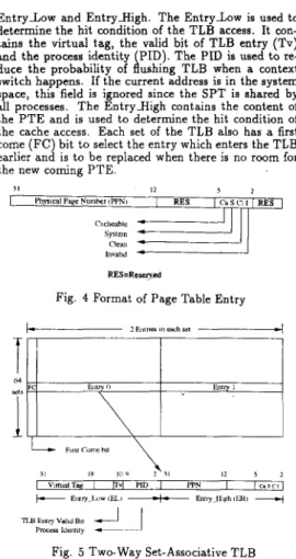
Each virtual address has its own pa e table entry ( P T E ) and root page table entry (RPTEJ. The process of generating the P T E and R P T E of a virtual address, shown in Fig. 3, is very simple. To form the P T E from a virtual address, the most significant bit, system bit, is reserved and the other bits are shifted right ten bits and ten ones are inserted. Since the size of P T E is four bytes and aligned on word boundary, the bottom two bits of the address must be "0". Since the RPTE is practically the PTE's page table entry. The same process is applied to form R P T E from PTE. The P T E of a virtual page, shown in Fig. 4, includes the physical page number (PP-
N) of this page, the cacheable bit (Ca), access control bit S), status bits ( C ) , and invalid bit (I). The reset of Ca [cacheable) bit will cause the cache to be bypassed. The S (System) bit controls the access of the user pro- cess. The operating system can allow a user program t o have access privilege, or no access to a given page.
l l l i l l l l l l
m
I s [
1111111111 I I(I 0Fig. 3 Virtual Addresses of P T E and RPTE The
C
(Clean) bit is used to record whether the page has been modified or not. These bits help the operating system designers reduce the unnecessary T g e swap, and select the victim to be replaced. The I invalid) bit, if reset, indicates that the page exists in the memory.The TLB is two-way set-associative with 128 entries, shown in Fi 5 The hit ratio of this TLB can be high
up to 9 9 . d ; Each entry of TLB includes two parts,
E n t r y L o w and EntryHigh. The EntryLow is used to
determine the hit condition of the TLB access. It con-
tains the virtual tag, the valid bit of TLB entry (Tv)
and the process identity PID) The PID is used t o re-
duce the probability of hushing TLB when a context
switch happens. If the current address is in the system space, this field is ignored since the SPT is shared by all processes. The EntryHigh contains the content of the P T E and is used to determine the hit condition of the cache access. Each set of the TLB also has a first come ( F C ) bit t o select the entry which enters the TLB earlier and is to be replaced when there is no room for the new coming P T E
Caclivible * Cleat1
-
hvalld * RES=Rcsm>Fig. 4 Format of Page Table Entry
b
-
2Entneamearhra4
-TI
I
l
K
Firstf
Come,
hil+
E r ~ n ~ I m v i E l . ~ E n t l y l f ~ e h ~ W ~-
Virtual Ta pm W N C.SCI
'TLEEntly P- ValidBii Identity
A I
----.Fig. 5 Two-way Set-Associative TLB
2. C a c h e Se lec tion
Due t o the lack of on-chip data cache for our unique configuration, the need of a fast external cache excludes the use of physically addressed physically tagged cache (PAPT cache). The three virtually addressed cache or- ganizations that have the same access time are virtually addressed virtually tagged cache (VAVT cache), virtual- ly addressed physically tagged cache (VAPT cache) and virtually addressed dually tagged cache (VADT cache)
(91. We choose the VAPT cache organization because of the following reasons:
A. The constraint of processes sharing is small. The granularity of sharing of two processes is a page. This gives the system better protection.
B. The modification of snooping bus is small. Since the size of cache page number is small, it is easy to be im- plemented by using the non-used signals of commerciai bus.
C. Owing t o the physical tag of this scheme, the re- placed block can be written back immediately without
additional address translation. This simplifies the con- troller design. For the VAVT cache, a physical tag may b e necessary in addition t o virtual tag to prevent possi- ble & d l o c k and to reduce the complexity of controller.
D.
The protection bits, the dirty bit and the process identity are kept in TLB without being duplicated for each cache entry. The separation of the TLB and the cache memory makes the total chip area for memory cells smaller and increases the probability of integrating cache tag and MMU/CC together. Some states of page such as the dirty bit and access bit are easier to support in the TLB than in the cache.E. The memory cells with two read ports can be used to implement the BTag and CTag. They occupy less silicon area than the two tags with only a single read port of the VADT cache and also simplify the tag updating,
In addition to the VAPT scheme, our cache is a write- back, unified cache to reduce the bus traffic, and a direct- mapped cache to match the cycle time of CPU. The cache size is 256 Kbytes and the block size is 32 bytes. An invalidation coherence protocol is adopted for this snooping cache. Exception-b is used by MMUjCC to signal the CPU that a page fault occurs. Fig. 6 shows the timing diagram of an exception. The exception line is precharged at %1 and asserted during 02. The code of exception is presented during 01 of the next cycle through the ad_bus[24:21]. The code of page fault in- cludes a bit t o determine whether this exception is gen-
erated by MMU/CC, a bit to decide which entry of the
two-way TLB is used to detect this fault and two hits for determining the access is for data read, data write, P T E read or R P T E read. In addition, the data address of the page fault is also latched in the bad address register of MMU/CC and accessible by the loadsr instruction.
< W W I "-._,l oi a* i ~ T--DL* U 28 7 l 11 7 . r ~ T U r C - M l a Y M u x c I..d~bY.,>.I1, _* _ _ l p _ Y C r r Y L m ",,61*11ILB *
T'
I
'
*_-".-ldo,.-WI* * ,<.*,ER- X , > w T S R dFig. 6 Exception Timing of Memory Instruction The width of data part of the caches is 2 words (64
bits), If the instruction is to load or store double words, the data is transferred through both the system address bus and the system data bus. If the instruction is to load
or store a single word, the data is transferred through either the system address bus or the system data bus depending on the address hit 2. Only one pair of signals are used to handshake the data transfer. But there are three types of snooping operations and they are writing data to bus, reading data from bus and sending a block to bus for snooping access, respectively. They can he d- ifferentiated by the snooping command sending to/from
the bus controller. At the end of each transfer cycle,
the transfer can be retried if errors are detected. This facilitates the error correction of the received data. The data is sent directly to the cache and the error is detect- ed, then the cache controller is informed after the last transfer.
FLOOR-PLANNING OF MMU/CC
We used GENESIL to design our architecture. Although GENESIL can process the floor-planning and fusion au- tomatically. The designer should not expect to get a good result by these automatic designs. In addition to the constraints of parallel datapaths, one of the prob- lems in the design using GENESIL is the pitch match- ing of different blocks. Lots of silicon area are wasted in the routing of unmatched connections. The sequences and alignments of fusing small modules to make a larger module are also important. A better result will comeout if designers put the size of components, floor-planning and routing into consideration during hierarchically de- composing the function modules.
We consider two serious factors of module position and pad distribution when doing the floor-planning of the
MMU/CC layout
,
shown in Fig. 7. These factors havea great influence on chip performance. The principle of
the first factor is to align modules and assign the priority of routing channels, The area overhead becomes small- er when the principle is obeyed. The principle of the second factor in to put pads in a line, keep the distance from one pad t o the next one equal, and make pads close to the chip core. The area overhead is smaller and so is the delay time when the principle is followed. The equal delay time is crucial since it influences the input delay and output sampling time used in the testing stage.
Fig. 7 MMU/CC Chip Layout
TESTING OF MMU/CC
The MMU/CC chips are tested by usin the test vec- tors generated from the GENESIL simuktor. The sim- ulator simulates a design with functional and switch- level models to verify the design functionality and to generate manufacturing tests. We specify the design
functionality and the netlist, and GENESIL builds the functional simulation models. The simulator uses these models and test vector files or check functions supplied by user, which contain initialization conditions and ad- ditional simulation commands, to verify the operations of the design. The simulator can be controlled directly
on a n interactive screen interface or run in batch. After the layout is specified and compiled, switch-level models are available for design verification. Test vectors, check functions, or both can be used for all simulation of a design. The former can he written in assembly-level or machine-level format. Test vectors evaluate arithmetic and logic expressions easily, but has limited flow-control techniques. Check functions are a series of assertions and verify the design programmatically. They are writ- ten in GENIE using both basic and simulation-specific commands. Test vectors are generated to initial the chip and test all operations. They are not exhaustive since there are more than billion test patterns required in an exhaustive test vector file. Switch-level (GSL) modules are derived from the layout of a GENESIL design and include routing delays. Running the same set of test
vectors successfully on both the GFL (functional) mod-
ule and the GSL module verifies the correspondence of the GFL modules for the initial simulation debugging of a chip design, and with the GSL modules for a final verification of the design and the test vectors, thus the user can shorten the design verification (DV) process in GENESIL. Designers who prefer to do their own design verification should proceed with the switch-level simu- lation after the functional-level simulation.
A bottom-up simulation approach is used to veri- fy the MMU/CC architecture from the blocks up to the chip level hierarchically. We verify the functionali- ty of MMU/CC and simulate every memory operation. We also test every possible situation could happen to a memory access such as cache miss, TLB m i s s , or both. An invalidation cache coherence protocol is also fully implemented to keep the memory system consistent all the t h e . We use test vectors to test the blocks at the bottom level first, then the upper levels, i.e. the gener- al modules are simulated using the check functions. In others words, after the function of the RAM blocks and $he datapath blocks are verified, we test the controller modules individually. Then the large controller module containing the five controllers and the TLB module is proved to work. At last, the whole chip is tested and verified. The critical path of MMU/CC is the MISS signal output to the MARS system. A testing machine provided by IMS is used to test 17 chips and 4 of them
work properly. The clock time of MMU/CC is 200 ns.
CONCLUSION
The MMU/CC chip for the MARS system has been
designed and tested. MMU/CC contains a two-way
set-associative TLB with 64 sets and controls an ex-
ternal cache with 8192 blocks. In the MARS system,
MMUjCC is responsible for all memory operations in our multiprocessor architecture. In each cycle, it can supply a 64-bit data or instruction t o the CPU. The correctness and effectiveness of the MMU/CC chip are verified during the simulation and testing stages.
ACKNOWLEDGEMENT
The work was supported in part by the National Sci- ence Council under Grant NO. 81-0404-E002-121.
REFERENCES
1. jang89-1 G . 3 . Jang, F. Lai, H. C. Lee, Y. C. Maa,
T. M. Parng, and J . Y . Tsai, ”MARS
-
Multiproces- sor Architecture Reconciling Symbolic with Numer-ical Processing,” International Symposzum on VLSI
Technology, System, and Apphcations, May 1989. 2. maa89 Y . 4 . Maa, ”Designing Instruction Fetch U-
nix of the MARS System”, Master Thesis, Computer Science Div., Dept. of Electrical Engineering, Na- tional Taiwan University, 1989.
3. tsai90 W:C. Tsai, ”The Design of Instruction Fet&
Unit for the MARS System”, Master Thesis,
Corn-
puter Science Div., Dept. of Electrical Engineering, National Taiwan University, 1990.
4. jang89-2 G:S. Jang, ”The Design of Integer Pro-
cessing Unit for the MARS System”, Master Thesis, Computer Science Div., Dept. of Electrical Engineer- ing, National Taiwan University, 1989.
5. horng90 C.-J. Horng, ”The Design and Implementa- tion of Integer Processing Unit (IPU) for the MARS System”, Master Thesis, Computer Science Div., Dept. of Electrical Engineering, National Taiwan U- niversity, 1990.
6. chang91 T.-N. Chang, ”The Implementation and Simulation of Integer Processing Unit (IPU) of the MARS System”, Master Thesis, Computer Science Div., Dept. of Electrical Engineering, National Tai- wan University, 1991.
7. tsai89 J.-Y. Tsai, ”The Design of Lisp Processing Unit for the MARS System”, Master Thesis, Com- puter Science Div., Dept. of Electrical Engineering, National Taiwan University, 1989.
8. chen9O C.-Y. Chen ”The Uesign and Implementa- tion of Lisp Processing Unit for the MARS Sys- tem”, Master Thesis, Computer Science Div., Dept. of Electrical Engineering, National Taiwan Univer- 9. sity, wu90 1990. C.-Y. Wu, ” T h e Implementation and Simula- tion of Memory Management Unit and Cache Con- troller for the MARS System”, Master Thesis, Com- puter Science Div., Dept. of Electrical Engineering, National Taiwan University, 1990,
10. tzeng89 L:M. Tzeng ”MARS Performance Evalua-
tion with Different Interconnection Networks”, Mas- ter Thesis, Computer Science Div., Dept. of Electri- cal Engineering, National Taiwan University, 1990. 11. goodman83 J.R. Goodman, ”Using Cache Memory
To Reduce Processor-Memory Traffic”, PTOC. 10th
Symposium on Computer Architecture, 1982, pp.124- 131.
12. smith82 A.J. Smith, ”Cache Memory”, ACM Com- puting surueys, vo1.14, No.3, September 1982, pp.473-530.