國立交通大學
光電工程研究所
碩士論文
以溶液製程製作鋯銦鋅氧化物半導
體薄膜電晶體
Solution-Processed ZrInZnO
Semiconductor for Thin Film Transistors
研究生:鍾亞衛
以溶液製程製作鋯銦鋅氧化物半導
體薄膜電晶體
Solution-Processed ZrInZnO
Semiconductor for Thin Film Transistors
研 究 生:鍾亞衛
Student:Ya-Wei Chung
指導教授:陳方中 博士
Advisor:Dr. Fang-Chung Chen
國 立 交 通 大 學
電機學院光電工程研究所碩士班
碩 士 論 文
A Thesis
Submitted to Institute Electro-Optical Engineering College of Electrical and Computer Engineering
National Chiao Tung University In Partial Fulfillment of the Requirements
For the Degree of Master In
Electro-Optical Engineering July 2011
Hsinchu, Taiwan, Republic of China
以溶液製程製作鋯銦鋅氧化物半導
體薄膜電晶體
學生︰鍾亞衛 指導教授︰陳方中 博士
國立交通大學光電工程研究所碩士班
中文摘要
本研究選用鋯銦鋅氧化物(ZrInZnO)為薄膜電晶體的主動層,不同於以往使 用濺鍍的方式,而是以溶液製程的方式旋轉塗佈在矽-二氧化矽基板上當做主動 層,並以鋁當作電極材料,研究其元件特性。當 Zr 的含量增加時,關閉電流也 會隨之下降。當 ZrInZnO 的比例為 Zr: In: Zn = 0.1: 5: 5 時,場效遷動率為 3.8cm2 /Vs,開關電流比大約為 107 ,截止電壓為 0.44V,次臨界擺幅為 0.42 V/dec。 在壓力測試中,ZIZO 在 10 伏特的偏壓下一段時間後,截止電壓的漂移亦能保持 穩定。 ZIZO 薄膜結晶為非晶型,Zr 原子能有效地控制氧空缺和提供自由電子。 XPS 證明當 Zr 含量增加時,氧原子 1s 的鍵結峰值減少,此即為氧空缺數量減少 的證據。除此之外,我們還發現添加氫氧化鈉(NaOH)能使 ZIZO 的薄膜更加穩定 並且加速 ZIZO 的結晶化反應,減少元件的製作時間。Solution-Processed ZrInZnO
Semiconductor for Oxide Thin Film
Transistors
Student: Ya-Wei Chung Advisor: Dr. Fang-Chung Chen
Institute of Electro-Optical Engineering
National Chiao Tung University
Abstract
Solution-processed ZrInZnO (ZIZO) semiconductors have been fabricated as the channel material for thin film transistors (TFTs). As the amount of Zr content increased, the off current decreased. The ZIZO TFTs fabrication with the ratio of Zr: In: Zn = 0.1: 5: 5 exhibited a field effect mobility of 3.8 cm2/Vs, an on-off ratio of ~107, a threshold voltage (Vth) of 0.44 V and the subthreshold swing of 0.42 V/dec.
The threshold voltage also became stable under the bias stress. We found that the ZIZO thin film was amorphous. However, when pre-annealing temperature increased, the degree of micro-crystallization was improved. We interred that the Zr effectively controlled the oxygen vacancies and supplied the concentration of free electron. X-ray photoelectron spectroscopy verified that the oxygen 1s peak decreased with the Zr increasing content. Therefore, it proved that oxygen vacancies decreased with adding the Zr. In addition, we found that adding NaOH could make the ZIZO thin film more stable and accelerate the chemical sol-gel reaction. Overall the device performance is almost comparable with that of the device made by conventional cosputtering methods.
誌謝
時間飛逝,在交通大學碩士的兩年,充實且愉悅,回顧這兩年,首先我要 感謝我的指導教授陳方中老師在實驗上對我的指導以及鼓勵,在研究上給予我 許多的靈感與指引我正確的方向,讓我有系統的學到對於做實驗的方式與做學 問的態度‧ 感謝映頻、宗翰、宗達和浩智學長姐,在忙於實驗之時仍能抽空帶領指導 我們實驗上的步驟與細節並且提供自己的研究心得,使我在進入實驗室時能正 確且快速的掌握狀況‧感謝志力、上傑、名凱學長,雖然研究組別不同,但在 這兩年間,從你們身上也吸取了許多新知,間接拓展了視野,使我在對於研究 時,有了不同的切入觀點與見解‧ 同時感謝實驗室一起努力畢業的夥伴,書丞和紹棠,有你們互相鼓勵與支 持,雖然不是同個組別,也讓我感受到那份溫暖,讓我有動力去迎接每天的挑 戰,有你們一起奮鬥讓我更有精神‧ 實驗室的學弟們,威廷、博丞、泉盛、辰崴、重磊和俊希,謝謝你們替我 處理許多細碎雜事以及在實驗上的幫忙,使我能更專注在我的實驗上,不用為 了其他事情所費心,由衷的感謝你們‧ 陪伴我成長的好友,阿博、一姿、映辰謝謝你們在我實驗受挫時總能安慰 鼓勵我,使我可以很快的重新站起來面對挑戰,最重要的是我女朋友,映如, 謝謝妳體貼我在忙碌時妳總能讓我放心,舒緩我不少壓力,很感謝有妳陪伴在 我身邊,還有許多朋友們,有你們在我身後挺我,讓我的壓力都灰飛煙滅‧Contents
中文摘要 ... i
Abstract ... ii
誌謝 ... iii
List of Tables ... vi
List of Figures ... vii
Chapter 1 ... 1
Introduction ... 1
1.1 Preface ... 1
1.2 Oxide Thin Film Transistors ... 4
1.3 N-type Material of ZIZO ... 6
1.4 Motivation ... 7
1.5 Thesis Organization ... 8
Chapter 2 ... 9
Review and Principle ... 9
2.1 Structures of Thin Film Transistors ... 9
2.2 The Operation of Thin Film Transistors ... 10
2.3 The Parameters Extraction of TFTs ... 13
Chapter 3 ... 17
Experimental and Analysis Methods ... 17
3.1 Preface ... 17
3.1.1 Preparation of Substrates………17
3.1.2 Cleaning of the Si/SiO2 Substrate………...17
3.2 The Material ... 19
3.3 Device Fabrication Processes ... 21
3.3.1 Spin-Coating of the ZrIZO as the Active Layer…………...21
3.3.2 Evaporation of Metal Electrodes………21
3.4 Measurements and Analysis of TFTs ... 23
3.4.1 Electrical Characteristics………...………..23
3.4.2 Measurement of Surface Morphology...……….24
3.4.3 X-ray Photoelectron Spectroscopy Measurement…………..26
3.4.4 X-ray Diffraction Measurement………...27
3.4.5 UV/Visible Spectroscopy Measurement………...28
Chapter 4 ... 29
4.1 The Effect of the Zr content ... 29
4.2 The Effect of Pre-annealing Temperature... 32
4.3 The Effect of the Adding NaOH ... 34
4.4 The Bias Stress Measurement ... 37
4.5 The Morphological Analysis of the Active Films ... 38
4.6 The Analysis of XRD Measurement ... 41
4.7 The Analysis of UV/Vis Spectroscopy Measurement ... 42
4.8 The Analysis of XPS Measurement... 44
Chapter 5 ... 49
Conclusion ... 49
List of Tables
Table 4.1 Comparison of the electrical characteristics for the solution-processed ZIZO TFTs with various Zr ratio. ... 30
Table 4.2 Comparison of the electrical characteristics for the solution-processed ZIZO TFTs fabricated with various pre-annealing temperature. ... 33
Table 4.3 Comparison of the electrical characteristics for solution-processed ZIZO TFT with different ratio with/without adding NaOH. ... 36
List of Figures
Figure 1.1 Schematic of an active matrix display layout. ... 2
Figure 1.2 Cross section of a pixel in a TFT LCD. ... 3
Figure 1.3 The structure of the active layer. ... 3
Figure 1.4 Schematic orbital drawing of electron pathway in (a) covalent semiconductors and (b) metal oxide semiconductors, respectively. ... 5
Figure 2.1 The basic TFT structure (a) Top contact (b) Bottom contact. ... 9
Figure 2.2 The semiconductor energy band diagram when (a) unbiased, (b) negative gate voltage bias, and (c) positive gate voltage bias, respectively. ... 11
Figure 2-3 Schematic of TFTs operation in accumulation mode: (a) unbiased, (b) negative gate voltage bias, and (c) positive gate voltage bias, respectively. ... 11
Figure 2.4 Carrier concentration diagram of TFT and associated current-voltage characteristics. ... 12
Figure 2.5 The ID-VD transfer characteristics of a n-type TFT. ... 14
Figure 2.6 The ID-VG transfer characteristics of a p-typeTFT. ... 15
Figure 3.1 The structure of materials used in this experiment. ... 20
Figure 3.2 The flow chart of the device fabrication process. ... 22
Figure 3.3 The interaction force between two atoms. ... 25
Figure 3.4 The operation of atomic force microscope. ... 25
Figure 3.5 The operation of x-ray photoelectron spectroscopy. ... 26
Figure 3.6 The operation of X-ray diffraction spectroscopy. ... 27
Figure 4.1 The ID-VG transfer characteristics of the ZIZO TFTs at VD = 60 V prepared with various Zr compositions (L = 120μm and W = 200μm). ... 30
Figure 4.2 The ID – VD and ID - VG electrical performance of the ZIZO TFT with prepared the ratio of Zr : In : Zn = 0.1: 5: 5. ... 31
Figure 4.3 The transfer characteristics of the ZIZO TFT at VD = 60 V prepared
Figure 4.6 The variation of VTh for the ZIZO TFTs as a function of stress time at
different bias stress. ... 37
Figure 4.7 The height-mode and phase-mode images measured by AFM: (a) height mode (Zr: In : Zn = 0: 5 : 5) (b) phase mode (Zr : In : Zn = 0: 5 : 5 ) (c) height mode (Zr: In : Zn = 0.1 : 5 : 5) (d) phase mode (Zr : In : Zn = 0.1 : 5 : 5 ) (e) height mode (Zr: In : Zn = 0.5 : 5 : 5) (f) phase mode (Zr : In : Zn = 0.5 : 5 : 5 ) ... 39
Figure 4.8 The height-mode and phase-mode images for the thin film prepared with the ratio of Zr: In : Zn = 0.1: 5 : 5 at various pre-annealing temperatures measured by AFM: (a) pre-annealing temperature: 300℃ (b) pre-annealing temperature: 300℃ (c) pre-annealing temperature: 400 ℃ (d) pre-annealing temperature: 400 ℃ (e) pre-annealing temperature: 500℃ (f) pre-annealing temperature: 500℃. (a)(c)(e) are height-mode images. (b)(d)(f) are phase mode images. ... 40
Figure 4.9 XRD patterns of the ZIZO films with different Zr contents. The devices were prepared with various conditions. ... 41
Figure 4.10 Optical transmittance spectrum of the ZIZO thin films.……….42
Figure 4.11 Plots of (ahv)2 vs hv extracted from Figure 4.10. ... 43
Figure 4.12 (a) Zr 3d5/2 (b) In 3d5/2 (c) Zn 2p3/2 core-level XPS spectra of the ZIZO
thin films as a function of Zr content, pre-annealing temperature and day in the atmosphere. ... 45
Figure 4.13 O 1s XPS spectra of the ZIZO thin films for Zr: In: Zn ratios of (a) 0: 5: 5 (b) 0.1: 5: 5 (c) 0.5: 5: 5. ... 47
Chapter 1
Introduction
_____________________________
1.1
Preface
Thin film transistors (TFTs) have been widely employed as the pixel-driving elements for flat panel displays (FPDs), such as active-matrix liquid-crystal display (AMLCDs) [1] and active matrix organic light-emitting diodes (AMOLEDs) [2]. There
are two factors affecting the performance of active matrix TFTs backplanes: the individual pixels and the interconnection lines. Normally, an active matrix TFTs backplane is composed of an array of pixels connected with vertical and horizontal programming lines. From Fig. 1-1, it shows the schematic of the active matrix. Scan lines are connected to gates of switching TFTs of the pixels, data lines are used to drive TFTs sources, and drains are connected to the liquid crystal (LC). Fig. 1-2 shows the cross section of a pixel in a TFT LCD. Each pixel includes TFTs devices, polarizer, color filter, spacer, alignment layer and liquid crystal, etc.
flat panel display. On the other hand, the a-Si TFTs are often applied in large size flat panel display on account of its mature manufacture and low fabrication cost. There are two disadvantages of a-Si including visible light sensitivity and low field-effect mobility, which reduce the pixel aperture ratio and driving ability.
Besides, a new electronics is emerging for applications which cannot be fabricated by silicon metal oxide semiconductor (MOS) technology. Recently, metal oxide semiconductor based TFTs have attracted much attention for future applications such as flexible and transparent displays [3, 4, 5]. This is due to their
unique electrical and optical properties which are transparent in visible light, deposition at low process temperature, and high field effect mobility. In particular, we can control the resistivity of metal oxide semiconductors through controlling the oxygen partial pressure [6].
Figure 1.1 Schematic of an active matrix display layout. [Adapted from http://www.wtec.org/loyola/dsply_jp/c5_s2.htm]
Figure 1.2 Cross section of a pixel in a TFT LCD.
[Adapted from http://digitalworld-mirror.blogspot.com/2008_09_01_archive.html]
Figure 1.3 The structure of the active layer. [Adapted from
1.2
Oxide Thin Film Transistors
The thin film metal oxide materials like SnO2, In2O3, ZnO, CdO and their alloys
have many advantages such as visible light transparency and high electrical conductivity [7]. Especially, indium tin oxide (ITO) is well known to the display
industry. These metal oxide materials can also have semi-conductive properties to be used as the active layer of TFTs [8].
In recent years, these metal oxide TFTs have been reported to exhibit field effect mobility above 10 cm2/Vs even in the amorphous state, which is more than one order of magnitude compared to that of the traditional a-Si TFTs [9, 10]. The mobility of
a-Si:H TFTs is limited to around 1 cm2/Vs which is associated with the intrinsic nature of the chemical bonding. Fig. 1-4 (a) illustrates average carrier transport paths in covalent semiconductors such as a-Si:H which consists of sp3 orbitals with strong directivity. The bond angle fluctuation significantly alters the electronic levels, causing the high density traps deep of tail-states. In contrast, metal oxide semiconductors contained post transition metal cations with the (n-1)d10ns0 electron configuration, where n ≥ 5, leading to a large mobility (>10 cm2
/Vs) [4]. Fig. 1-4 (b)
illustrates the carrier transport path in metal oxide semiconductors which are composed of spatially spread ns orbital with an isotropic shape, where the ns orbital overlap among the neighbouring orbital directly. The isotropic of the ns orbital is insensitive to the disorder structure which intrinsically exists in amorphous materials that can avoid significant degradation of transport properties [11]. This feature shows
why the field effect mobility of amorphous metal oxide semiconductors is similar to the corresponding crystalline phase, even under the room temperature deposition process. The amorphous metal oxide semiconductor based TFTs can be one of the promising candidates for the increase in the size of the flat panel display because of
their high mobility and good uniformity.
Zinc oxide (ZnO) is a conventional metal oxide semiconductor which is polycrystalline state in nature even at room temperature. The grain boundaries of such metal oxides affect device properties, uniformity and stability over large areas. The ZnO-based semiconductors such as In-Zn-O, Zn-Sn-O and In-Ga-Zn-O can be amorphous state at room temperature and have been proposed as the active layer in TFTs [12, 13, 14]. These amorphous ZnO-based TFTs overcome the drawbacks of a-Si:H
1.3
N-type Material of ZIZO
Metal-oxide materials have a wide semiconductor band gap (>3eV). The intrinsic property of the metal-oxide materials seems to behave as an insulator. Most metal-oxide materials are n-type materials. When metal-oxide TFTs were fabricated, the oxygen atoms in the material were decreased so that the oxygen vacancies were induced. Therefore, the original metals bonded oxygen atoms would produce free electrons. One oxygen vacancy will generate two free electrons.
In this study, we presented a solution-processed ZrInZnO (ZIZO) semiconductor, which is used as the active layer of the TFTs. The process involves the blending of ZrOCl2.8H2O, In(NO3)3.xH2O, and Zn(CH3COO)2.2H2O in 2-methoxyethanol. The
role of Zr atoms in the ZIZO system is to control the amount of oxygen vacancies. The number of oxygen vacancies decrease with increasing the Zr content. Moreover, the ZIZO TFTs exhibits long-term stability under bias stress conditions. The device performance is almost comparable with that of the device made by conventional cosputtering methods [15].
1.4
Motivation
Nowadays, there have been many reports of high performance TFTs with oxide semiconductors, including ZnO [16-18], InZnO (IZO) [19-21], InGaZnO (IGZO) [22-26] as
the channel materials. The electrical characteristics have been significantly improved since Hosono and coworkers reported the usage of amorphous IGZO as a channel material using physical-vapor-deposition techniques [27]. Furthermore, the formation
of solution-processed oxide semiconductor has also been investigated. The solution process has a lot of advantages such as low-cost, fast processing, and simplicity.
Sol-gel processing is widely used because of its relative simplicity and potential application in printed device fabrication. In the sol-gel process, the conductivity of multicomponent oxide films can be controlled by incorporating charge-controlling cations. These cations can control the amount of oxygen vacancies that supply free electrons in the multicomponent oxide thin films because of their high oxygen affinity [28, 29].
However, the large amount of gallium in the IGZO system has disadvantages due to its toxicity and high cost. Some groups suggested using different oxide materials, such as Sc [30] and La [31] carrier suppressors. We investigated the carrier
suppressor effect by incorporating Zr into the sol-gel based InZnO system. The high stability is attributed to the lower electron negativity of Zr (1.4) than oxygen (3.4).
1.5
Thesis Organization
This thesis is organized as followings. In this chapter, the background of this study is described briefly; in the following chapter, we have introduced the basic knowledge of field-effect transistors. The useful methods of analysis are also presented in this part. The experimental details are shown in the third chapter and the procedures of the fabrication of TFTs, including surface treatments and thin-film spin-coating are illustrated. Apart from the device fabrication, the analysis methods are also particularly taken into account. In chapter 4, there are discussions for devices with the different ratio and the pre-annealing temperature. Further, the surface states of the active layer thin film was investigated by using atomic force microscopy (AFM), X-ray diffraction (XRD) measurement, UV/Visible measurement and X-ray photoelectron spectroscopy (XPS) techniques. Finally, conclusions are remarked in the last chapter.
Chapter 2
Review and Principle
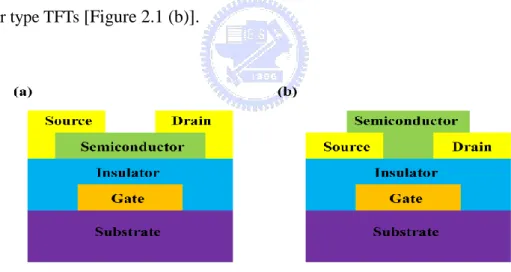
2.1 Structures of Thin Film Transistors
According to the different position of source and drain, OTFTs can be classified to two common device structures: top-contact which also is called the inverted
staggered type [Figure 2.1 (a)].and bottom-contact which is also called the inverted
coplanar type TFTs [Figure 2.1 (b)].
2.2 The Operation of Thin Film Transistors
The TFTs can be divided into two parts: n-type and p-type channel, according to the type of transported charges in the semiconductor. The majority carriers are electrons in the n-type channel. On the other hand, the majority carriers are holes in p-type channel. The TFTs can also be classified into two parts: the depletion-mode and the enhancement-mode, based on whether drain current flows through TFTs when no voltage is applied to gate electrode. For the enhancement-mode TFTs, only leakage current flows through the TFTs without applying the gate voltage and the device is off. For the depletion-mode TFTs, the drain current flows through the TFTs without applying the gate voltage and the device is on. If trying to turn off the depletion-mode TFTs with n-type channel, the gate electrode will be biased negatively with respect to the grounded source electrode.
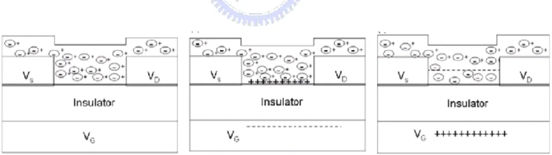
The energy band diagrams and the schematics of TFTs operation in an n-type accumulation mode as shown in Figs. 2-2 and 2-3 are introduced to explain the three operation modes of TFTs. When no gate voltage is applied, the semiconductor is in an equilibrium state. After a negative bias is applied on the gate electrode, the delocalized electrons in the channel are repelled from the semiconductor/gate insulator interface. The effect creates a depletion region of positive charge, as indicated by the positive curvature in the conduction band and the valance band near the insulator as shown in Fig. 2-2 (b). This result conducts the depletion region of carriers as shown in Fig. 2-3 (b). The higher bias on the gate electrode, the larger depletion the region expands. Finally, all of the semiconductor layer will be depleted. When a positive gate bias is applied, delocalized electrons in the channel are attracted to the semiconductor/gate insulator interface, and creating electron accumulation at the interface. The outcome can be indicated by the negative curvature in the
conduction band and valance band near the insulator as shown in Fig. 2-2 (c). Then, the accumulation region is formed as shown in Fig. 2-3 (c). These accumulated electrons at the semiconductor/insulator interface provide a current conduction path and form the channel.
Figure 2.2 The semiconductor energy band diagram when (a) unbiased, (b) negative gate voltage bias, and (c) positive gate voltage bias, respectively.
Figure 2-3 Schematic of TFTs operation in accumulation mode: (a) unbiased, (b) negative gate voltage bias, and (c) positive gate voltage bias, respectively.
The quantities of charges accumulated in the active layer are proportional to the gate bias and the capacitance of the insulator. In fact, the deep traps have to be filled firstly at interfacial states, and then induce extra mobile charges. In other words, the VGS have to be biased higher than the threshold voltage (VTh). So VGS-VTh is the
effective driving voltage to accumulate more mobile charge carriers. The interfacial potential can be created an internal voltage at the semiconductor interface upon the insulator at zero gate bias and thus cause accumulation of additional charges (mobile or immobile) in the channel so that a obvious turn-on voltage shift is exhibited in the transfer characteristics [32,33] .
Figure 2.4 Carrier concentration diagram of TFT and associated current-voltage characteristics.
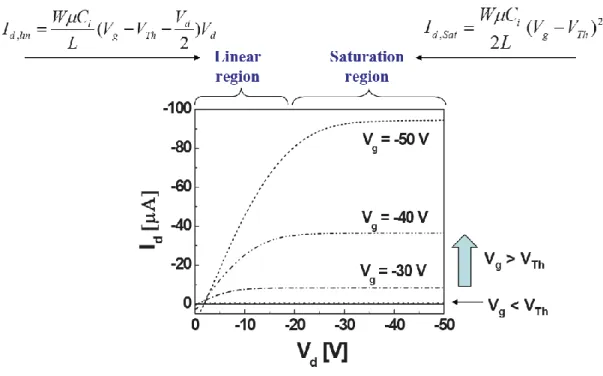
Figure 2.5 illustrates the basic operating modes and associated current-voltage characteristics. When drain-to-source voltage is zero, the charge carrier concentration in the transistor channel is uniform. Therefore, a linear slope of charge density can be observed when a small source-drain voltage is applied. In the linear regime, the quantities of charges flowed in the active layer are proportional to the gate bias. From the source [V(X=0) = 0 V] to the drain electrode [V(X=L) = VDS], the potential V(x)
within the channel increases linearly. When VDS = VGS - VTH, the channel becomes
pinched- off. A depletion region is formed near the drain electrode because the voltage difference between the local potential V(x) and the gate voltage is lower than the threshold voltage. Now only a space-charge-limited saturation current can flow across this region. Applying a higher drain-to-source voltage, it pushed the pinch point slightly toward the source. Eventually, in common situations, the channel length is much longer than the width of this depletion part, and the higher drain voltage would not lead to an additional drain current.
2.3 The Parameters Extraction of TFTs
There are two electrical characteristics curves. The one plot is ID - VD transfer
characteristics as shown in Figure 2.6. The ID versus VD relation is measured under
the constant VG and sweeping VD. There are two modes which are the linear and
saturation modes in the ID - VD curves. The TFT is operated in the linear mode when
voltage, subthreshold swing, and on-off ratio. Although the transportation mechanism is different between the organic materials and inorganic materials, the transfer characteristics are similar. Now we introduce a formula as the following section:
First, from Ohm’s law, we know
(2-1)
, where σ is the conductivity, W is the channel width, L is the channel length , and t is the thickness of charged layer in the channel.
Figure 2.6 The ID-VG transfer characteristics of a p-typeTFT.
The equation 2-1can be rewritten as:
μ
(2-2)
, where nind is the number density of induced charges in the channel and μ is the
carrier mobility.
We assume the average value of induced charges is
(2-3)
Then we can substitute equation 2-3 into equation 2-2, and obtain:
When VD > VG - VTh, the TFT is operated in a saturation regime and the equation 2-4
will be become:
(2-5)
, where μsat is the carrier mobility in the saturated region, and the μsat is usually
higher.
The mobility μ can be calculated by differentiating the square root of ID in
saturation mode as:
μ
(2-6)
In the figure 2.7, the slop and threshold voltage can be measured from the ID0.5 –
VG curves.
The subthreshold swing (S.S.) is a parameter to determine the switch speed of a transistor. It can be calculated by the following equation 2-7.
(2-7)
The dimension of subthreshold swing is V/decade. The subthreshold swing gives the degree of the switch property of a transistor.
Chapter 3
Experimental and Analysis Methods
3.1
Preface
The top-contact structure was chosen to fabricate the TFTs in this study The structure of the top-contact TFT is shown in Figure 2.1a.
3.1.1 Preparation of Substrates
We use heavily doped n-type silicon wafers with thermal SiO2 to fabricate the
devices. The top SiO2 layer was 200 nm thick, and the sheet resistance was about
0.001~0.003 ohm-cm. The capacitance per unit area in the SiO2 layer was 14.2
nF/cm2. The conductance of the wafers is high enough to serve as the gate electrode.
Step 2: Put the substrates into a Teflon container and soak the substrates in DI water
into an ultrasonic cleaner for 20 minutes. Then rinse the substrates by DI water for 5 minutes.
Step 3: Put the substrates into a Teflon container and soak the substrates in ACE into
an ultrasonic cleaner for 20 minutes. Organic pollutants would be swept away in this step. Then rinse it again by DI water in 5 minutes.
Step 4: Put the substrates into a Teflon container and soak the substrates in IPA into
an ultrasonic cleaner for 20 minutes. The residual acetone and water molecules would be taken away by IPA. Then rinse it repeatedly by DI water in 5 minutes.
Step 5 : Dry the substrates by nitrogen shower, and then these substrates were placed
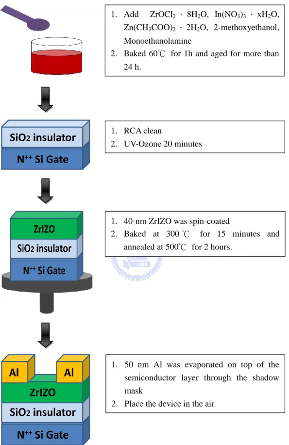
3.2 The Material
Zirconium indium zinc oxide (ZrIZO) [Figure 3.1(a)] was used as the active layer of the TFTs. It was fabricated from zirconium dichloride oxide octahydrate [ZrOCl2.8H2O] [Figure 3.1(b)], indium nitrate pentahydrate [In(NO3)3.xH2O]
[Figure 3.1(c)], and zinc acetate dehydrate [Zn(CH3COO)2.2H2O] [Figure 3.1(d)]
in 2-methoxyethanol [Figure 3.1(e)]. Monoethanolamine [Figure 3.1(f)] was also added because adding Monoethanolamine in the same concentration with zinc acetate dehydrate could make the solution more stable.
Figure 3.1 The structure of materials used in this experiment. [(a) was adapted from Jin-Seong Park Lab [36]]
[(b) was adapted from http://www.jhyb.com.cn/goods-1680.html] [(c) was adapted from
http://www.chemicalbook.com/ChemicalProductProperty_CN_CB2619716.htm] [(d) was adapted from http://dailymed.nlm.nih.gov/dailymed/drugInfo.cfm?id=1081] [(e) was adapted from http://en.wikipedia.org/wiki/File:2-Methoxyethanol.png] [(f) was adapted from
3.3 Device Fabrication Processes
3.3.1 Spin-Coating of the ZrIZO as the Active Layer
The total concentration of the metal precursors was 0.25M. Before spin-coating of the film, the ZrIZO solution was heated at 60℃ for 1 hour and then aged for more than 24 hours.
The substrates were subject to UV-Ozone treatment for 20 minutes. The ozone molecules would burn the organic contaminant on substrates, and the particles were taken away by an air flow.
The spin rate was set to 1500 r.p.m for 1 minute. The cleaned SiO2 substrates
were covered with an active layer of 40 nm thick, which was prepared by spin coating of the solution of ZrIZO. After spinning, the ZrIZO films were soft baked at 300℃ for 15 minutes.
3.3.2 Evaporation of Metal Electrodes
Before the deposition of source and drain electrodes, the device was pre-annealed in air at 500℃ for 2 hours. Finally, aluminum 50nm was deposited as the source and drain electrodes by thermal evaporation under a pressure less than 5×10⁻⁶ torr through a shadow mask. The channel was 200 μm wide and 120 μm long.
Figure 3.2 The flow chart of the device fabrication process.
1. Add ZrOCl2. 8H2O, In(NO3)3. xH2O,
Zn(CH3COO)2. 2H2O, 2-methoxyethanol,
Monoethanolamine
2. Baked 60℃ for 1h and aged for more than 24 h.
1. RCA clean
2. UV-Ozone 20 minutes
1. 40-nm ZrIZO was spin-coated
2. Baked at 300 ℃ for 15 minutes and annealed at 500℃ for 2 hours.
1. 50 nm Al was evaporated on top of the semiconductor layer through the shadow mask
3.4 Measurements and Analysis of TFTs
3.4.1 Electrical Characteristics
We measured the electrical properties of the devices by Keithley 4200 IV measurement system at room temperature. For ZrIZO devices, we applied a positive gate voltage to accumulate electrons in the channel near the semiconductor/insulator interface. In the ID-VD measurement, we swept the gate bias from 0 to 60Volts, and
the gate voltage step was 15 V from VG = 0 V to VG = 60 V. Besides, in the ID-VG
measurement, the drain bias swept from 10 to 30V, and the drain voltage step was 10 V from VG = 10 V to VG = 30 V.
3.4.2 Measurement of Surface Morphology
In this study, we used the atomic force microscope (AFM) to measure the surface morphology of the materials. By the interaction of the van der Waals force between the tip of the cantilever and the surface topology of the sample, the cantilever vibrates at different frequencies depending on the magnitude of the interaction. Detecting a laser beam reflected by the cantilever can sense the tiny vibration of the cantilever, the computer record these detected signals and re-construct the surface morphology of samples. The interaction force between the two atoms where one is on the tip of the cantilever and the other is on the surface of sample depends on their distance as show in Figure 3.3. Similarly, Figure3.4 illustrates the configuration of AFM. From the surface morphology, we can find the relationship between the transfer characteristic and the graining formation of the organic semiconductor.
3.4.3 X-ray Photoelectron Spectroscopy Measurement
X-ray photoelectron spectroscopy (XPS) is a widely used technique that can measure the elemental composition, the chemical state and the electron state of the elements that exist in materials. It suits to study core-level electron spectroscopy because of its high energy and short wavelength. Figure 3.5 shows the configuration of XPS. The energy (hν) of the x-ray was incident into the sample, and the core-level electron of an atom possesses exceed energy is excited. The electron possesses the kinetic energy Ek. Ek and hν are related by the following equation: Ek = hν- Eb – φ, φ
is the energy of the material work function and Eb is the binding energy of an atom.
This kind of electron is called photoelectron. In other words, by measuring the energy of the photoelectrons, we can plot photoelectron intensity versus the electron energy. From the chart, we can get the information of the material.
Figure 3.5 The operation of x-ray photoelectron spectroscopy.
3.4.4 X-ray Diffraction Measurement
High-resolution x-ray diffraction is used to characterize the thickness, and the crystallographic structure in thin epitaxial films. When x-ray is incident on the material of a regular structure, the crystalline solids reflect x-ray and produce Bragg’s diffraction. The interference is constructive when the phase shift is a multiple of 2π. The relation can be indicated by the following formula: nλ=2dsinθ, where n is an integer, λ is the wavelength of incident wave, d is the spacing between the planes in the atomic lattice, and θ is the angle between the incident ray and the scattering planes. These crystals, at certain specific wavelengths and incident angles, produce intense peaks of reflected radiation. In other words, we can use this information, including incident angle, peak position and intensity to construct the crystal structure.
3.4.5 UV/Visible Spectroscopy Measurement
The UV/Visible absorption of films was measured on Perkin Elmer Lambda 650. The light sources of the UV/Visible spectroscopy are provided by D2 and W. The UV
wave band is provided by D2, and the visible light wave band by W. The absorption,
A, is defined as A=log (I0/I), where I0 is the intensity of the incident light and I is the
Chapter 4
Results and Discussion
4.1 The Effect of the Zr content
The mole ratio of Zr was varied from 0 to 1 while the In: Zn mole ratio was fixed at 5:5. (i.e., the mole ratio of ZIZO were Zr: In: Zn =0: 5: 5, 0.1: 5: 5, 0.2: 5: 5, 0.5: 5: 5, and 1: 5: 5) The variation in transfer and output characteristics of the solution-processed ZIZO TFTs with the Zr molar ratio after 8th day was described in Figure 4.1 and Table 4.1. The device exhibited typical n-channel behavior operation in the enhancement mode. As the Zr content increased, both on and off current decreased. This phenomenon was attributed to the fact that Zr acted as a carrier suppressor, like Ga and Hf. In fact, the numbers of electron carriers were reduced due to the decreased number of oxygen vacancies. We considered that this suppressing ability should be attributed to its high electron negativity (EN = 1.4). This suppressing ability is stronger than that of Ga, whose EN is equal to 1.7. And a large on-off current ratio was observed (>107). Because subthreshold swing (SS) is related to the bulk and interfacial trap states (Nt) in the TFTs, the total interfacial trap state
-40 -20 0 20 40 10-12 10-11 10-10 10-9 10-8 10-7 10-6 10-5 10-4 10-3 10-2
D
ra
in
C
u
rr
e
n
t
(A
)
Gate Voltage (V)
ZIZO 0:5:5 ZIZO 0.1:5:5 ZIZO 0.2:5:5 ZIZO 0.5:5:5 ZIZO 1:5:5Figure 4.1 The ID-VG transfer characteristics of the ZIZO TFTs at VD = 60 V
prepared with various Zr compositions (L = 120μm and W = 200μm).
Table 4.1 Comparison of the electrical characteristics for the solution-processed ZIZO TFTs with various Zr ratio.
Zr:In:Zn mole ratio μ (cm 2 /Vs) I on-off VTh (V) SS (V/dec) Nt (cm -2 ) 0:5:5 4.55 1.63×10³ -1.13 8.11 1.28×10¹³ 0.1:5:5 3.80 1.22×10⁷ 0.44 0.42 5.72×10¹¹ 0.2:5:5 2.98 1.48×10⁷ 2.35 0.967 1.44×10¹² 0.5:5:5 1.04 9.25×10⁶ 9.39 1.146 1.72×10¹² 1:5:5 0.263 5.3×10⁶ -18.34 1.277 2.01×10¹³
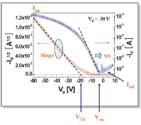
From Table 4.1, the optimized condition of the ZIZO TFTs was Zr: In: Zn=0.1: 5: 5. As shown in Figure 4.2, the device exhibited a high saturation current which was higher than 10-3A. The saturation field-effect mobility (μFE) and the on-off current
ratio were estimated to be 3.8cm2/Vs and ~107, respectively. The threshold voltage (VTh) was 0.44 V. The subthreshold swing is 0.42 V/dec. Overall, the characteristics
of the solution-processed ZIZO TFT are almost comparable with those of the device made by sputtering methods.
0 10 20 30 40 0.0 5.0x10⁻⁴ 1.0x10⁻³ 1.5x10⁻³ 2.0x10⁻³ D ra in C u rr e n t (A ) Drain Voltage (V) VG=15V VG=30V VG=45V VG=60V 10-12 10-11 10-10 10-9 10-8 10-7 10-6 10-5 10-4 10-3 10-2 D ra in C u rr e n t (A ) VD=10V VD=20V VD=30V
4.2 The Effect of Pre-annealing Temperature
The pre-annealing temperature was varied from 300℃ to 500℃. The variation in the transfer and output characteristics of the solution-processed ZIZO TFTs fabricated with various pre-annealing temperature is described in Figure 4.3 and Table 4.2. The device exhibited typical n-channel behavior in the enhancement mode. When the pre-annealing temperature increased, the electrical characteristics were obviously improved. When the pre-annealing temperature was higher than 400℃, the device should apparent field effect. On the contrary, when the pre-annealing temperature was below 400℃, the device only exhibited a very low current presumably due to the low crystallinity of the ZIZO thin film.
Figure 4.3 The transfer characteristics of the ZIZO TFT at VD = 60 V prepared
with various pre-annealing temperature (L = 120μm and W = 200μm).
Table 4.2 Comparison of the electrical characteristics for the solution-processed ZIZO TFTs fabricated with various pre-annealing temperature.
Pre-annealing Temperature μ (cm2/Vs) I on-off VTh (V)
300℃ … … …
400℃ 0.59 3.03×10⁶ -6.78
4.3 The Effect of the Adding NaOH
When the processes of solution-processed ZIZO TFT were finished, we observed from the transfer curve that the device had a high off current. We preserved the device in ambient environment in which the relativity humidity was about 60%. Figure 4.4 shows the electrical transfer performance of the device measured from the 1st day to the 15th day. We could observe that the off current remarkably decreased gradually. Similarly, we could see that the transfer performance became stable after the 8th day. We inferred that the chemical reaction had not been finished after the device was completed.
-40 -20 0 20 40 10-12 10-11 1x10⁻¹⁰ 1x10⁻⁹ 1x10⁻⁸ 1x10⁻⁷ 1x10⁻⁶ 1x10⁻⁵ 1x10⁻⁴ 1x10⁻³ 1x10⁻²
Drain Curre
nt (A
)
Gate Voltage (V)
1st day 3rd day 5th day 7th day 8th day 9th day 10th day 12th day 14th day 15th dayFigure 4.4 The ID-VG transfer characteristics of ZIZO TFT with the ratio of Zr: In:
There were probably three stages during the formation of ZIZO semiconductor. According to order, the first stage was decomposition and hydrolysis. The second stage was dehydroxylation and alloying. The last stage was crystallization. In the second stage, after adding hydroxyl in the solution, such as NaOH, it could speed up the dehydroxylation reaction. Figure 4.5 and Table 4.3 showed the transfer characteristics and the parameters. After the addition of 0.03M NaOH, the electrical characteristics became stable in 9 days, suggesting that adding NaOH could accelerate the reaction effectively.
-40
-20
0
20
40
10
-1210
-111x10
-101x10
-91x10
-81x10
-71x10
-61x10
-51x10
-41x10
-31x10
-2D
ra
in
C
u
rr
e
n
t
(A
)
Gate Voltage (V)
ZIZO 0:5:5 (no NaOH) ZIZO 0.1:5:5 (no NaOH) ZIZO 0.2:5:5 (no NaOH) ZIZO 0.5:5:5 (no NaOH) ZIZO 0:5:5 (add NaOH) ZIZO 0.1:5:5 (add NaOH) ZIZO 0.2:5:5 (add NaOH) ZIZO 0.5:5:5 (add NaOH)
Figure 4.5 The ID-VG transfer characteristics of ZIZO TFT at VD = 60 V with
Table 4.3 Comparison of the electrical characteristics for solution-processed ZIZO TFT with different ratio with/without adding 0.03M NaOH.
μ (cm2/Vs) I On-off VTh (V) Reaction day
0:5:5 (no NaOH) 4.55 1.63×10³ -1.13 10th 0.1:5:5 (no NaOH) 3.80 1.22×10⁷ 0.44 10th 0.2:5:5 (no NaOH) 2.98 1.48×10⁷ 2.35 10th 0.5:5:5 (no NaOH) 1.04 9.25×10⁶ 9.39 10th 0:5:5 (add NaOH) 3.18 1.88×10³ -6.87 1st 0.1:5:5 (add NaOH) 3.39 5.72×10⁶ -5.69 1st 0.2:5:5 (add NaOH) 2.93 1.53×10⁷ -10.99 1st 0.5:5:5 (add NaOH) 1.17 7.66×10⁶ 4.75 1st
4.4 The Bias Stress Measurement
The electrical output performance under the different bias stress was displayed in Figure 4.6. When a gate bias of 10 V was applied, we can see that the △VTh
became stable after 1×10⁴ seconds. On the contrary, if a bias stress of 20V was applied, the threshold voltage shift continued to increase with time.
Figure 4.6 The variation of VTh for the ZIZO TFTs as a function of stress
4.5 The Morphological Analysis of the Active Films
The height-mode and phase-mode images of the ZIZO films prepared with different Zr ratios were displayed in Figure 4.7. Figure 4.7(a), (c) and (e) showed the height mode images of the thin film prepared with the ratio of Zr: In: Zn = 0: 5: 5, Zr: In: Zn = 0.1: 5: 5 and Zr: In: Zn = 0.5: 5: 5, respectively, on the SiO2 films. Similarly,
Figure 4.7 (b), (d) and (f) showed the phase mode images of the thin films prepared with the ratio of Zr: In: Zn = 0: 5: 5, Zr: In: Zn = 0.1: 5: 5 and Zr: In: Zn = 0.5: 5: 5 deposited on the SiO2 films. In the height-mode images, the films deposited with
different ratios exhibit a smooth surface morphology. The surface roughnesses of the films prepared with the ratio of Zr: In: Zn = 0: 5: 5, Zr: In: Zn = 0.1: 5: 5 and Zr: In: Zn = 0.5: 5: 5 were 0.375nm, 0.396 nm and 0.325 nm, respectively. When the Zr content was increased in the film, the roughness still did not change significantly. However, in the phase mode images, we could observe many small grains on the surface. When the Zr content was increased, number of the grains was decreased gradually.
Figure 4.8 shows the height mode and phase mode images for the device annealed with different pre-annealing temperatures. When the pre-annealing temperature was increased, the roughness also increased. The roughness of the thin film prepared at 300℃, 400℃ and 500℃ was 0.233nm, 0.359nm and 0.396nm, respectively. When the pre-annealing temperature was increased, the grain size became larger, thereby improving the charge transport. Therefore, the device exhibited higher mobility.
Figure 4.8 The height-mode and phase-mode images for the thin film prepared with the ratio of Zr: In : Zn = 0.1: 5 : 5 at various pre-annealing temperatures measured by AFM: (a) pre-annealing temperature: 300 ℃ (b) pre-annealing temperature: 300 ℃ (c) pre-annealing temperature: 400 ℃ (d) pre-annealing temperature: 400 ℃ (e) pre-annealing temperature: 500 ℃ (f) pre-annealing temperature: 500℃. (a)(c)(e) are height-mode images. (b)(d)(f) are phase mode images.
4.6 The Analysis of XRD Measurement
Figure 4.9 shows the x-ray diffraction (XRD) pattern of the ZIZO films deposited on SiO2 surfaces. We could analysis the crystallization of the ZIZO thin
films from the figure. Unfortunately, we found that no matter which conditions we used, the XRD patterns were all similar: all ZIZO films exhibited amorphous phase, suggesting that the addition of Zr atoms effectively inhibited the crystallization of InZnO.
20
30
40
50
60
70
Intensity (a.
u.)
2 Theda Degree
ZIZO 0:5:5
ZIZO 0.1:5:5
ZIZO 0.2:5:5
ZIZO 0.5:5:5
4.7 The Analysis of UV/Vis Spectroscopy Measurement
Figure 4.10 shows the transmittances of the ZIZO thin films deposited on the ITO glasses as a function of Zr content. The average transmittance of the ZIZO thin films was higher than 98% in the visible range. We also found that as the Zr content was increased, optical transmittance of the film was increased. The addition of Zr atoms probably increases of the band gap..300 400 500 600 700 800 900
90
92
94
96
98
100
ZIZO 0:5:5
ZIZO 0.1:5:5
ZIZO 0.5:5:5
Tra
nsm
ittan
ce (%
)
Wavelength (nm)
Plots of (ahv)2 versus absorption energy for the ZZTO thin films were shown in Figure 4.11. The optical absorption coefficient (a) and the optical energy band gap are related by the following equation:
where h is Planck’s constant, v is the frequency of the incident photon, C is a constant for a direct transition, and a is the optical absorption coefficient. As the ratio of Zr content increased, the optical band gap increased, from3.64 to 3.68 eV. Wide optical band gaps of thin films have large activation energies between the Fermi level (Ef)
and the conduction band minimum (Ec), and thermally activated carriers were
reduced according to n= Nc exp[-(Ec-Ef)/kT]. The resistivity of the ZIZO thin films
4.8 The Analysis of XPS Measurement
XPS spectra of Zr, In, Zn ions with respect to the Zr content, and pre-annealing temperature was shown in the Figure 4.11. The Zr 3d5/2, In 3d5/2, Zn 2p3/2, centered at
183.4, 445.6, and 1022.8 eV, which indicated Zr-O, In-O, and Zn-O bonds, respectively.
First, we investigated the effect of the Zr content. As expected the intensity of the Zr 3d5/2 peak decreased the decreasing Zr content. The peak of Zr 3d5/2 centered at
183.4 eV was attributed to the fully oxidized zirconium. When the Zr content was decreased, it could cause a shift in the lower binding energy of In 3d5/2 and Zn 2p3/2
peaks from 445.6 and 1022.8 eV to 445.2 and 1022.2 eV, respectively.
Finally, we investigated the effect of the exposure to the atmosphere. In Figure 4.12, we observed that the binding energy of the peaks for the device prepared with the ratio of Zr: In: Zn = 0.5: 5: 5 was different than others after 2 days. According to Figure 4.4, we observed that the transfer performances became stable after 8 day. We inferred that the chemical reaction had not been completed yet. Therefore, the XPS pattern was similar to that of the device. On the other hand, after 7th day, the Zr 3d5/2,
In 3d5/2 and Zn 2p3/2 peaks shifted from 181.8, 444.2 and 1021.2 eV to 183.4, 445.6
and 1022.8 eV respectively. The shifted peaks indicated that a chemical reaction occured.
According the pattern of XPS, we calculated the real ratio of Zr: In: Zn = 0: 5: 5, 0.1: 5: 5, 0.5: 5: 5was 0: 3: 2, 1: 2: 2, 4: 11: 5, respectively.
Figure 4.13 shows the O 1s region of the XPS spectra with respect to Zr content. The O 1s peak could be deconvoluted into two peaks centered at 531.3 and 532.9 eV, determined by Gaussian fitting. The O 1s peak could be explained with the binding state of oxygen with metals. The lower energy oxygen peaks was defined as OI, the
higher as OII. OI represented the O2- ions combined with Zr, In and Zn ions in the
ZIZO system. OII was associated with oxygen vacancies in the ZIZO compound. Ototal
denoted the total O 1s peak area. When increasing the Zr content, the OII/Ototal value
representing the ratio of oxygen vacancies gradually decreased from 0.486 to 0.289. Not only OII/Ototal but also OII/OI was decreased from 0.967 to 0.6310. Therefore,
incorporating Zr reduced oxygen vacancies, indicating that Zr acted as a carrier suppressor effectively.
Table 4.4 Variation in the area ratio of O 1s Zr:In:Zn Binding Energy (eV) Ratio Area OII/OI 0:5:5 531.3 OI/Ototal 0.502 0.967 532.9 OII/Ototal 0.486 0.1:5:5 531.3 OI/Ototal 0.516 0.6337 532.9 OII/Ototal 0.327 0.5:5:5 531.3 OI/Ototal 0.458 0.6310 532.9 OII/Ototal 0.289
Chapter 5
Conclusion
In conclusion, we have demonstrated a solution-processable approach for manufacturing high-performance ZrInZnO (ZIZO) thin film transistors (TFTs). We studied Zr as a candidate material for carrier suppressor in the IZO systems in place of other common suppressors, such as Ga. The ZIZO TFTs exhibited a field effect mobility of 3.8 cm2/Vs, an on-off ratio of ~107. The threshold voltage (Vth) was 0.44
V and the subthreshold swing was 0.42 V/dec. The threshold voltage became stable under the bias stress. Further, ZIZO thin film was amorphous. When the pre-annealing temperature increased, the crystallization was improved. Analysis of the O 1s peak in the XPS spectra showed decreasing the O2- ions related to the variation in the concentration of oxygen vacancies which can supply free electrons. By adding NaOH, we could speed up the hydroxylation reaction. Overall the device performance is almost comparable with that of the device made by conventional cosputtering methods. Our method offers another possible way to low-cost, high-through manufacture for next generation TFTs for display applications.
Reference
[1] J.-H. Lee, D.-H. Kim, D.-J. Yang, S.-Y. Hong, K.-S. Yoon, P.-S.Hong,C.-O. Jeong, H.-S. Park, S. Y. Kim, S. K. Lim, and S. S. Kim, “World’s Largest (15-inch) XGA AMLCD Panel Using IGZO Oxide TFT,” SID Symposium Digest Tech Papers, 625, 2008.
[2] J. K. Jeong, J. H. Jeong, J. H. Choi, J. S. Im, S. H. Kim, H. W. Yang, K.N. Kang, K. S. Kim, T. K. Ahn, H.-J. Chung, M. Kim, B. S. Gu, J.-S. Park,Y.-G. Mo, H. D. Kim, and H. K. Chung, “12.1-inch WXGA AMOLED Display Driven by Indium-Gallium Zinc Oxide TFTs Array,” SID Symposium Digest Tech Papers, 1, (2008).
[3] H. Hosono, “Ionic amorphous oxide semiconductors: Material design, carrier transport, and device application,” J. Non-Crystalline Solids 352, 851 (2006)
[4] H. Hosono, “Working hypothesis to explore novel wide band gap electrically
conducting amorphous oxides and examples,” J. Non-Crystalline Solids, 198–200,
165–169 (1996).
[5] J. F. Wager, “Applied Physics Transparent Electronics,” Science, 300, 1245 (2003). [6] P. F. Carcia, R. S. Mclean, M. H. Reilly, and G. Lunes, “Transparent ZnO thin-film transistor fabricated by rf magnetron sputtering,” Jr. Appl. Phys. Lett., 82, 1117 (2003).
[7] K. L. Chopra, S. Major, and K. Pandya, “Highly transparent and conducting
indium-doped zinc oxide films by spray pyrolysis,” Thin Solid Films, 102,1 (1983).
[8] Y. Ohya, T. Niwa, T. Ban, and Y. Takahashi, “Thin Film Transistor of ZnO Fabricated by Chemical Solution Deposition,” Jpn. J. Appl. Phys., 40, 297 (2001).
[9] K. Nomura, A. Takagi, T. Kamiya, H. Ohta, M. Hirano, and H.Hosono, “Amorphous Oxide Semiconductors for High-Performance Flexible Thin-Film Transistors,” Jpn. J. Appl. Phys., 45, 4303-4308 (2006).
[10] H. Yabuta, M. Sano, K. Abe, T. Aiba, T. Den, H. Kumomi, K.Nomura, T. Kamiya, and H. Hosono, “High-mobility thin-film transistor with amorphous InGaZnO4 channel fabricated by room temperature rf-magnetron sputtering,” Appl. Phys. Lett., 89, 112123 (2006).
[11] N. F. Mott, “Silicon dioxide and the chalcogenide semiconductors; similarities
and differences,” Adv.Phys., 26, 363–391 (1977).
[12] K. Nomura, H. Ohta, A. Takagi, T. Kamiya, M. Hirano, and H. Hosono, “Room-temperature fabrication of transparent flexible thin film transistors using amorphous oxide semiconductors,” Nature, 432, 488 (2004).
[13] P. Barquinha, A. Pimentel, A. Marques, L. Pereira, R. Martins and E. Fortunato, “Influence of the semiconductor thickness on the electrical properties of transparent TFTs based on indium zinc oxide,” J. Non-Cryst. Solids, 352, 1749 (2006).
[14] P. Gorrn, P. Holzer, T. Riedl, W. Kowalsky, J. Wang, T. Weimann, P. Hinze and S. Kipp, “Stable of transparent zinc tin oxide transistors under bias stress, ”Appl. Phys. Lett.,
90, 063502 (2007).
[15] J.S. Park, K. S. Kim, Y. G. Park, Y. G. Mo, H. D. Kim, and J. K. Jeong, “Novel ZrInZnO Thin-film Transistor with Excellent Stability,” Adv. Mater 21, 329-333 (2009).
[16] E. Fortunato, P. Barquinha, A. Pimentel, A. Goncalves, A. Marques, L.
[18] R. L. Hoffman, B. H. Norrs, J. F. Wager, “ZnO-based transparent thin film transistors, “Room temperature deposited indium zinc oxide thin film transistors,” Appl. Phys. Lett. 82, 733 (2003).
[19] Y.-L. Wang, F. Ren, W. Lim, D. P. Norton, S. J. Pearton, I. I. Kravchenko, J. M. Zavada, “Room temperature deposited indium zinc oxide thin film transistors,” Appl. Phys. Lett. 90, 232103 (2007).
[20] B. Yaglioglu, H. Y. Yeom, R. Beresford, D. C. Paine, “Magnetotransport properties of Ge channels with extremely high compressive strain,” Appl. Phys. Lett.
89, 062103 (2006).
[21] C. G. Choi, S.-J. Seo, B.-S. Bae, Electrochem. “Solution-processed indium zinc oxide transparent thin-film transistors,” Solid-State Lett 11, H7 (2008).
[22] H. Yabuta, M. Sano, K. Abe, T. Aiba, T. Den, H. Kumomi, K. Nomura, T. Kamiya, H. Hosono, “Control of p- and n-type conductivities in Li-doped ZnO thin films,” Appl. Phys. Lett. 89, 112123 (2006).
[23] M. Kim, J. H. Jeong, H. J. Lee, T. K. Ahn, H. S. Shin, J. S. Park, J. K. Jeong, Y. G. Mo, H. D. Kim, “High mobility bottom gate InGaZnO thin film transistors with SiOx etch stopper,” Appl. Phys. Lett. 90, 212114 (2007).
[24] J. S. Park, J. K. Jeong, Y. G. Mo, H. D. Kim, “Improvements in the device characteristics of amorphous indium gallium zinc oxide thin-film transistors by Ar plasma treatment,” Appl. Phys. Lett. 90, 262106 (2007).
[25] J. K. Jeong, J. H. Jeong, H. W. Yang, J.-S. Park, Y.-G. Mo, H. D. Kim, “High performance thin film transistors with cosputtered amorphous indium gallium zinc oxide channel,” Appl. Phys. Lett. 91, 113505 (2007).
[26] J. H. Jeong, H. W. Yang, J.-S. Park, J. K. Jeong, Y.-G. Mo, H. D. Kim, J. Song, C. S. Hwang, “Origin of subthreshold swing improved in amorphous indium gallium zinc oxide transistor,” Electrochem. Solid-State Lett. 11, H157 (2008).
[27] K. Nomura, H. Ohta, A. Takagi, T. Kamiya, M. Hirano, H. Hosono, “Room-temperature fabrication of transparent flexible thin-film transistors using amorphous oxide semiconductors,” Nature 432, 488 (2004).
[28] G. H. Kim, W. H. Jeong, B. D. Ahn, H. S. Shin, H. J. Kim, H. J. Kim. M. -K. Ryu, K. –B. Park, J. –B. Seon, and S. –Y. Lee, “Investigation of the effects of Mg incorporation into InZnO for high-performance and high-stability solution-processed thin film transistors,” Appl. Phy. Lett 96,163506 (2010).
[29] W. H. Jeong, G. H. Kim, H. S. Shin, B. D. Ahn, H. J. Kim, M, -K. Rye, K. -B. Park, J. -B. Seon, and S. -Y. Lee, “Investigating addition effect of hafnium in InZnO thin film transistors using a solution process,” Appl. Phy. Lett. 96, 093503 (2010). [30] Y. Choi, G. Kim, W. Jeong, J. Bae, H. Kim, J. Hong, J. Yu, “Carrier-suppressing effect of scandium in InZnO systems for solution-processed thin film transistor,” Appl. Phys Lett. 97, 162102 (2010).
[31] D. N. Kim, D. L. Kim, G. H. Kim, S. J. Kim, Y. S. Rim, W. H. Jeong, and H. J. Kim, “The effect of La in InZnO systems for solution-processed amorphous oxide thin-film transistors,” Appl. Phys Lett. 97, 192105 (2010).
[32] S. Kobayashi, T. Nishikawa, T. Takenobu, S. Mori, T. Shimoda, T. Mitani, H. Shimotani, N. Yoshimoto, S. Ogawa, and Y. Iwasa, “Control of carrier density by self-assembled monolayers in organic field-effect transistors,” Nat. Mater. 3, 317 (2004).
[33] K. P. Pernstich, S. Haas, D. Oberhoff, C. Goldmann, D. J. Gundlach, B. Batlogg, A. N. Rashid, and G. Schitter, “Threshold voltage shift in organic field effect transistors by dipole monolayers on the gate insulator,” J. Appl. Phys. 96, 6431
[35] G. Horowitz, F. Dellofre, F Garnier, R. Hajlaoui, M. Hmyene, and A. Yassar, Synth, “All-organic field-effect transistors made of π-conjugated oligomers and polymeric insulators,” Met. 54, 435 (1993).
[36] Jin-Seong Park, KwangSuk Kim, Yong-Gil Park, Yeon-Gon Mo, Hye Dong Kim, and Jae Kyeong Jeong, “Novel ZrInZnO Thin-film Transistor with Excellent Stability,” Adv. Mater. 2009, 21, 329–333
![Figure 1.1 Schematic of an active matrix display layout. [Adapted from http://www.wtec.org/loyola/dsply_jp/c5_s2.htm]](https://thumb-ap.123doks.com/thumbv2/9libinfo/8122897.165962/12.892.159.748.575.1007/figure-schematic-active-matrix-display-layout-adapted-loyola.webp)

![Figure 3.1 The structure of materials used in this experiment. [(a) was adapted from Jin-Seong Park Lab [36] ]](https://thumb-ap.123doks.com/thumbv2/9libinfo/8122897.165962/30.892.150.749.109.486/figure-structure-materials-used-experiment-adapted-seong-park.webp)