使用完全矽化閘極-高介電常數介電質之低臨界電壓金氧半電晶體
67
0
0
全文
(2) 使用完全矽化閘極-高介電常數介電質之低臨界電壓金氧半電晶體 A Low Threshold Voltage n-MOSFET Using Fully Silicided Gate and High-κ Dielectric. 研 究 生:陳冠霖. Student:Guan-Lin Chen. 指導教授:荊鳳德. Advisor:Dr. Albert Chin. 國 立 交 通 大 學 電子工程系 電子研究所碩士班 碩 士 論 文. A Thesis Submitted to Department of Electronics Engineering & Institute of Electronics College of Electrical and Computer Engineering National Chiao Tung University in Partial Fulfillment of the Requirements for the Degree of Master In Electronics Engineering June 2008 Hsinchu, Taiwan, Republic of China. 中華民國九十七年六月.
(3) 使用完全矽化閘極-高介電常數介電質之低臨界電壓金氧半電晶體 研究生:陳冠霖. 指導教授:荊鳳德教授 國立交通大學 電子工程學系暨電子研究所 摘要. 為了降低傳統使用二氧化矽介電質的電晶體的漏電流,45 nm 節點的互補式金氧半電晶 體技術必須要使用金屬閘極/高介電常數介電質。金屬閘極理想的有效功函數,對 n 型 金氧半電晶體來說需接近矽的導帶。然而,金屬閘極/高介電常數介電質結構仍有許多 重大挑戰,其中之一為費米能階釘扎所造成的高臨界電壓。為了降低臨界電壓,其中一 個方法就是使用完全矽化閘極。 在本論文中,我們做出使用完全矽化的矽化鉿閘極/氮氧鑭鉿介電質的金氧半電晶體。 從量測結果中,我們得到了 0.18 V 的低臨界電壓、215 cm2/V-s 峰值電子遷移率以及 1.2 nm 的等效氧化層厚度,而且其漏電流比起相同等效氧化層厚度下的二氧化矽還小了約五 個數量級。此外,閘極優先的製程和熱穩定性也使得矽化鉿閘極/氮氧鑭鉿介電質電晶 體與現行超大型積體電路的製程相容。. i.
(4) A Low Threshold Voltage n-MOSFET Using Fully Silicided Gate and High-κ Dielectric. Student: G. L. Chen. Adviser: Dr. Albert Chin. Department of Electronics Engineering & Institute of Electronics National Chiao Tung University Abstract Metal-gate/high-κ is required for 45 node CMOS technology to reduce the intolerable leakage current of the conventional SiO2-based CMOSFETs. The desirable effective work function of metal gate should be close to conduction band edge of Si (~4 eV) for nMOSFETs. However, one of the key challenges for metal-gate/high-κ is the large threshold voltage due to Fermi-level pinning effect. In order to reduce the threshold voltage, it is one of the solutions to use the fully silicided gate. In this thesis, we have fabricated n-MOSFETs using fully sicilided (FUSI) HfSix gate and Hf0.7La0.3ON gate dielectrics. From the measurement, a low threshold voltage of 0.18 V and a peak electron mobility of 215 cm2/V-s is obtained at 1.2 nm equivalent oxide thickness (EOT). Also, the leakage current is about 5 orders of magnitude lower than that of SiO2 at the same EOT. In addition, the gate-first process and thermal stability of HfSix/Hf0.7La0.3ON nMOSFETs make them compatible with current VLSI fabrication process.. ii.
(5) 致. 謝. 首先,我要感謝我的指導老師荊鳳德教授,他在這兩年中的熱心指導及諄諄教誨,使我 不僅在專業上有所精進,並得到了許多做人處事上的道理,在此表達我最由衷的感謝。 再來我要感謝實驗室的張立鳴學長以及張明峰學長,給予所許多儀器的訓練和實驗方面 的指導;並感謝建宏學長、存甫學長、淳護學長、士豪學長、迺超學長給我不時的指教, 讓我實驗得以順利進行。還有實驗室的同學們:俊賢、群懿、建弦、維邦、坤憶、思麟、 膺任、俊哲,有了你們,使我兩年的苦悶碩士生活中多了些歡樂。 接著,我要感謝再碩士兩年間陪著我一路走過的女友怡伶,她總是給我正面積極的加油 與照顧,也謝謝他的支持與諒解,謝謝妳。 最後我要感謝我的父親陳進長先生、母親蔡麗嬌女士,還有我的哥哥陳冠丞先生,由於 你們的栽培、支持和鼓勵,我才能有今日的表現。. iii.
(6) Contents Abstract (in Chinese) .......................................................................................... i Abstract (in English) .......................................................................................... ii Acknowledgement (in Chinese)........................................................................iii Contents.............................................................................................................. iv Figure Captions ................................................................................................. vi Chapter 1 Introduction .......................................................................................1 1.1 Overview of high-κ dielectrics ............................................................................................1 1.2 Overview of metal gates ......................................................................................................5 1.3 Overview of fully silicided (FUSI) gates ............................................................................8 1.4 Fermi-level pinning effect .................................................................................................10 1.5 Motivation to use the HfLaON film .................................................................................. 11 1.6 Motivation to use FUSI HfSix gate....................................................................................12 1.7 Thesis organization............................................................................................................12. Chapter 2 Experimental Procedure and Measurement................................. 23 Chapter 3 Result and Discussion ..................................................................... 34 3.1 Device parameter extraction..............................................................................................34 3.1.1 Threshold voltage extraction ..........................................................................................34 3.1.2 Mobility extraction .........................................................................................................35. iv.
(7) 3.2 Characteristics of HfSix/Hf0.7La0.3ON capacitors ..............................................................35 3.3 Characteristics of HfSix/Hf0.7La0.3ON n-MOSFETs .........................................................36. Chapter 4 Conclusion........................................................................................ 48 References .......................................................................................................... 49 Vita...................................................................................................................... 56. v.
(8) Table Caption. Chapter 1 Introduction Table 3-1 Comparison of device parameters for several FUSI gate/high-κ n-MOSFETs.....47. vi.
(9) Figure Caption Chapter 1 Introduction Fig. 1-1 Leakage current versus gate voltage for various thickness of SiO2 layers ..............14 Fig. 1-2 International Technology Roadmap for Semiconductors (ITRS) 2007 for high performance logic technology ...............................................................................15 Fig. 1-3 Static dielectric constant verse band gap for several popular metal oxides.............16 Fig. 1-4 Energy band offset of popular high-κ material........................................................17 Fig. 1-5 The three contributions to the capacitance equivalent thickness (CET): gate oxide, poly depletion, and quantum delocalization ..........................................................................18 Fig. 1-6 The relationship between work function and atomic number..................................19 Fig. 1-7 The process flow of FUSI gate. (a) Gate patterning and S/D silicidation. The hard mask is not removed after pattering so that it can protect the gate from being silicided during the S/D silicidation, (b) Dielectric deposition and planarization, (c) Hard mask removal and Ni deposition, (d) Ni fully silicidation and removal of the remaining Ni ..........................................................................................................20 Fig. 1-8 Energy band diagram and charging characteristic of interface states for the metal-dielectric system ..........................................................................................21 Fig. 1-9 Reported high-k materials in recent years ...............................................................22. Chapter 2 Experimental Procedure and Measurement. vii.
(10) Fig. 2-1 Standard RCA clean process....................................................................................25 Fig. 2-2 4-inch (100) P-type wafer ........................................................................................26 Fig. 2-3 Standard RCA clean.................................................................................................26 Fig. 2-4 Hf0.7La0.3O deposition by PVD................................................................................26 Fig. 2-5 Low temperature oxygen PDA ................................................................................27 Fig. 2-6 Plasma nitridation to form Hf0.7La0.3ON .................................................................27 Fig. 2-7 Amorphous Si deposition by PVD (5nm) ................................................................28 Fig. 2-8 Hf deposition by PVD (20nm).................................................................................28 Fig. 2-9 Mo deposition by PVD (30 nm) for capacitor .........................................................29 Fig. 2-10 Amorphous Si deposition by PVD (150 nm) for n-MOSFET ...............................29 Fig. 2-11 Lithography patterning for capacitors and n-MOSFETs........................................30 Fig. 2-12 RIE etching for capacitors and n-MOSFETs .........................................................31 Fig. 2-13 Phosphorus ion implantation to form n+ source/drain for n-MOSFETs (35 KeV, 5×1015 cm-2 dose) ..................................................................................................32 Fig. 2-14 RTA at 1000°C, 5 sec for capacitors and n-MOSFETs...........................................33 Fig. 2-15 A TaN gate capacitor for comparison.....................................................................34. Chapter 3 Results and Discussion Fig. 3-1 C-V characteristics of the HfSix/Hf0.7La0.3ON/Si capacitor .....................................38 Fig. 3-2 C-V characteristics of the TaN/Hf0.7La0.3ON/Si capacitor.......................................39. viii.
(11) Fig. 3-3 VFB-EOT plot of the HfSix/Hf0.7La0.3ON/Si capacitor. The extracted effective work function of HfSix from the plot is 4.33 eV ............................................................................40 Fig. 3-4 J-V characteristic of the HfSix/Hf0.7La0.3ON/Si capacitor .......................................41 Fig. 3-5 J-V characteristic of the TaN/Hf0.7La0.3ON/Si MIS capacitor .................................42 Fig. 3-6 ID-VD characteristic of the HfSix/Hf0.7La0.3ON n-MOSFET ....................................43 Fig. 3-7 ID-VG characteristic of the HfSix/Hf0.7La0.3ON n-MOSFET ....................................44 Fig. 3-8 ID-VG characteristic of HfSix/Hf0.7La0.3ON n-MOSFETs in linear scale. The extracted Vth is 0.18 V ...........................................................................................................................45 Fig. 3-9 The mobility of the HfSix/Hf0.7La0.3ON n-MOSFET...............................................46. ix.
(12) Chapter 1 Introduction 1.1 Overview of high-κ dielectrics The. trend. of. silicon. technology. is. to. manufacture. Complementally. Metal-Oxide-Semiconductor Field-Effect Transistors (CMOSFETs) with higher density. According to Moore’s Law of scaling, the number of devices on an integrated circuit doubles over a period of 2-3 year. However, the scaling of Moore’s law cannot go forever. One of the most serious problems in CMOS is the “gate stack”, which is the gate electrode and the gate dielectric layer. When the thickness of SiO2 layer is thinner than 2 nm, the gate leakage current due to the direct tunneling of electrons would be extremely high (Fig. 1-1) [1], which causes unacceptable power dissipation. In addition, the reliability issue resulting from low breakdown voltage in thin SiO2 leads to a desire to replace SiO2 as a gate oxide. The direct tunneling depending strongly on film physical thickness can be expressed as: ⎡ ⎤ 2mqφ ⎥ ⎢ J DT α exp − t ⎢ ( h )2 d ⎥ 2π ⎣ ⎦. (1.1). Where td is the film physical thickness. Direct tunneling currents decrease exponentially with increasing physical thickness from this equation. A MOSFET is capacitance-operated device, where the drive current of the MOSFET depends on the gate capacitance density: 1.
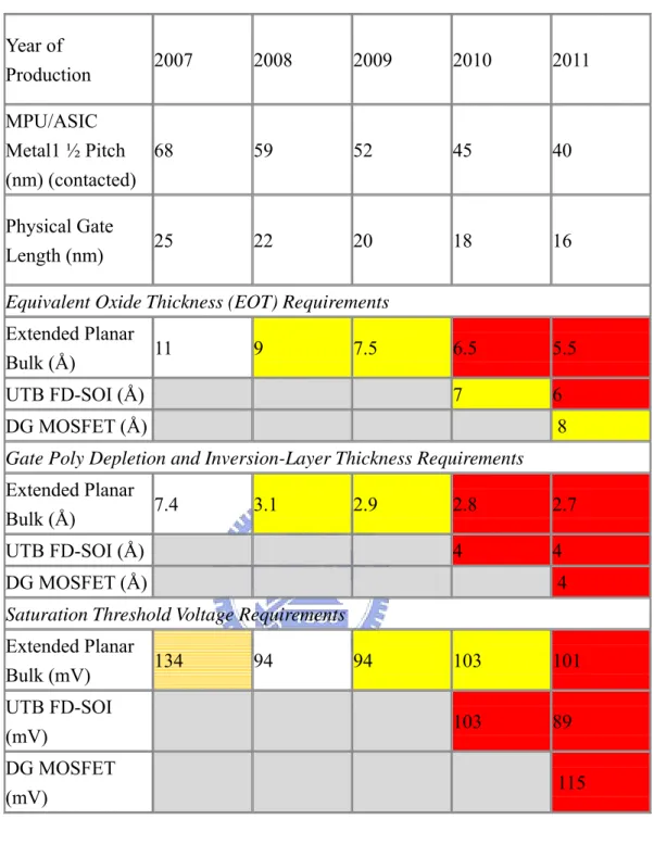
(13) Cox =. ε 0κ. (1.2). tox. where ε 0 is the permittivity of free space, κ is the dielectric constant, tox is the oxide thickness. Therefore, the solution to reduce the tunneling current is to replace SiO2 with a new material of higher dielectric constant. This will keep the same capacitance with thicker layer, which decreases the tunneling current. The new material is so-called “high-κ materials”. It is convenient to define an electrical thickness of the new gate material in terms of its equivalent oxide thickness (EOT) as: EOT =. κ SiO t κd d 2. (1.3). where κ SiO2 is the dielectric constant of SiO2. The parameters κ d and Tphys are the dielectric constant and physical thickness of the gate insulator. The objective is to develop high-κ materials to allow scaling to continue to lower values of EOT. Since the EOT target prescribed by the ITRS in 2008 is only 0.9 nm for 22nm CMOS (Fig. 1-2) [2], the use of high-κ materials is evitable for reducing the leakage current. Many materials are currently under consideration to replace SiO2 as the gate dielectric material for 45 nm node CMOS technology. The requirements to select a suitable high-κ dielectric include: . Moderate κ value: The preferred κ value should be 25-30. There is a trade off with the band gap. Fig. 1-3 shows the κ value varies inversely with the band gap [3]. Thus, materials with extremely large κ value would have a too low band gap, which gives rise 2.
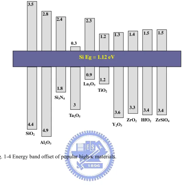
(14) to a too low band offset. In addition, a very large κ is not suitable due to the fringing-induced barrier lowering (FIBL) effect, which causes undesirable large fringing fields at the source and drain junctions [4]. . Band offsets with Si of over 1 eV to minimize carrier injection: High-κ materials should act as a barrier to both electrons and holes. This requires that both their valence and conduction band offsets to Si must be over 1 eV to prohibit conduction by the Schottky emission of electrons or holes. Fig. 1-4 surmises the band offsets of some popular gate dielectric candidates. From the Fig. 1-4, the oxides that satisfy the requirement are Al2O3, ZrO2, HfO2, Y2O3, La2O3, and ZrSiO4.. . Thermal stability on Si when in direct contact with the Si channel: Most high-κ dielectrics are thermally unstable on Si: that is, they react with Si under equilibrium conditions to form a SiO2 or silicate layer at the interface. The interfacial layer would increase the EOT and negate the effect of using high-κ materials. By the condition, the choices of high-κ dielectrics are restricted to very few oxides, such as SrO, Al2O3, ZrO2, HfO2, Y2O3 and La2O3 [5].. Remaining amorphous structure after high temperature process: The gate dielectric must withstand the high temperature process, a rapid thermal annealing (RTA) at 1000oC, 5s. Most metal oxides will crystallize at this temperature, unlike SiO2. In particular, ZrO2 and HfO2 crystallize at mush lower temperature; Al2O3 is amorphous after the RTA but. 3.
(15) has a low κ value; Ta2O5 is also amorphous but is reactive with Si [6]. The crystalline oxide offers a path for leakage current and undesired dopants. It also causes device-to-device variations in leakage, threshold voltage, etc. The incorporation of Si [7] and Al [8] has been proved to prevent the crystallization problem. However, the κ value will decrease as the extent of the incorporation increase. The addition of nitrogen has been found to be beneficial to hafnium silicates to further raise the crystallization temperature [9-11]. . Good interface with Si to retain high mobility: The carrier in the channel is near the dielectric/Si interface, so the interface must keep high quality, in terms of roughness and the absence of interface defects.. . Few defects: The electrically active defects which give rise to energy states in the band gap of oxides are sites of excess or vacancies of oxygen or impurities. These defects might be the starting point of breakdown and cause the device failure. Charge trapped in defects would shift the threshold voltage. The trapped charge changing with time causes the threshold voltage also shift with time. In addition, trapped charge scattering carriers in the channel would lower the mobility [6].. 4.
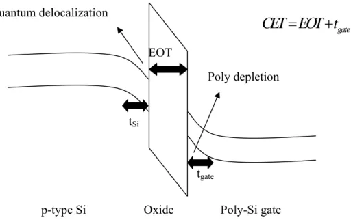
(16) 1.2 Overview of Metal gates Metal gates such as Al were a mainstream of CMOS technology for many years until the need for denser circuits brought about the end of Al gates and the beginning of poly-silicon gate electrodes afforded by self-aligned approach. Today, a transition from the poly-silicon to metal gates is inevitable in high performance devices. Such gate electrodes include many merits of: . No boron penetration: Boron from the poly-silicon gate penetrating to channels through very thin gate dielectric becomes a severe problem, because the high carrier activation in poly-silicon is required to avoid the gate depletion, which causes a positive flat-band voltage (VFB) shift [12].. . Much lower gate resistance: Gate resistance-capacitance (RC) delay becomes a significant concern in designing circuits with very short gates. The low resistivity of metal gates compared to poly-silicon shows the potential to reduce the RC delay.. . No gate depletion length: As shown in Fig. 1-5, the capacitance equivalent thickness (CET) can be defined as:. CET = EOT + t gate + tSi. (1-4). where t gate is the gate depletion depth and tSi arises from quantum delocalization. tSi is intrinsic and cannot easily be removed. On the other hand, t gate (normally 3-5 Å) from the gate depletion can be removed by replacing the poly-silicon with a normal. 5.
(17) metal. Metal electrodes with suitable work functions and sufficient physical and electrical stability are being investigated. According to ITRS (Fig. 1), it can be found that the saturation threshold voltage should be below 0.1 V in 2008. In order to achieve this goal, the preferred work functions should be close to Si conduction band (4.0 eV) for n-MOSFET and Si valance band (5.1 eV) for p-MOSFET to control the threshold voltage. The dependence of the work-function on atomic number is shown in Fig. 1-6 [13] to guide the choice of proper metals. Possible candidates for n-MOSFET are group-IA, group-IIA and Lanthanide elements. The metals in column IA and IIA cannot be used for metal gates because they are very reactive. For p-MOSFET, only Ir (5.27 eV) and Pt (5.65 eV) in the Periodic Table have work function over the desired 5.2 eV. However, Pt is difficult to etch by reactive ion etching (RIE) [14] and Ir will penetrate through the gate dielectric at temperature more than 800oC [15]. Another notable issue for metal gates is that they might react with the gate dielectric at high temperature. This would shift the effective work function towards mid-gap [Fermi thermal]. The solution is to use metal compounds with high thermal stability. TiN [16], TaC [17], and MoOx [18] are all stable enough and investigated widely. Metal alloy systems such as Ni-Ti [19], Ru-Mo [20] are also under consideration. The work function of these alloys can be tuned by changing compositions or employing N, C incorporation. Metal gates can be realized by two integration schemes: gate-first and gate-last. The. 6.
(18) former method is compatible with current poly-silicon gate process flow. Its main disadvantages are [21]: (1) Contamination of front-end tools during processing, (2) Difficult metal etching, and (3) Integrity of gate stack during high-temperature annealing. The gate-last approach is also called a replacement gate technique, where a dummy gate is removed after all doping and high-temperature processes are completed. Its main challenge is the dummy gate stack removal and replacement [21]. Several kinds of gate stack have been developed to realize high-performance CMOS with band-edge work functions for NMOS and PMOS: . Two-metal/one-dielectric: Two different metals with band edge work functions (conduction band edge and valance band edge work functions for NMOS and PMOS, respectively) on the same dielectric.. . One-metal/two-dielectric: One metal with conduction band edge work function on the dielectric for NMOS (PMOS), and dielectric with surface modification for PMOS (NMOS).. . Two- metal/two-dielectric: Two different metals on two different dielectrics.. . FUSI gate: Two FUSI gate with different phases and /or segregated dopants on the same dielectric.. 7.
(19) 1.3 Overview of fully-silicided (FUSI) gates Fully silicided metal gates have received increasing attention in recent years due to the simple integration scheme for implementation and ease of passivation of the underlying gate dielectric. Over the past several years, devices with nickel silicide [22], hafnium silicide [23], platinum silicide [24], and titanium silicide gates [25] were reported. Nickel silicide gates have drawn a lot of attention in recent years due to its mid gap work function, which is necessary to tailor the process to obtain dual work function. It has been shown that the presence of dopants (such as As, P, and B) in poly-silicon can modulate the work function of NiSi gate upon full silicidation. On full consumption of poly-silicon by silicidation, a thin and highly concentrated layer was formed between the metal silicide and gate dielectric. This dopant-rich film at the interface between gate dielectric and metal silicide layer modulates the work function in FUSI gates. The ability to form a pileup of dopant at the silicide/dielectric interface and hence to modulate work function appears to be strongly related to the silicidation conditions. It has been reported that the silicidation temperature and the ratio of Si and Ni thickness determine the phase of the FUSI gate. A two-step RTA FUSI experiment with varying Si:Ni and the temperature of the first step shows formation of different phases of the Ni-Si system. Ni-rich phase does not result in dopant pileup at the Ni3Si2/SiO2 interface. Electrical data corroborates this finding, indicating that phosphorous- or arsenic-doped NMOS and boron-doped PMOS FUSI gates all resulted in the same work. 8.
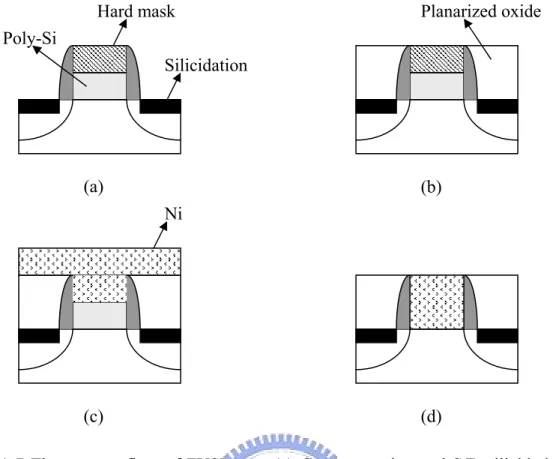
(20) function of ~ 4.65 eV. This likely represents the work function of Ni3Si2 [21]. It has been observed that higher dopant doses give rise to a larger amount of work function shift [26]. This is accompanied by higher amounts of dopant accumulated at the interface between silicide and dielectric [26]. The actual amount and type of dopant accumulated at the silicide/dielectric interface and the phase of the silicide in its immediate vicinity are responsible for setting the work function, while actual experimental conditions, such as dopant dose, energy of implantation, poly-silicon thickness and pre-silicidation annealing might differ. It was observed that the total amount of work function shift saturates at a certain amount of dopant dose. The saturated values of work function shift appear to relate proportionally to the size of the atomic specie of the dopant, the bigger the atom is the larger work function shift attainable [26]. FUSI devices are fabricated using a self-aligned process with independent silicidation of source/drain and the poly-Si gate to avoid thick silicidation in the S/D areas. Fig. 1-7 illustrates the whole process flow. Unlike the common replacement gate approach used for metal gates, this approach retains original dielectric and electrode and only modifies the latter. An alternative and simpler approach to siliciding the gate and source/drain at the same time would require the poly-silicon gate to be substantially thinner than source/drain junction depth, a condition difficult to realize if poly-silicon implantation doping is required.. 9.
(21) 1.4 Fermi-level pinning effect According to the Schottky model, the band alignment is determined solely by the difference between the work function of the metal in vacuum and the electron affinity of Si. However, when a metal is deposited on a dielectric, a lot of energy states form at the interface between the metal and the dielectric. The states in the forbidden band gap of the dielectric are known as metal-induced gap states [27]. They are mainly donor-like from charge neutrality level (ECNL) to EV and acceptor-like from ECNL to EV. The acceptor-like state is neutral when empty and negatively charged when full of electrons, while the donor-like state is neutral when full of electrons and positively charged when empty. Charging of these interface states creates a dipole that tends to drive the band lineup toward a position that would give a zero dipole charge. Hence, the effective work function ( φm ,eff ) is different from the work function in vacuum ( φm ,vac ). Fig. 1-8 illustrates the dipole with negative charge on the dielectric side [28]. The work function change is proportional to the difference between φm,vac and. φCNL ,d [= ( Evac − ECNl ,d ) / q] . Thus, φm ,eff can be expressed as φm ,eff = φCNL ,d + S (φm,vac − φCNL ,d ). (1.4). S and φCNL ,d can be extracted from the experimental φm ,eff − φm,vac plot. When S →0, it means the Fermi level is pinned by charge neutrality level. In contrast, when S→1, it returns to the ideal Schottky case. Typically, the smaller S means the larger Fermi-level pinning [28].. 10.
(22) 1.5 Motivation to use the HfLaON film Hf-based high-κ dielectrics have been recognized as the most promising candidates due to their moderate dielectric constant (~20-25), large energy band gap (5.7 eV), high conduction band offset (1.5 eV), excellent thermal stability on the Si substrate [5, 29, 30]. Hence, Hf-based high-κ dielectrics have been the most popular candidates in recent years, as shown in Fig. 1-7 [31]. However, HfO2 do undergo substantial changes during thermal processing. Dopant activation requires annealing to temperatures of 1000oC or more, much higher than crystallization temperatures of HfO2. The grain boundaries induced by crystallization offer a path for gate leakage current or other undesired dopants to diffuse into gate dielectrics. Several studies have focused on the improvement of the thermal stability of Hf-based dielectrics during the subsequent thermal process. Those studies incorporated Al [8], Si [7], N [9-11] and Ta [32] into HfO2 to form HfO2-based dielectrics, respectively. The incorporation of these elements have been known to retard crystallization of HfO2, but the dielectric constant Si are degraded as the extent of incorporation increases. In addition, the Fermi-level pinning between the metal gate and HfO2 makes it difficult to obtain a CMOS with low threshold voltage [33]. In this thesis, HfLaON is used for the gate dielectrics in the HfSix/Hf0.7La0.3ON/Si n-MOSFET structure. The incorporation of La has been shown to preserve Hf-based dielectric. 11.
(23) from crystallization after 1000◦C RTA, similar to the incorporation of Si. The HfO2 with La also improves significantly the electrical performances of NMOS in terms of drive current with no gate leakage degradation compared to pure HfO2 gate dielectric [34]. Additionally, it has been found that the changing La composition in HfO2 films can effectively tune the work function of the metal gates continuously from Si mid-gap to around 4 eV, which can fit the requirement of NMOS [34]. Therefore, it is worth further studying on the electrical and material characterization of HfLaON.. 1.6 Motivation to use FUSI HfSix gates In this thesis, FUSI HfSix is used for the gate in the HfSix/Hf0.7La0.3ON/Si n-MOSFET structure. Hf has a very low work function of about 4.0 eV and its silicide has an excellent thermal stability up to 950oC [23]. FUSI HfSi gate also shows a low work function value, which is suitable for gate electrode application [23]. Therefore, FUSI HfSix is a promising candidate for dual-metal CMOS process.. 1.7 Thesis organization In this thesis, we used FUSI HfSix as metal gate and Hf0.7La0.3ON as gate dielectric for n-MOSFETs. In chapter 1, a brief review of high-κ/metal gate technology was given to describe their. 12.
(24) application in CMOSFETs. It also shows the motivation to use FUSI HfSix metal gate and Hf0.7La0.3ON dielectrics. In chapter 2, the detailed fabrication process of HfSix/Hf0.7La0.3ON n-MOSFETs and measurement procedure will be described. In chapter 3, the device parameter extraction will be discussed first. Chapter 3.2 and 3.3 shows the results from the measurement and the detailed discussion of characteristics of HfSix/Hf0.7La0.3ON capacitors and n-MOSFETs. From the measurement, low EOT, low effective work function, low threshold voltage, low leakage current and high electron mobility were extracted. It also shows the comparison with other reported n-MOSFETs. Chapter 4 summarizes the findings in this thesis and provides the suggested directions of future studies.. 13.
(25) Fig. 1-1 Leakage current versus gate voltage for various thickness of SiO2 layers [1].. 14.
(26) Year of Production. 2007. 2008. 2009. 2010. 2011. MPU/ASIC Metal1 ½ Pitch 68 (nm) (contacted). 59. 52. 45. 40. Physical Gate Length (nm). 22. 20. 18. 16. 6.5. 5.5. 7. 6. 25. Equivalent Oxide Thickness (EOT) Requirements Extended Planar Bulk (Å). 11. 9. 7.5. UTB FD-SOI (Å) DG MOSFET (Å). 8. Gate Poly Depletion and Inversion-Layer Thickness Requirements Extended Planar Bulk (Å). 7.4. 3.1. 2.9. UTB FD-SOI (Å). 2.8. 2.7. 4. 4. DG MOSFET (Å). 4. Saturation Threshold Voltage Requirements Extended Planar Bulk (mV). 134. 94. 94. UTB FD-SOI (mV). 103. 101. 103. 89. DG MOSFET (mV). 115. Manufacturable solutions exists, and are being optimized Manufacturable solutions are known Interim solutions are known Manufactruable solutions are not known Fig. 1-2 International Technology Roadmap for Semiconductors (ITRS) 2007 for high performance logic technology. [2]. 15.
(27) Fig. 1-3 Static dielectric constant verse band gap for several popular metal oxides [3].. 16.
(28) 3.5 2.8 2.4. 2.3. 1.2. 1.3. 1.4. 1.5. 1.5. 3.4. 3.4. 0.3. Si Eg = 1.12 eV 0.9 1.2 La2O3 1.8. TiO2. Si3N4 3. 3.3 3.6. Ta2O5. ZrO2 HfO2 ZrSiO4 4.4 SiO2. Y2O3 4.9 Al2O3. Fig. 1-4 Energy band offset of popular high-κ materials.. 17.
(29) Quantum delocalization. CET = EOT +tgate +tSi EOT Poly depletion. tSi. tgate p-type Si. Oxide. Poly-Si gate. Fig. 1-5 The three contributions to the capacitance equivalent thickness (CET): gate oxide, poly depletion, and quantum delocalization.. 18.
(30) 6. Pt. EV. Ir. Work Function (eV). 5 Al. 4. EC. Lanthanide Hf. Be Mg. 3. La. Y Ca. Li. Na. 2. Tb. Sr K. Ba. Rb. Yb group-IIA. Cs. Fr. group-IA. 1 0. 0. 10. 20. 30. 40 50 60 70 Atomic Number. 80. Fig. 1-6 The relationship between work function and atomic number. [13]. 19. 90 100.
(31) Hard mask. Planarized oxide. Poly-Si Silicidation. (a). (b) Ni. (c). (d). Fig. 1-7 The process flow of FUSI gate. (a) Gate patterning and S/D silicidation. The hard mask is not removed after pattering so that it can protect the gate from being silicided during the S/D silicidation, (b) Dielectric deposition and planarization, (c) Hard mask removal and Ni deposition, (d) Ni fully silicidation and removal of the remaining Ni.. 20.
(32) Fig. 1-8 Energy band diagram and charging characteristic of interface states for the metal-dielectric system [28].. 21.
(33) Fig. 1-9 Reported high-k materials in recent years. [31]. 22.
(34) Chapter 2 The Experimental Steps and Measurements In this thesis, HfSix/Hf0.7La0.3ON/Si MIS capacitor and transistor were fabricated to investigate their electrical characteristics. The starting wafer was 4-inch, (100) oriented p-type wafer with one side polished. After standard RCA clean (Fig. 2-1), wafers were put into the chamber of the physical vapor deposition (PVD) system, where Hf0.7La0.3O thin films were deposited on the wafers. Subsequently, oxygen post deposition anneal (PDA) was imposed on these samples. After the PDA, a plasma nitridation were imposed on the Hf0.7La0.3O surface wafers to form Hf0.7La0.3ON film. Then, amorphous Si of 5 nm was deposited on the Hf0.7La0.3ON surface followed by a PVD deposition of 20 nm Hf. For the HfSix/Hf0.7La0.3ON/Si MIS capacitor, a 30 nm thick Mo was deposited by PVD to prevent Hf oxidation after the Hf deposition. For HfSix/Hf0.7La0.3ON/Si transistor, an additional amorphous-Si layer of 150 nm was deposited by PVD to avoid ion implantation damage through the gate. Gates of all samples were defined by lithography and etching. After defining the gate, a phosphorous ion implantation at 35 KeV, 5×1015 cm-2 dose was used to form n+ source/drain (S/D) regions of transistors. Afterwards, rapid thermal anneal (RTA) at 1000oC, 5 sec was used to activate carriers in S/D region. The FUSI HfSix gate was. 23.
(35) also formed at this high temperature RTA, which is different from a conventional low temperature FUSI process. For comparison, TaN gates were also deposited on the Hf0.7La0.3ON to form the TaN/Hf0.7La0.3ON/Si MIS capacitor. To analyze the electrical characteristics of these devices, we used HP4156 semiconductor parameter analyzer to measure the I-V characteristics. Besides, the HP4284A precision LCR meter was used to evaluate the C-V characteristic. The whole process is shown in Fig. 2.2 ~ Fig. 2.15.. 24.
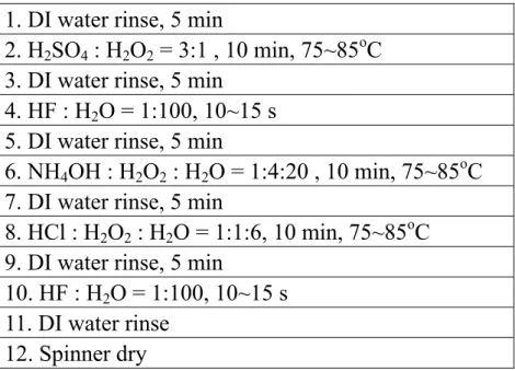
(36) 1. DI water rinse, 5 min 2. H2SO4 : H2O2 = 3:1 , 10 min, 75~85oC 3. DI water rinse, 5 min 4. HF : H2O = 1:100, 10~15 s 5. DI water rinse, 5 min 6. NH4OH : H2O2 : H2O = 1:4:20 , 10 min, 75~85oC 7. DI water rinse, 5 min 8. HCl : H2O2 : H2O = 1:1:6, 10 min, 75~85oC 9. DI water rinse, 5 min 10. HF : H2O = 1:100, 10~15 s 11. DI water rinse 12. Spinner dry Fig. 2-1 Standard RCA clean process.. 25.
(37) Si Fig. 2-2 4-inch (100) P-type wafer.. Si Fig. 2-3 Standard RCA clean.. Hf0.7La0.3O Si Fig. 2-4 Hf0.7La0.3O deposition by PVD.. 26.
(38) O2 PDA. Hf0.7La0.3O Si Fig. 2-5 Low temperature oxygen PDA.. Plasma Nitridation. Hf0.7La0.3O Si Fig. 2-6 Plasma nitridation to form Hf0.7La0.3ON.. 27.
(39) Amorphous Si Hf0.7La0.3ON Si Fig. 2-7 Amorphous Si deposition by PVD (5 nm).. Hf Amorphous Si Hf0.7La0.3ON Si Fig. 2-8 Hf deposition by PVD (20nm).. 28.
(40) Mo Hf Amorphous Si Hf0.7La0.3ON Si Fig. 2-9 Mo deposition by PVD (30 nm) for capacitors.. Amorphous Si. Hf Amorphous Si Hf0.7La0.3ON Si Fig. 2-10 Amorphous Si deposition by PVD (150 nm) for n-MOSFETs.. 29.
(41) MASK. Lithography Patterning. P/R. P/R. Amorphous Si. Mo. Hf. Hf. Amorphous Si. Amorphous Si. Hf0.7La0.3ON. Hf0.7La0.3ON. Si. Si. Fig. 2-11 Lithography patterning for capacitors and n-MOSFETs.. 30.
(42) Etching P/R P/R Amorphous Si Mo Hf. Hf. Amorphous Si. Amorphous Si. Hf0.7La0.3ON. Hf0.7La0.3ON. Si. Si. Fig. 2-12 Etching for capacitors and n-MOSFETs.. 31.
(43) Ion Implantation. Amorphous Si Mo Hf. Hf. Amorphous Si. Amorphous Si. Hf0.7La0.3ON. Hf0.7La0.3ON. S. D Si. Si. Fig. 2-13 Phosphorus ion implantation to form n+ source/drain for n-MOSFETs (35 KeV, 5×1015 cm-2 dose).. 32.
(44) Amorphous Si Mo HfSi. HfSi. Hf0.7La0.3ON. Hf0.7La0.3ON. S. D Si. Si Fig. 2-14 RTA at 1000°C, 5 sec for capacitors and n-MOSFETs.. TaN. Hf0.7La0.3ON Si Fig. 2-15 A TaN gate capacitor for comparison.. 33.
(45) Chapter 3 Result and Discussion 3.1 Device parameter extraction In this thesis, EOT and VFB were extracted from the Quantum C-V simulation. Threshold voltage and mobility extraction was described in detail in the following sections.. 3.1.1 Threshold voltage extraction There are various methods for determining the threshold voltage. Here we use the linear extrapolation method, which is one of the most common techniques to extract the threshold voltage. This method is based on: ID =. W Cox µeff L. VD ⎛ ⎜ VG − Vth − 2 ⎝. ⎞ ⎟ VD ⎠. (3.1). where W and L are channel width and channel length, respectively. Cox is the gate oxide capacitance per unit area and Vth is the threshold voltage. µeff is the field effect mobility, which will be discussed in the next sub-section. The drain current is measured as a function of gate voltage at a low drain voltage = 0.1 V. The low drain voltage is to ensure that the operation is under the linear region. The IDS-VGS curve differs from a straight line at VGS < Vth due to sub-threshold current and at VGS >Vth due to series resistance and mobility degradation. There is a linear region at the neighboring of. 34.
(46) VGS at which gm is maximum. The IDS-VGS curve can be fitted a straight line to extrapolate to ID=0 by means of finding the point of gm, max. Therefore, the Vth is extracted from the VG-axis intersection. The resultant threshold voltage is given by:. Vth = VGSi −. VDS 2. (3.2). where VGSi is the value of the intersection point.. 3.1.2 Mobility extraction According to Eq. (3.1), the effective mobility can be expressed as:. µeff = I D. L CoxW ⎡⎣(VG − Vth ) VD − VD2 / 2 ⎤⎦. (3.3). The effective mobility is usually plotted against an effective normal field Εeff , which is defined as: Εeff =. Vth + 0.2 Vg − Vt + 3tox 6tox. (3.4). 3.2 Characteristics of HfSix/Hf0.7La0.3ON capacitors Fig. 3-1 shows the C-V characteristic of the HfSix/Hf0.7La0.3ON/Si MIS capacitor. The characteristic of the TaN/Hf0.7La0.3ON/Si capacitor is also shown in Fig. 3-2 for comparison. The FUSI HfSix gate was formed by depositing 20 nm Hf on thin 5 nm amorphous-Si followed by 1000oC RTA while the TaN gate was formed by depositing 150 nm TaN directly on Hf0.7La0.3ON. The result shows the HfSix/Hf0.7La0.3ON/Si capacitor has a high capacitance 35.
(47) density, close to that using the TaN gate. This result proves that the FUSI HfSix has no poly-Si depletion. In addition, the VFB of the HfSix gate is more negative than for the TaN gate by 0.05 V, which is needed for low Vth operation. An EOT of 1.2 nm was obtained by the quantum-mechanical (QM) C-V simulation. A low φm ,eff of 4.33 eV was obtained from a VFB-EOT plot for the HfSix/Hf0.7La0.3ON/Si capacitor, as shown in Fig. 3-3. This low effective work function makes them suitable for NMOS applications. In Fig. 3-4, the leakage current of HfSix is 9.2×10⁻⁴ A/cm2 at 1 V below the VFB. It is about 5 orders of magnitude lower than that of SiO2 at a 1.2 nm EOT. This low leakage current is mainly due to the higher dielectric constant of Hf0.7La0.3ON. Hf0.7La0.3ON with higher dielectric constant can have larger physical thickness at the same EOT as SiO2. Therefore, the direct tunneling current can be highly decreased. The low leakage current also proves the good thermal stability of the HfSix/Hf0.7La0.3ON gate structure after a 1000oC RTA. In contrast, the leakage current of TaN is 2.8 × 10⁻³/cm2 at 1 V below the VFB, as shown in Fig. 3-5. The higher leakage current at low voltages using TaN gate than that of HfSix may be due to the sputter-induced damage to the Hf0.7La0.3ON gate dielectric.. 3.3 Characteristics of HfSix/Hf0.7La0.3ON n-MOSFETs Figures 3-6 and 3-7 show the ID-VD and ID-VG transistor of the 1.2 nm EOT HfSix/Hf0.7La0.3ON n-MOSFETs. Good transistor characteristics can be seen from Fig. 3-6. 36.
(48) and 3-7. A small Vth of only 0.18 V was extracted from the linear ID-VG plot, as shown in Fig. 3-8. This is due to the low φm ,eff of 4.33 eV found from the C-V measurements. The mobility as a function of effective electric field for the HfSix/Hf0.7La0.3ON n-MOSFETs is shown in Fig. 3-8. High peak electron mobility of 215 cm2/V-s is obtained at a small EOT of 1.2 nm. Altogether, the small EOT of 1.2 nm, low Vth of 0.18 V, good peak mobility of 215 cm2/V-s and simple high-temperature FUSI processing makes HfSix/Hf0.7La0.3ON device a potential candidate for n-MOSFET application. Table 3-1 summarizes and compares the important transistor characteristics for various FUSI gate/high-κ n-MOSFETs.. 37.
(49) 2.5. o. 2. Capacitance Density (µF/cm ). HfSi 1000 C RTA 2.0 1.5 1.0 0.5 0.0. -2.0. -1.5. -1.0. -0.5. 0.0. 0.5. Gate Voltage (V). Fig. 3-1 C-V characteristics of the HfSix/Hf0.7La0.3ON/Si capacitor.. 38. 1.0.
(50) o TaN 1000 C RTA. 2. Capacitance Density (µF/cm ). 2.5 2.0 1.5 1.0 0.5 0.0 -2.0. -1.5. -1.0. -0.5. 0.0. 0.5. Gate Voltage (V). Fig. 3-2 C-V characteristics of the TaN/Hf0.7La0.3ON/Si capacitor.. 39. 1.0.
(51) φm,eff = 4.33 eV. V. FB. (V). -0.5. -1.0. 0. 1. 2. 3. 4. EOT (nm). Fig. 3-3 VFB-EOT plot of the HfSix/Hf0.7La0.3ON/Si capacitor. The extracted effective work function of HfSix from the plot is 4.33 eV.. 40.
(52) 1. o. HfSix 1000 C RTA. 2. Current Density (A/cm ). 0.1 0.01 1E-3 1E-4 1E-5 1E-6 1E-7 1E-8 1E-9 1E-10 -3.0. -2.5. -2.0. -1.5. -1.0. -0.5. Gate Voltage (V). Fig. 3-4 J-V characteristic of the HfSix/Hf0.7La0.3ON/Si capacitor.. 41. 0.0.
(53) 1. o. TaN RTA 1000 C. Current Density (A/cm). 0.1 0.01 1E-3 1E-4 1E-5 1E-6 1E-7 1E-8 1E-9 1E-10 -3.0. -2.5. -2.0. -1.5. -1.0. -0.5. Gate Voltage (V). Fig. 3-5 J-V characteristic of the TaN/Hf0.7La0.3ON/Si MIS capacitor.. 42. 0.0.
(54) Drain Current (mA). 20. W/L=400/10 um HfSix/Hf0.7La0.3ON. Vg-Vt=2V. 15 Vg-Vt=1.5V. 10 Vg-Vt=1V. 5 Vg-Vt=0.5V. 0 0.0. 0.5. 1.0 1.5 2.0 Drain Voltage (V). Fig. 3-6 ID-VD characteristic of the HfSix/Hf0.7La0.3ON n-MOSFET.. 43. 2.5.
(55) 0. Drain Current (A). 10. -2. 10. -4. 10. HfSix/Hf0.7La0.3ON. -6. 10. Vd=0.1 V -8. 10. -10. 10. -1. 0 1 Gate Voltage (V). Fig. 3-7 ID-VG characteristic of the HfSix/Hf0.7La0.3ON n-MOSFET.. 44. 2.
(56) 0.0014 0.0012. 0.0008. VD= 0.1V. gm. Drain Current (A). 0.0010. Vth=0.18V. 0.0006 0.0004 0.0002 0.0000 -0.5. 0.0. 0.5. 1.0. 1.5. 2.0. Gate voltage (V). Fig. 3-8 ID-VG characteristic of HfSix/Hf0.7La0.3ON n-MOSFETs in linear scale. The extracted Vth is 0.18 V.. 45.
(57) Universal HfSix/Hf0.7La0.3ON. 2. Electron Mobility (cm /V-sec). 600. 400. 200. 0 0.0. 0.2. 0.4. 0.6. 0.8. Effective field (MV/cm) Fig. 3-9 The mobility of the HfSix/Hf0.7La0.3ON n-MOSFET.. 46. 1.0.
(58) Table 3-1 Comparison of device parameters for several FUSI gate/high-κ n-MOSFETs. Ref.. Metal gate. High-κ. Vth (V). EOT (nm). RTA temp.. [35]. FUSI NiSi. La2O3. 0.12. 1.5. 400oC, 30 s. [36]. FUSI YbxSi HfAlON. 0.1. 1.7. Low temp.. [37]. FUSI NiSi2. HfSiON. 0.47. 1.7. 450-650 oC, 1 min. [38]. FUSI NiSi. HfSiON. 0.5. 1.43. Low temp.. [39]. TaN. HfLaON. 0.18. 1.6. 1000oC. This work. FUSI HfSix. HfLaON. 0.18. 1.2. 1000oC, 5 s. 47.
(59) Chapter 4 Conclusion In this thesis, HfSix and Hf0.7La0.3ON have been studied for n-MOSFET applications. This structure has been demonstrated with good device characteristics. We have fabricated the FUSI HfSix gate on Hf0.7La0.3ON with 1.2 nm EOT. After 5 sec, 1000oC RTA, the device displayed a low threshold voltage of 0.18 V, low effective work function of 4.33 eV, low leakage current of 9.2×10⁻⁴ A/cm2 at 1 V and high peak electron mobility of 215 cm2/V-s. Thermal stability at 1000oC RTA ensures that the device can endure the high temperature at the gate-first process. The gate-first and self-aligned process of HfSix/HfLaON n-MOSFETs make this device compatible with current VLSI lines. It has been shown that FUSI HfSix, like FUSI NiSix has a wide range of work-function tuning [23]. The incorporation of n-type dopants to the poly-Si pre-gate has the potential to shift the effect work function to a lower value, which is suitable for NMOS operation. On the other hand, the incorporation of p-type dopants into the poly-Si or phase control technique might be used for PMOS application. The band-edge FUSI HfSix CMOS still needs to be further developed.. 48.
(60) Reference [1] S. –H. Lo, D. A. Buchanan, Y. Yaur, and W. Wang, “Quantum-Mechanical Modeling of. Electron Tunneling Current from the Inversion Layer of Ultra-Thin-Oxide nMOSFET’s,”. IEEE Electron Devices Lett., vol. 18, pp. 209, 1997.. [2] International Technology Roadmap for Semiconductors 2007.. [3] J. Robertson, J. Vac. Sci. Technol., B 18, pp.1785, 2000.. [4] G. C. F. Yeap, S. Krishnan and Ming-Ren Lin, “Fringing-induced barrier lowering (FIBL) in sub-100nm MOSFETs with high-κ gate dielectrics,” IEEE, T-ED, vol. 46, pp. 1537, 1999. [5] K. J. Hubbard and D. G. Schlom, “Thermodynamic stability of binary oxides in contact with silicon,” J. Mat. Res., vol. 11, pp. 2757–2776, 1996.. [6] J. Robertson, “High dielectric constant gate oxides for metal oxide Si transistors.” Rep.. Prog. Phys. 69, pp. 327, 2006.. [7] G. D.Wilk, R. M.Wallace, and J. M. Anthony, “Hafnium and zirconium silicates for advanced gate dielectrics,” J. Appl. Phys., vol. 87, pp. 484, 2000. [8] W. J. Zhu, T. Tamagawa, M. Gibson, T. Furukawa, and T. P. Ma, “Effect of Al inclusion. 49.
(61) in HfO2 on the physical and electrical properties of the dielectrics,” IEEE Electron Device Lett., vol. 23, no. 11, pp. 649, 2002. [9] C. H. Choi, S. J. Rhee, T. S. Jeon, N. Lu, J. H.Sim , R. Clark, M. Niwa, and D. L. Kwong, “Thermally stable CVD HfOxNy advanced gate dielectrics with poly-Si gate electrode,” IEDM Tech. Dig., pp. 857, 2002. [10] A. L. P. Rotondaro, M. R. Visokay, J. J. Chambers, A. Shanware, R. Khamankar, H. Bu, R. T. Laaksonen, L. Tsung, M. Douglas, R. Kuan, M. J. Bevan, T. Grider, J. McPherson, and L. Colombo, “Advanced CMOS transistors with a novel HfSiON gate dielectric,” Symp. VLSI Tech. Dig., pp. 11, 2002. [11] H. S. Jung, Y. S. Kim, J. P. Kim, J. H. Lee, J. H. Lee, N. I. Lee, H. K. Kang, K. P. Suh, H. J. Ryu, C. B. Oh, Y. W. Kim, K. H. Cho, H. S. Baik, Y. S. Chung, H. S. Chang, and D. W. Moon, “Improved current performance of CMOSFETs with nitrogen incorporated HfO2-Al2O3 laminate gate dielectric,” IEDM. Tech. Dig., pp. 853, 2002. [12] Takayuki Aoyama, Kunihiro Suzuki, Hiroko Tashiro, Yoko Tada, and Hiroshi Arimoto, “Flat-band Voltage Shifts in P-MOS Devices Caused by Carrier Activation in P+-Polycrystalline Silicon and Boron Penetration,” IEDM. Tech. Dig., pp. 627, 1997. [13] D. S. Yu, Albert Chin, C. H. Wu, M.-F. Li, C. Zhu, S. J. Wang, W. J. Yoo, B. F. Hung and S. P. McAlister, “Lanthanide and Ir-based Dual Metal-Gate/HfAlON CMOS with Large Work-Function Difference,” IEDM. Tech. Dig., pp. 634, 2005.. 50.
(62) [14] K. C. Chiang, A. Chin, C. H. Lai, W. J. Chen, C. F. Cheng, B. F. Hung, and C. C. Liao, “Very high-κ and high density TiTaO MIM capacitors for analog and RF applications,” Symp. VLSI Tech. Dig., 2005, pp. 62. [15] C. H. Wu, D. S. Yu, A. Chin, S. J. Wang, M.-F. Li, C. Zhu, B. F. Hung, and S. P. McAlister, “High work function IrxSi gates on HfAlON p-MOSFETs,” IEEE Electron Device Lett., vol. 27, no. 2, pp. 90, 2006. [16] S. B. Samavedam, H. H. Tseng, P. J. Tobin, J. Mogab, S. Dakshina-Murthy, L. B. La, J. Smith, J. Schaeffer, M. Zavala, R. Martin, B.-Y. Nguyen, L. Hebert, 0. Adetutu, V. Dhandapani, T-Y.Luo, R. Garcia, P. Abramowitz, M. Moosa, D. C. Gilmer, C. Hobbs, W. J. Taylor, J. M. Grant, R. Hegde, S. Bagchi, E. Luckowski, V. Arunachalam, and M. Azrak, “Metal Gate MOSFETs with HfO2 Gate Dielectric,” Symp. VLSI Tech. Dig., pp. 24, 2002. [17] J.K. Schaeffer, C. Capasso, L.R.C. Fonseca, S. Samavedam, D.C. Gilmer, Y. Liang, S. Kalpat, B. Adetutu, H.-H. Tseng, Y. Shiho, A. Demkov, R. Hegde, W.J. Taylor, R. Gregory, J. Jiang, E. Luckowski, M.V. Raymond, K. Moore, D. Triyoso, D. Roan, B.E. White Jr. , and P.J. Tobin, “Challenges for the Integration of Metal Gate Electrodes,” IEDM. Tech. Dig., pp. 287, 2004. [18] R. Singanamalla, C. Ravit, G. Vellianitis, J. Petry, V. Paraschiv, J.P. van Zijl, S. Brus, M. Verheijen, R.G.R. Weemaes, M. Kaiser, J.G.M. van Berkum, P. Bancken, R. Vos, H.Yu, K. de Meyer, S. Kubicek, S. Biesemans, and J.C. Hooker, “Low VT Mo(O,N) metal gate. 51.
(63) electrodes on HfSiON for sub-45nm pMOSFET Devices,” IEDM. Tech. Dig., pp. 329, 2007. [19] Igor Polishchuk, Pushkar Ranade, Tsu-Jae King, and Chenming Hu, “Dual Work Function Metal Gate CMOS Transistors by Ni-Ti Interdiffusion,” IEEE Electron Device Lett., vol. 23, no. 4, pp. 200, 2002. [20] K. Ohmori, T. Chikyow, T. Hosoi, H. Watanabe, K. Nakajima, T. Adachi, A. Ishikawa, Y. Sugita, Y. Nara, Y. Ohji, K. Shiraishi, K. Yamabe, K. Yamada, “Wide Controllability of Flatband Voltage by Tuning Crystalline Microstructures in Metal Gates Electrodes,” IEDM Tech. Dig., pp. 345, 2007. [21] W.P. Maszara, “Fully Silicided Metal Gates for High-Performance CMOS Technology: A Review,” Journal of the Electrochemical Society, pp. 550, 2005. [22] D. S. Yu, C. H. Wu, C. H. Huang, A. Chin, W. J. Chen, Z. Chunxiang, M. F. Li, and D.-L. Kwong, IEEE Electron Device Lett., 24, pp.739, 2003. [23] C. S. Park, B. J. Cho, and D. L. Kwong, IEEE Electron Device Lett., 25, pp. 372, 2004. [24] T. Nabatame, M. Kadoshima, K. Iwamoto, N. Mise, S. Migita, M. Ohno, H. Ota, N. Yasuda, A. Ogawa, K. Tominaga, H. Satake, and A. Toriumi, IEDM Tech. Dig., pp. 83, 2004. [25] P. Xuan and J. Bokor, IEEE Electron Device Lett., 24, pp. 634, 2003. [26] Jakub Kedzierski, Diane Boyd, Paul Ronsheim, Sufi Zafar, J. Newbury, John Ott, Cyril Cabral Jr., M. Ieong and Wilfried Haenach, “Threshold voltage control in NiSi-gated MOSFETs through silicidation induced impurity segregation (SIIS),” IEDM Tech. Dig., pp.. 52.
(64) 315, 2003. [27] Yee-Chia Yeo, Tsu-Jae King, and Chenming Hu, “Metal-dielectric band alignment and its implications for metal gate complementary metal-oxide-semiconductor technology,” J. Appl. Phys., vol. 92, pp. 7266, 2002. [28] Yee-Chia Yeo, Tsu-Jae King, and Chenming Hu, “Effects of High-κ Gate Dielectric Materials on Metal and Silicon Gate Workfunctions,” IEEE Electron Device Lett., vol. 23, no. 6, pp. 342, 2002. [29] M. Balog, M. Schieber,M. Michman, and S. Patai, “Chemical vapor deposition and characterization of HfO2 films from organo-hafnium compounds,” Thin Solid Films, vol. 41, pp. 247–259, 1977. [30] J. Robertson, “Band offsets of wide-band-gap oxides and implications for future electronic devices,” J. Vac. Sci. Technol. B, vol. 18, pp. 1785–1791, 2000. [31] H. Iwai, S. Ohmi, S. Akama, C. Ohshima, A. Kikuchi, I. Kashiwagi, J. Taguchi, H. Yamamoto, J. Tonotani, Y. Kim, I. Ueda, A. Kuriyama, and Y. Yoshihara, “Advanced Gate Dielectric Materials for sub-100 nm CMOS,” IEDM Tech. Dig., pp. 625, 2002. [32] X. F. Yu, C. X. Zhu, X. P. Wang, M. F. Li, A. Chin, A. Y. Du, W. D. Wang, and D. L.Kwong, “High mobility and excellent electrical stability of MOSFETs using a novel HfTaO gate dielectric,” Symp. VLSI Tech. Dig., pp. 110, 2004. [33] J. C. Phillips, J. Vac. Sci. Technol. B 18, pp. 1749, 2000.. 53.
(65) [34] X. P. Wang, Ming-Fu Li, X. F. Yu, C. Shen, H. H. Ma, Albert Chin, Jiang Ning, M. B. Yu, and Dim-Lee Kwong, “Tuning Effective Metal Gate Work Function by a Novel Gate Dielectric HfLaO for nMOSFETs,” IEEE Electron Device Lett., vol. 27, no. 1, pp.31, 2006. [35] C. Y. Lin, M. W. Ma, Albert Chin, Y. C. Yeo, Chunxiang Zhu, M. F. Li, and Dim-Lee Kwong, “Fully Silicided NiSi Gate on La2O3 MOSFETs,” IEEE Electron Device Lett., vol. 24, no. 5, pp.348, 2003. [36] D. S. Yu, A. Chin, C. H. Wu, M.-F. Li, C. Zhu, S. J. Wang, W. J. Yoo, B. F. Hung, and S. P. McAlister, “Lanthanide and Ir-based dual metal gate/HfAlON CMOS with large work-function difference,” IEDM Tech. Dig., pp. 649–652, 2005. [37] K. Takahashi, K. Manabe, T. Ikarashi, N. Ikarashi, T. Hase, T. Yoshihara, H. Watanabe, T. Tatsumi, and Y. Mochizuki, “Dual workfunction Ni-silicide/HfSiON gate stacks by phase-controlled fullsilicidation (PC-FUSI) technique for 45 nm-node LSTP and LOP devices,” IEDM Tech. Dig., pp. 91–94, 2004. [38] T. Hoffmann, A. Veloso, A. Lauwers, H. Yu, H. Tigelaar, M. Van Dal, T. Chiarella, C. Kerner, T. Kauerauf, A. Shickova, R. Mitsuhashi, I. Satoru, M. Niwa, A. Rothschild, B. Froment, J. Ramos, A. Nackaerts, M. Rosmeulen, S. Brus, C. Vrancken, P. P. Absil, M. Jurczak, S. Biesemans, and J. A. Kittl, “Ni-based FUSI gates: CMOS integration for 45 nm node and beyond,” IEDM Tech. Dig., pp. 269–272, 2006. [39] C. H. Wu, B. F. Hung, A. Chin, S. J. Wang, W. J. Chen, X. P. Wang, M.-F. Li, C. Zhu, Y.. 54.
(66) Jin, H. J. Tao, S. C. Chen, and M. S. Liang, “High temperature stable [Ir3Si-TaN]/HfLaON CMOS with large work-function difference,” IEDM Tech. Dig., pp. 617–620, 2006.. 55.
(67) Vita 姓名:陳冠霖 性別:男 出生年月日:民國 73 年 5 月 12 日 籍貫:台灣省高雄縣 住址:高雄縣大寮鄉永芳村永芳路六鄰 48 之 38 號 學歷:國立清華大學工程與系統科學系 (民國 91 年 9 月~民國 95 年 6 月) 國立交通大學電子研究所固態電子組 (民國 95 年 9 月~民國 97 年 6 月). 論文題目: 使用完全矽化閘極-高介電常數介電質之低臨界電壓金氧半電晶體. A Low Threshold n-MOSFET Using Fully Silicided Gate and High-κ Dielectric. 56.
(68)
數據
![Fig. 1-1 Leakage current versus gate voltage for various thickness of SiO 2 layers [1]](https://thumb-ap.123doks.com/thumbv2/9libinfo/8148257.166988/25.892.166.760.126.699/fig-leakage-current-versus-voltage-various-thickness-layers.webp)
![Fig. 1-3 Static dielectric constant verse band gap for several popular metal oxides [3]](https://thumb-ap.123doks.com/thumbv2/9libinfo/8148257.166988/27.892.150.776.139.731/static-dielectric-constant-verse-several-popular-metal-oxides.webp)
+7
![Fig. 1-6 The relationship between work function and atomic number. [13]](https://thumb-ap.123doks.com/thumbv2/9libinfo/8148257.166988/30.892.202.734.119.526/fig-relationship-work-function-atomic-number.webp)
![Fig. 1-8 Energy band diagram and charging characteristic of interface states for the metal-dielectric system [28]](https://thumb-ap.123doks.com/thumbv2/9libinfo/8148257.166988/32.892.136.789.141.545/energy-diagram-charging-characteristic-interface-states-metal-dielectric.webp)
![Fig. 1-9 Reported high-k materials in recent years. [31]](https://thumb-ap.123doks.com/thumbv2/9libinfo/8148257.166988/33.892.127.800.134.471/fig-reported-high-k-materials-recent-years.webp)
Outline
相關文件
Teachers may consider the school’s aims and conditions or even the language environment to select the most appropriate approach according to students’ need and ability; or develop
vs Functional grammar (i.e. organising grammar items according to the communicative functions) at the discourse level2. “…a bridge between
• Introduction of language arts elements into the junior forms in preparation for LA electives.. Curriculum design for
利用 determinant 我 們可以判斷一個 square matrix 是否為 invertible, 也可幫助我們找到一個 invertible matrix 的 inverse, 甚至將聯立方成組的解寫下.
◦ 金屬介電層 (inter-metal dielectric, IMD) 是介於兩 個金屬層中間,就像兩個導電的金屬或是兩條鄰 近的金屬線之間的絕緣薄膜,並以階梯覆蓋 (step
Then, we tested the influence of θ for the rate of convergence of Algorithm 4.1, by using this algorithm with α = 15 and four different θ to solve a test ex- ample generated as
Numerical results are reported for some convex second-order cone programs (SOCPs) by solving the unconstrained minimization reformulation of the KKT optimality conditions,
Particularly, combining the numerical results of the two papers, we may obtain such a conclusion that the merit function method based on ϕ p has a better a global convergence and
