through a diffusion mechanism or through midgap trap states residing in Ge bulk substrates. © 2007 The Electrochemical Society. 关DOI: 10.1149/1.2734875兴 All rights reserved.
Manuscript submitted December 4, 2006; revised manuscript received February 27, 2007. Available electronically May 10, 2007.
Recently, Ge-channel devices, including bulk Ge,1,2strained Ge,3 and Ge-on-insulator共GOI兲4systems, integrated with high-k gate di-electrics have attracted considerable research interest. Although transistors were originally fabricated on Ge substrates, the lack of a stable Ge native oxide has been an obstacle in complementary-metal-oxide-semiconductor 共CMOS兲 device realization with Ge. Therefore, silicon has been used in CMOS technology for many decades because of the better qualities of its native oxide, such as a low leakage current, low interface state density, and good thermal stability. With the further scaling of device and gate oxide dimen-sions down to the nanometer range, however, the leakage current density in SiO2has become much higher than 2 mA/cm2, which is the maximum concession for low-power applications.5 Conse-quently, higher dielectric constant materials with a thicker physical thickness are being introduced to suppress the concern of excessive gate leakage while maintaining the equivalent oxide thickness 共EOT兲 of the scaled devices.
Presently, hafnium-based oxides or oxynitrides, e.g., HfO2, HfON, and HfSiON, are the uppermost candidates for application among all of the potential high-k dielectrics. Both Si and SiGe metal oxide semiconductor field-effect transistors共MOSFETs兲 integrated with Hf-based gate dielectrics exhibit admirable properties,6-8 but they also reveal undesirable surface carrier mobility degradation behavior.9,10 Changing the substrate from silicon to germanium might be a possible solution to this problem because Ge has a higher carrier mobility relative to that of Si. From recent advances in the deposition of high-k materials, Ge MOSFETs incorporating high-k gate dielectrics have exhibited some promising performance.11,12In this study, we first investigated the physical and electrical character-istics of HfOxNythin films deposited on bulk Ge substrates and then
determined the impact of thermal annealing processing on the entire capacitor structure. Recent reports have described that annealing a cleaned Ge substrate in a NH313 or SiH414 gas ambient, prior to deposition of a high-k dielectric, further improves the MOS proper-ties on Ge. In this paper we describe our investigation of the effects on the passivation efficiency when using NH3plasma on a Ge sub-strate. We found that the overall MOS structures had higher thermal stability and showed improved electrical characteristics. In addition, we provide a scheme outlining the charge trapping mechanism.
Experimental
Metal–insulator–semiconductor共MIS兲 capacitors were fabricated on n-type Ge substrates共resistivity ⬃8–12 ⍀ cm兲, which were
pre-cleaned through a cyclic rinse involving a diluted HF dip and deion-ized water. After wet cleaning, the NH3plasma exposure on the Ge surface of some samples was performed in the plasma-enhanced chemical vapor deposition共PECVD兲. HfOxNythin films were
sub-sequently deposited through reactive sputtering in a Ar + N2 ambi-ent with a pure Hf target, followed by annealing in a N2atmosphere containing residual oxygen; various postdeposition annealing tem-peratures 共500 and 600°C兲 and durations 共30 s and 5 min兲 were employed. Next, a platinum共Pt兲 dot was deposited using electron beam evaporation through a shadow mask. For evaluating the ther-mal stability of the Pt/high-k/Ge structures, the annealing conditions described above were performed after metallization. The detailed deposited conditions and fabrication procedures have been described previously.15 Transmission electron microscopy 共TEM兲 and secondary-ion mass spectroscopy共SIMS兲 were employed to inves-tigate the entire structure and Ge incorporation behavior, respec-tively. In addition, we carried out ex situ XPS measurements using an Al K␣ source 共1486.6 eV兲 to examine the effects of surface plasma nitridation on the dielectric-substrate interface and evaluate the Ge contamination level within the top high-k films. In electrical characterization, the capacitance-voltage 共C-V兲 and conductance-voltage共G-V兲 curves were measured using an HP4284 LCR meter, while the current-voltage共I-V兲 characteristics were measured using a Keithley 4200 semiconductor analyzer system. We further ex-tracted the series resistance and external inductance or capacitance in measurements and then applied as a correction to the measured capacitance and conductance.16,17The value of the effective trapped charge density 共Neff兲 was determined quantitatively by measuring the hysteresis width at flatband voltage 共VFB兲 in the bidirectional 共C-V兲 sweeps.18
The interface state density共Dit兲 was estimated from both high-low frequency capacitance method19and the共G-V兲 char-acteristics using Hill’s method.20
Results and Discussion
TEM image and SIMS depth profiles.— Figure 1 shows
cross-sectional TEM image of as-deposited Pt/HfOxNy/Ge structure. We
characterized that the thicknesses of the HfOxNy bulk film and the
interfacial layer 共IL兲 were ca. 73 and 19 Å, respectively. When HfOxNy/Ge system undergoes high-temperature process, of primary
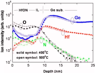
interest is the resultant germanium diffusion in the overlying HfOxNyfilms. As the SIMS depth profiles illustrated in Fig. 2, we
observed a large Hf tail, a known SIMS artifact, at the end of the HfOxNylayer, and ion yield enhancements of both Ge and Hf at the beginning of the Ge substrate. Discarding these artificial phenom-ena, a U-shaped distribution of Ge did exist inside the overlying
HfOxNy layer. From the concentration levels, we suggest that the
higher thermal annealing indeed enhanced the incorporation of Ge, relative to the concentration in low-temperature processed sample. Assuming that the composition is the mixture of HfOxNy and
GeOxNy, we evaluated the amount of incorporated Ge quantitatively
through X-ray photoelectron spectroscopy共XPS兲 measurements be-cause of the lack of sputtering yield information for Ge in the HfOxNy layer. Considering the respective atomic sensitivity factors of the Ge 2p3, Hf 4f, O 1s, and N 1s core levels, we estimated an average Ge concentration of ca. 12共±1.4兲 atom % in their overlying high-k layers for the 400°C processed sample, with the values in-creasing to ca. 19.3共±2兲 atom % after 500°C PDA for 5 min. Such a low-temperature annealing has led to severe Ge incorporation into the HfOxNydielectric film. Note that the maximum sampling depth is ca. 45 Å in Ge 2p3 spectrum, and it exactly involves in a U-shaped distribution of Ge within the high-k films, therefore, we use an average value for evaluating the Ge contamination. These Ge
atoms are incorporated in the form of GeOx through both external
and internal contamination mechanisms. A higher surface concentra-tion of Ge oxide in the SIMS analyses has been identified as arising from gaseous GeO species diffusing out from the substrate and downward into the high-k layer via airborne transportation; the con-tamination depth has been estimated to be ca. 20 Å, at least for
high-k thin films deposited on Ge substrates.21This kind of surface con-tamination, however, can be further suppressed by capping a thick SiO2layer onto the back side of the Ge substrate prior to performing the annealing process. In addition, bulk contamination of GeOxmay
result from the desorption of a defective GeOx-containing IL and/or
the oxidation of the Ge substrate due to residual oxygen existing in a N2ambient.15
Capacitance and conductance characteristics of high-k/Ge MIS capacitor.— Figure 3 displays multifrequency C-V characteristics of
Pt/HfOxNy/Ge capacitors before and after performing the
postdepo-sition annealing共PDA兲 and postmetallization annealing 共PMA兲, re-spectively. Note that the sweep direction in all of the curves pre-sented here is from strong accumulation to strong inversion and they seem not to reach full saturation in the accumulation regimes. This phenomenon can be reasonably understood in term of fast detrap-ping of the trapped charges during the C-V sweep; on the contrary, when the voltage is swept from inversion to accumulation, the nor-mal saturation behavior in C-V curves can be seen. Here, we ex-tracted the capacitance-equivalent-thickness共CET兲 at a value of Vg of +2 V in the C-V curves was ca. 28 Å for as-deposited sample; it decreased to ca. 27 and 26 Å after PDA and PMA, respectively. Extending the annealing duration to 5 min leads to further CET reduction of ca. 23 Å共not shown here兲, and it partly arises from the shrinkage of the IL15due to the fact that Ge does not prefer to form the germinate HfGeO4,22,23unlike Si, which readily forms HfSiO4, through reaction with Hf. In addition, we observed that the C-V stretch-out behavior with the hump emerged in depletion for all samples, indicating the existence of a large density of interface states at the dielectric interface. Considering the frequency depen-dence of the interface properties, the deviation of the 10 kHz curve with respect to the 1 MHz curve was obviously abated by perform-ing subsequent annealperform-ing processes. In particular, the PMA-processed sample revealed a deeper “dip” in depletion, indicative of its improved interface quality. The quantitative analyses of the Dit showed that the as-deposited HfOxNy/Ge gate stack revealed a large value of Ditof ca. 8⫻ 1012cm2.eV−1and it reduced to the value of
Ditof ca. 3.5⫻ 1012and ca. 1.4⫻ 1012cm2.eV−1for the PDA and PMA samples, respectively. Interface traps and dangling-bond de-fects existing in near-interfacial Ge oxide or Ge oxynitride have
Figure 1. Cross-sectional TEM image of as-deposited Pt/HfOxNy/Ge gate stack.
Figure 2. 共Color online兲 SIMS profiles of as-deposited HfOxNy/Ge gate stack after two different annealing conditions: 共a兲 400°C, 30 s and 共b兲 500°C, 5 min
Figure 3. 共Color online兲 Multifrequency C-V curves of Pt/HfOxNy/n–Ge capacitors measured at共䉱兲 10 kHz, 共•兲 100 kHz, and 共䊏兲 1 MHz: 共a兲 as-deposited,共b兲 500°C PDA, 30 s, and 共c兲 500°C PMA, 30 s.
been characterized in the HfO2/Ge system.24Recently, Chui et al. also examined that the level of Dit was quite high and still on the order of 1012cm2.eV−1for GeO
xNy/Ge gate stack even though
re-ceiving forming-gas anneal共FGA兲.25As a result, we believe that a higher value of Ditpresented at the HfOxNy/Ge interface should be associated with poor quality of the defective GeOxIL.
Figure 4 presents the corresponding G-V curves of Pt/HfOxNy/Ge gate stacks measured at 100 kHz; the result of
Pt/HfOxNy/Si control sample is also shown for comparison. The
G-V traces obviously exhibit an interface loss peak, corresponding
to the hump observed in C-V depletion. The PMA process reduced the conductance peak that emerged in the G-V curve of the as-deposited sample to a greater extent than did the PDA process, which is consistent with the examination of Dit. Another noteworthy feature is that we measured a high value of conductance in inversion and it displayed gate-bias independence; this finding is rare for tra-ditional Si MOS capacitors.26Generally, the equivalent parallel con-ductance passes through a peak in weak inversion and drops imme-diately to a very low value in strong inversion; in other words, an exponential decline of the conductance values should occur, like Si case shown here. In contrast, we observed gate-bias-independent conductance in inversion in our case, suggesting that the minority carriers in the Ge substrate, formed either through the generation/ recombination via midgap trap levels or through a diffusion mecha-nism, do indeed contribute an energy loss in inversion and compete with interface-state loss in depletion.27Fukuda et al. have investi-gated the GeOxNy/Ge interface properties through the conductance method28and they also simultaneously explored the identical inver-sion conductance.29We have observed the anomalous G-V charac-teristics on low-doped共ca. 1014cm−3兲 Ge substrate for both types; this behavior can be minimized by increasing dopant concentration. Chui et al. characterized the gate-bias-independent conductance in inversion for MOS capacitors with GeOxNy dielectric thin film on
n-type 共ca. 1016cm−3兲 Ge substrate, but not on p-type 共ca. 5 ⫻ 1017cm−3兲 Ge substrate.25 We suggest that the onset of this strange behavior in Ge capacitor is strongly dependent on the sub-strate doping level because this in turn determines the amount of minority carrier and corresponding response time. Moreover, we no-ticed that the measured capacitance and conductance rose after dif-ferent thermal processes, which are a typical characteristic of the increased number of bulk traps, presumably caused by impurity at-oms introduced during high-temperature annealing. These induced
bulky defects in Ge, with energy levels near the midgap, not only contribute to greater bulk trap loss but also enhance the supply of minority carriers to the inversion layer, incurring the low-frequency-like behavior in the 10 kHz C-V curves. We suggest that both ther-mal mechanisms are significant in Ge because of a large intrinsic carrier concentration 共ca. 2 ⫻ 1013cm−3兲 because they obviously affect the room-temperature C-V characteristics measured at high frequencies, even as high as 1 MHz.30
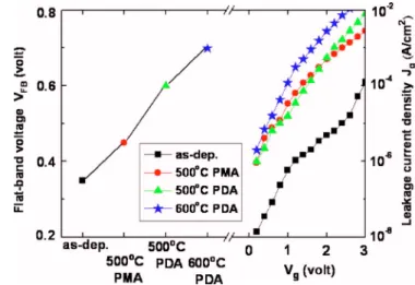
Flatband voltage shift and gate leakage characteristics.— As
indicated in Fig. 5, we examine the variation of the VFBshift共the left-hand axis兲 and the gate leakage current Jg共the right-hand axis兲 with respect to the annealing temperature. It can be seen that the value of VFBfor the as-deposited sample共ca. 0.35 V兲 is lower than the value of the ideal work-function difference共ca. 0.9 eV兲 between a Pt gate and n-Ge substrate, implying that a substantial number of positive charges have been introduced into the gate dielectric/IL bi-layer. High temperature annealing caused the positive shift of the
VFBand increased the Jgconsiderably to 1⫻ 10−3A/cm2at共VFB + 1兲 V after 600°C PDA; these behaviors are possibly correlated with the degree of GeO volatilization. As far as the positive VFB shift after thermal annealing is concerned, the desorption process of GeO is believed to generate additional negative charges and leads to charge neutralization. Bai et al. have examined that an increase of PMA temperature made the value of VFB shift positively and they interpreted this phenomenon in terms of the out-diffusion of GeOx
from Ge substrate.31Another result demonstrated further by Wu et al. was that the thicker the Si layer capping onto Ge substrate is, the smaller the amount of Ge out-diffusion is. Accordingly, a less posi-tive VFBshift was found owing to the reduction of these negative charges.32Furthermore, more severe out-diffusion of GeO was seen upon increasing annealing temperature; this in turn caused the
high-k/Ge interface degradation.22This tendency is obviously different from that observed in the Pt/HfOxNy/Si capacitors which depict the
reduction in Jgupon increasing PDA temperature. We thus suggest that the GeOx incorporation into the overlying HfOxNy bulk film may form the leakage path and contribute to gate leakage current, especially after annealing at 600°C.
Influence of NH3plasma passivation on high-k/Ge MIS
proper-ties.— Most studies have demonstrated that the gate leakage current
in high-k/Ge systems decreases significantly after receiving surface thermal-annealing in a NH3ambient, especially prior to the deposi-tion of HfO2 dielectric films.33 We observed similar effects after NH3plasma, as presented in the inset of Fig. 6. The gate leakage
Figure 4. 共Color online兲 Typical 100 kHz G-V curves of as-deposited and
annealed Pt/HfOxNy/n–Ge capacitors共solid symbols兲; the annealing duration is 30 s for these two thermal processes. Note that the G-V curve of as-deposited Pt/HfOxNy/n–Si capacitor共open squares兲 is added for comparison.
Figure 5.共Color online兲 The VFBshift共the left y-axis兲 and I-V characteris-tics共the right y-axis兲 of Pt/HfOxNy/n–Ge capacitors subjected to different thermal processing.
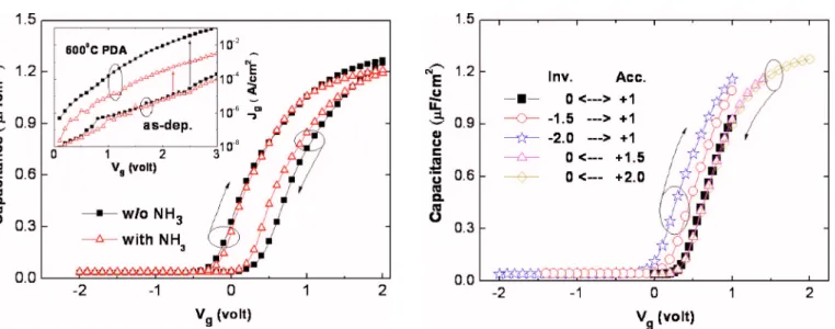
was lower after higher-temperature PDA for the NH3-treated sample relative to that of the HF-last sample. Moreover, plasma treatment reduced the hysteresis loop in the bidirectional C-V curves measured at 1 MHz共Fig. 6兲; reduction of the interface state density to the order of 1011cm2.eV−1was also achieved. We obtained a corre-sponding value of Neffof ca. 4.8⫻ 1012cm−2 for HF-last sample and it decreased to ca. 2.5⫻ 1012cm−2after surface nitridation. It was believed that substoichiometric oxide may create a high density of charge-trapping sites at the dielectric-substrate and they could induce charge trapping and detrapping. The formation of Ge–N chemical bonds and the inhibited growth of GeOx共x ⬉ 2兲 may be responsible for the resulting improved electrical performance. The interposed GeOxNy IL may behave as a diffusion barrier and sup-press the volatilization of GeO out-diffusion from Ge substrate; therefore, causing a less significant increase in Jgafter NH3plasma pretreatment.
On the other hand, to obtain a deeper insight into the origin of the hysteresis behavior, we separately extended the inversion and accumulation biases in the C-V sweeps and found that the increased inversion bias did lead to an increased hysteresis width, but the increased accumulation bias did not, as is evident in Fig. 7. This fact implies that hole trapping is the dominant mechanism; the scheme of a charge trapping model for a Pt/HfOxNy/GeOx/Ge gate stack has
been proposed in other studies.34 We conclude that the minority carriers共in this case, holes for n-type Ge兲 tunnel from the Ge sub-strate and become trapped at the inner-interface and/or inside the deficient GeOxinterlayer. This process causes the C-V curve to shift negatively with the deviation of the VFBwhen the sweeping bias is started further from the negative side, i.e, more inversion charges are trapped. In contrast, the C-V curve exhibits its own value of VFB without being trapped when the voltage is swept from accumulation to inversion.
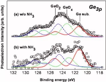
XPS analysis of Ge interface chemistry through NH3plasma
ni-tridation.— In Fig. 8 and 9 we investigate the distribution of GeO
species in entire structures through analyses of the Ge 2p3 and Ge 3p core levels, a broad band consisting of Ge dioxides and subox-ides and elemental Ge. We compared the spectra of these two Ge photoemissions because they allow sampling at significantly differ-ent depths. We employed mixed Gaussian-Lordiffer-entzian line shapes to reproduce these two Ge core levels from three components, Ge, GeO, and GeO2. From the high-surface-sensitivity Ge 2p3 spectrum 共Fig. 8兲, a quite high intensity ratio of the GeO2and GeO to the Ge
substrate was found for both samples; this feature arose primarily from the surface contamination of GeOx 共x ⬉ 2兲. The average Ge
concentration estimated within the top of high-k bulk layer is ca. 12共±1.4兲 atom % for HF-last sample; with the value can be reduced to ca. 4.8 atom % providing that the Ge substrate receives surface pretreatment of NH3 plasma. Subsequently annealing the NH3 sample at 600°C for 30 s causes the Ge concentration increasing to the value of ca. 14 atom %. From the concentration levels, we found that NH3pretreatment did assist to minimize Ge incorporation be-havior during annealing with respect to the result obtained in HF-last sample that the Ge contamination was up to ca. 19.3共±2兲 atom % after annealing at 500°C for 5 min. However, we suggest that the finite improvements in characteristics of NH3-treatment samples as compared to the literatures14,32using another passivation technique, the Si interlayer on Ge, can be attributed to the incomplete passiva-tion of the dangling bonds on the Ge surface; such a surface would not fully diminish the formation of GeOx. Lower dissociated
tem-Figure 6. 共Color online兲 Bidirectional sweep 共1 MHz兲 C-V curves of
Pt/HfOxNy/n–Ge capacitors prepared共䊏兲 without and 共䉭兲 with NH3 nitri-dation. The inset displays the corresponding plots of Jgvs Vgbefore and after PDA at 600°C.
Figure 7. 共Color online兲 Dependence of the hysteresis width in C-V
共1 MHz兲 sweep on the starting accumulation and inversion gate biases; the absence of the hysteresis behavior in the gate-bias ranged from 0 to 1 V.
Figure 8.共Color online兲 Ge 2p3 XPS spectra of Pt/HfOxNy/n–Ge capacitors prepared without and with NH3 nitridation. Three components were ex-tracted: Ge, GeOx, and GeO2.
perature共ca. 500°C兲 of Ge–N bonds35is a major cause to result in a still higher concentration of Ge observed after high-temperature pro-cessing.
In contrast, the Ge 3p spectrum共Fig. 9兲 clearly demonstrated that the intensity from the GeOx共x ⬉ 2兲 was lower than that from the
substrate after NH3 plasma nitridation, especially for inhibiting a large amount of Ge suboxides; these phenomena are the opposite of that observed for the non-nitrided high-k/Ge sample. Our explana-tion for this experimental finding is that the Ge 3p core level is capable of examining the amount of Ge oxide existing at the
high-k/Ge interface because it possesses a higher sampling depth 共ca.
80 Å兲 relative to that 共ca. 34 Å兲 of the Ge 2p3 spectrum.36 Accord-ingly, such a low oxide/substrate emission ratio after performing the nitridation process is a direct result of NH3 plasma pretreatment diminishing the number of GeOx共x ⬉ 2兲 defects at the interface; in
other words, the reduced charge trapping centers is achieved. These results also imply that surface nitridation does indeed assist in en-hancing the thermal stabilities of Pt/HfOxNy/Ge MOS structures.
Conclusions
In this study, we performed the physical and electrical analyses to systematically examine the HfOxNy thin films sputtered on Ge
substrates and the admittance properties of their MIS capacitors. We observed a U-shaped distribution of Ge atoms into the overlying HfOxNydielectric and an increased Ge incorporation共⬎17 atom %兲
after higher thermal processing. Although high-temperature anneal-ing did improve the interface qualities, they also caused a positive shift of the VFB, severe charge trapping, and increased Jg consider-ably; which are closely related to the existence of GeOx defective layer and the degree of resultant GeO desorption. These problems could be relieved after performing NH3plasma pretreatment on the Ge surface; in particular, suppressing the amount of Ge incorpora-tion 共⬍5 atom %兲 and the substoichiometric oxide at dielectric– substrate interface. We suggested that the surface nitridation process indeed diminished the volatilization of gaseous GeO and enhanced the thermal stability of the high-k/Ge interface. Additionally, we measured a high loss in the parallel conductance in the inversion region and it revealed gate-bias independence, implying the fast generation rate of minority carriers in Ge through either a diffusion mechanism or bulk traps within the substrates.
D. L. Kwong, in Technical Digest of the Symposium. VLSI, p. 119共2003兲. 5. http://public.itrs.net
6. O. Weber, F. Andrieu, M. Cass, T. Ernst, J. Mitard, F. Ducroquet, J.-F. Damlen-court, J.-M. Harmann, D. Lafond, A.-M. Papon, L. Militaru, L. Thevenod, K. Romanjek, C. Leroux, F. Martin, B. Guillaumot, G. Ghibaudo, and S. Deleonibus, Tech. Dig. - Int. Electron Devices Meet., 2004, 867.
7. C. S. Kang, H.-J. Cho, K. Onishi, R. Choi, R. Nieh, S. Gopalan, S. Krishnan, and J. C. Lee, in Technical Digest of the Symposium, VLSI, p. 146共2002兲. 8. H. C.-H. Wang, C.-W. Tsai, S.-J. Chen, C.-T. Chan, H.-J. Lin, Y. Lin, H.-J. Tao,
S.-C. Chen, C. H. Diaz, T. Ong, A. S. Oates, M.-S. Liang, and M.-H. Chi, in Technical Digest of the Symposium, VLSI, p. 170共2005兲.
9. A. L. P. Rotondaro, M. R. Visokay, J. J. Chambers, A. Shanware, R. Khamankar, H. Bu, R. T. Laaksonen, L. Tsung, M. Douglas, R. Kuan, M. J. Bevan, T. Grider, J. Mcpherson, and L. Colombo, in Technical Digest of the Symposium, VLSI, p. 148 共2002兲.
10. T. Yamaguchi, R. Iijima, T. Ino, A. Nishitama, H. Satake, and N. Fukushima, Tech. Dig. - Int. Electron Devices Meet., 2002, 621.
11. M. Houssa, T. Conard, F. Bellenger, G. Mavrou, Y. Panayiotatos, A. Sotiropoulos, A. Dimoulas, M. Meuris, M. Caymax, and M. M. Heynsa, J. Electrochem. Soc.,
153, G1112共2006兲.
12. S. Zhu, R. Li, S. J. Lee, M. F. Li, A. Du, J. Singh, C. Zhu, A. Chin, and D. L. Kwong, IEEE Electron Device Lett., 26, 81共2005兲.
13. N. Lu, W. Bai, A. Ramirez, C. Mouli, A. Ritenour, M. L. Lee, D. Antoniadis, and D. L. Kwong, Appl. Phys. Lett., 87, 051922共2005兲.
14. N. Wu, Q. Zhang, C. Zhu, D. S. H. Chan, A. Du, N. Balasubramanian, M. F. Li, A. Chin, and J. K. O. Sin, IEEE Electron Device Lett., 25, 631共2004兲.
15. C.-C. Cheng, C.-H. Chien, C.-W. Chen, S.-L. Hsu, C.-H. Yang, and C.-Y. Chang, J. Electrochem. Soc., 153, F160共2006兲.
16. W. H. Wu, B. Y. Tsui, Y. P. Huang, F. C. Hsieh, M. C. Chen, Y. T. Hou, Y. Jin, H. J. Tao, S. C. Chen, and M. S. Liang, IEEE Electron Device Lett., 27, 399共2006兲. 17. H.-T. Lue, C.-Y. Liu, and T.-Y. Tseng, IEEE Electron Device Lett., 23, 553共2002兲. 18. M.-K. Lee, C.-F. Yen, J.-J. Huang, and S.-H. Lin, J. Electrochem. Soc., 153, F266
共2006兲.
19. D. K. Schroder, Semiconductor Material and Device Characterization, 2nd ed., 368, John Wiley & Sons, Inc., New York共1998兲.
20. W. A. Hill and C. C. Coleman, Solid-State Electron., 23, 987共1980兲.
21. Q. Zhang, N. Wu, D. M. Y. Lai, Y. Nikolai, L. K. Bera, and C. Zhu, J. Electrochem. Soc., 153, G207共2006兲.
22. C.-C. Cheng, C.-H. Chien, J.-H. Lin, C.-Y. Chang, G.-L. Luo, C.-H. Yang, and S.-L. Hsu, Appl. Phys. Lett., 89, 012905共2006兲.
23. P. M. Lambert, Inorg. Chem., 37, 1352共1998兲.
24. V. V. Afanas’ev, Y. G. Fedorenko, and A. Stesmans, Appl. Phys. Lett., 87, 032107 共2005兲.
25. C. O. Chui, F. Ito, and K. C. Saraswat, IEEE Trans. Electron Devices, 53, 1501 共2006兲.
26. D. Flandre, F. Campabadal, J. Esteve, E. Lora-Tamayo, and F. V. D. Wiele, J. Appl. Phys., 70, 5111共1991兲.
27. E. H. Nicollian and J. R. Brews, MOS (Metal Oxide Semiconductor) Physics and Technology, John Wiley & Sons, Inc., New York共1982兲.
28. Y. Fukuda, T. Ueno, and S. Hirono, Jpn. J. Appl. Phys., Part 1, 44, 7928共2005兲. 29. Y. Fukuda, T. Ueno, S. Hirono, and S. Hashimoto, Jpn. J. Appl. Phys., Part 1, 44,
6981共2005兲.
30. A. Dimoulas, G. Vellianities, G. Mavrou, E. K. Evangelou, and A. Sotiropoulos, Appl. Phys. Lett., 86, 223507共2005兲.
31. W. P. Bai, N. Lu, and D.-L. Kwong, IEEE Electron Device Lett., 26, 378共2005兲. 32. N. Wu, Q. Zhang, D. S. H. Chan, N. Balasubramanian, and C. Zhu, IEEE Electron
Device Lett., 27, 479共2006兲.
33. N. Wu, Q. Zhang, C. Zhu, C. C. Yeo, S. J. Whang, D. S. H. Chan, M. F. Li, B. J. Cho, A. Chin, D.-L. Kwong, A. Y. Du, C. H. Tung, and N. Balasubramanian, Appl. Phys. Lett., 84, 3741共2004兲.
34. C.-C. Cheng, C.-H. Chien, G.-L. Luo, C.-H. Yang, M.-L. Kuo, J.-H. Lin, and C.-Y. Chang, Appl. Phys. Lett., 90, 012905共2007兲.
35. K. Prabhakaran and T. Ogino, Surf. Sci., 387, L1068共1997兲.
36. NIST Electron Inelastic-Mean-Free-Path Database 71共Version 1.1兲, National Insti-tute of Standards and Technology共2000兲.
Figure 9.共Color online兲 Ge 3p XPS spectra of Pt/HfOxNy/n–Ge capacitors prepared without and with NH3 nitridation. Three components were ex-tracted: Ge, GeOx, and GeO2.