Significant Improvement of GaN Crystal Quality with Ex-situ
Sputtered AlN Nucleation Layers
Shuo-Wei Chen
1),2), Young Yang
2), Wei-Chih Wen
2), Heng Li
1), and Tien-Chang Lu
1)*
1) Department of Photonics, National Chiao Tung University, No.1001, Daxue Rd., East Dist.,
Hsinchu 300, Taiwan
2) Epistar Corporation, No.5, Lixing 5th Rd., East Dist., Hsinchu 300, Taiwan
*Corresponding author. E-mail address:
[email protected]
;
Tel.: +886-3-5131234; fax: +886-3-5727981
ABSTRACT
Ex-situ sputtered AlN nucleation layer has been demonstrated effective to significantly improve crystal quality and electrical properties of GaN epitaxy layers for GaN based Light-emitting diodes (LEDs). In this report, we have successfully reduced X-ray (102) FWHM from 240 to 110 arcsec, and (002) FWHM from 230 to 101 arcsec. In addition, reverse-bias voltage (Vr) increased around 20% with the sputtered AlN nucleation layer. Furthermore, output power of LEDs grown on sputtered AlN nucleation layer can be improved around 4.0% compared with LEDs which is with conventional GaN nucleation layer on pattern sapphire substrate (PSS).
Keywords: light-emitting diodes (LEDs), AlN, internal quantum efficiency (IQE), multiple quantum wells (MQWs),
sputter
1. INTRODUCTION
There are several significant factors which affect quantum efficiency in GaN based light-emitting diodes (LEDs) and crystal quality is always the most important. GaN-based LED structures are made typically on the (0001) c-plane sapphire substrates because of no nature GaN substrates.1, 2 Several reports showed that interfacial energy difference
between sapphire and GaN film may cause dislocations which can produce V-shape pits and lower crystal quality of the subsequently grown GaN layer.3 Furthermore, efficiency is also reduced by nonradiative recombination centers caused
by poor quality of GaN layers.4 For solving interfacial problem, an in-situ low temperature GaN nucleation layer is
inserted in order to decrease the energy difference from thermal expansion coefficient and lattice constant mismatch between sapphire substrates and GaN. To reduce threading dislocation densities (TDDs) is another way to improve the GaN crystal quality, and epitaxially lateral over-growth,5, 6 insertion of superlattice layers or SiN
successful methods of TDD reduction. After that, patterned sapphire substrates (PSS) are widely used on GaN based LEDs because the TDDs can be well limited, and high internal quantum efficiency (IQE) can be achieved.9 Moreover, the light extraction efficiency can be significantly enhanced because of rough interfaces between sapphire and GaN.
Recently, for the purpose of achieving better electrical performance of LEDs, ex-situ sputtered AlN nucleation layer on PSS has been demonstrated to improve crystal quality and electrical properties of GaN epitaxy layers for GaN based LEDs.10 The improvement could be owing to the fact that ex-situ sputtered AlN nucleation layer has better coverage on sapphire substrates and could lower the lattice constant mismatch between sapphire and the GaN film. However, large strain still exists in the LED structure and may lead to cracks within GaN layers because of different lattice constants and thermal expansion coefficients between GaN and sapphire substrate. The internal electric field caused by strain may induce band bending and suppress the recombination efficiency between electrons and holes in the multiple quantum wells (MQWs) based on the strain-related quantum-confined Stark effect (QCSE).11-13 Therefore, relationship of strain, crystal quality and electrical properties is going to be discussed.
2. EXPERIMENT 2.1 Substrates and precursors
Trimethylgallium (TMGa), trimethylaluminium (TMAl), trimethylindium(TMIn), and ammonia (NH3) were used as
precursors of chemical reactions for Ga, Al, In, and N sources, respectively. N-type and p-type doping sources were silane (SiH4) and bicyclopentadienyl magnesium (Cp2Mg), respectively. The GaN based LED structures were grown on
4-inch (0001) PSS by MOCVD.
2.2 LED structures
Figure 1 shows a conventional in-situ 25-nm-thick low temperature GaN (LT-GaN) nucleation layer was deposited at 560 ℃ on PSS in MOCVD (Figure 1a) and the other was deposited with an ex-situ 25-nm-thick sputtered AlN nucleation layer (Figure 1b). The same GaN based LED structures grown on both samples consisted of a 4-μm-thick unintentionally doped GaN (un-GaN) layer, 3-μm-thick n-type GaN layer (n-doping = 1 x 1019 cm-3), 950-Å-thick strain-release layer,
nine pairs of InGaN/GaN MQWs with a 3-nm-thick un-doped well and a 12-nm-thick n-doping barriers as active regions, a 60-nm-thick p-type Al0.1Ga0.9N (p-doping = 8 x 1019 cm-3) electron blocking layer (EBL), and a 100-nm-thick p-type
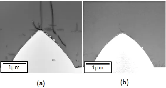
Figure 1. Sc nucle 2.3 Analysis Scanning ele (HRXRD) ar investigated b was a 400 nm power-depend excitation pho 2.4 Raman m The strain di excitation sou perform depth depth. Since local strain ca The light out
chematic diagra ation layer (sam
tools ctron microsc re used to me by measuring m laser light, dent IQE. Th oton numbers measurement istribution of urce was a 53 h-resolved Ra the phonon fr an be evaluate tput power-cur am of LED stru mple Y). The di
cope (SEM), t asure the cry power-depend
second harm he efficiency
.14
the thin film 32 nm laser l aman measure requency shift ed by analyzin rrent (L-I) ch ctures with an i iameter, space, transmission stal quality o dent photolum monically gene was defined structure wa light and the ement, the sam
t was linearly ng the Raman aracteristics o in-situ LT GaN and height of c electron micr f samples. Th minescence (P erated from a as the photo as investigated scattered ligh mple was mou proportional peak position of LEDs were nucleation laye one on PSS we roscope (TEM he optical pro L) at low and Ti-sapphire p on numbers em d by measurin ht was collecte unted on a z-ax to both the bi n. The fabricat e analyzed by er (sample X) a re 2.8, 0.2, and M), and high r operties of the room temper pulse laser (M mitted from t ng depth reso ed by a 100x xis piezo stag iaxial and uni ted LEDs had a probe statio
and an ex-situ sp d 1.8 μm, respec
resolution X-r e InGaN/GaN ature. The exc Mira 900), to the sample d olved Raman x, NA0.7 obje ge to vary the axial strain in d dimension of on and an inte puttered AlN ctively. ray diffraction N MQWs were citation source determine the divided by the spectra.15 The ective lens. To laser focusing n GaN,16, 17 the f 26 x 30 mil2 egrated sphere n e e e e e o g e 2. e
instrument un 3.1 SEM Res Figure 2 show minutes and 2 layer coverag Y with the ex formed with coverage con Figure 2. SEM (b) 20 nder CW oper sult ws the surfac 20 minutes, re ge can be obse x-situ sputtere less GaN gra ndition to enha
M top view imag minutes growth ration at room e morphology espectively. W erved on c-pla ed AlN nucle ains on the co ance c-plane re
ges of GaN epita h, and that with
temperature. 3. RESUL
y of GaN gro With the in-situ
ane spacing re eation layer (F
ne region. As egion growth
axial layer grow h an ex-situ sput
LTS AND DI
own on PSS w u LT-GaN nuc egion and the t Figure 2c and s a result, ex-and suppress
wn on PSS with ttered AlN nucl
ISCUSSION with different cleation layer top of cones. O d 2d) show th situ sputtered cone region la h an in-situ LT G leation layer aft
N
nucleation la is sample X ( On the other h hat perfect hex d AlN nucleat
ateral growth.
GaN nucleation ter (c) 10 minut
ayers for grow Figure 2a and hand, GaN lay xagonal-shape tion layer can .18, 19
n layer after (a) tes and (d) 20 m wth time of 10 d 2b), the GaN yers of sample e stack can be n offer a better 10 minutes and minutes. 0 N e e r d
3.2 TEM Result and X-ray analysis
Figure 3 shows the cross-sectional TEM image of sample X and sample Y. Some dislocations around top of pattern and air voids at cone slope area in sample X can be observed from Figure 3a. On the contrary, almost no defects and only a little air voids can be discovered around the top region of cones in sample Y. In addition, the X-ray (102) full-width at half maximum (FWHM) could be reduced from 240 of sample X to 110 arcsec of sample Y, and (002) FWHM was also from 230 to 101 arcsec. This analysis can indicates that the crystal quality of GaN layers can be effectively improved by using the ex-situ sputtered AlN nucleation layer.
Figure 3. Cross sectional TEM images of GaN epitaxial layer grown on PSS: (a) with an in-situ LT GaN nucleation layer, (b) with an ex-situ sputtered AlN nucleation layer.
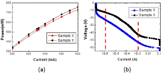
3.3 L-I curve and V-I curve
Figure 4a shows the forward bias L-I curve. The light output powers were 754 and 725 mW when the injection current was 600 mA, respectively. The light output power (LOP) of sample Y was 4.0 % higher than sample X. Figure 4b
indicates the reversed bias voltage versus reversed bias current. The reversed bias voltage of sample Y was always -10V much higher than sample X at either lower (1μA) or higher (1mA) reversed bias current, respectively. We believe that reversed bias leakage current corresponds to the dislocation density which means the better crystal quality could bring out the lower leakage current and higher reversed bias voltage.
Figure 4. (a) The forward L-I characteristics and (b) the reversed bias V-I curve of LED devices.
3.4 PL result
Figure 5a and 5b show the PL emission peak and spectra FWHM of sample X and Y as a function of excitation power at 300K, respectively. The FWHM of PL emission peak declined with the blue-shift of PL emission peak because the QCSE was gradually screened and the MQWs became flatter with increasing the carrier density at the lower excitation power. When it came to the higher excitation power, the QCSE was completely screened and the Burstein–Moss effect started to dominate the blue-shift of PL emission peak.20 At the same time, all states close to the conduction band are populated which caused large amount of carriers being pushed to higher energy states, so the FWHM of PL emission peak increased. The energy shift of PL emission peak of sample X and Y before the FWHM raising were 3.3 and 8.2 meV, respectively. The fact of that LED with the ex-situ sputtered AlN nucleation layer has higher compressive strain can be proved from the energy shift result.
3.5 Raman result
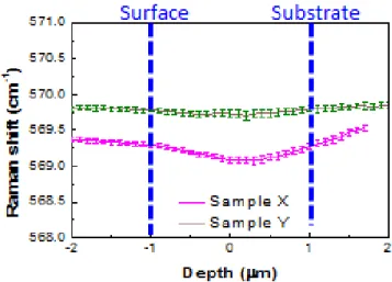
The depth resolved confocal Raman spectroscopy was analyzed to figure out strain distribution in the LED structure. Figure 6 shows the peak position of GaN E2high Raman peak from the sample surface to the substrate interface, and the
error bars was the uncertainty in the curve-fitting. The formation of defects caused partial strain release during the growth of GaN layers in sample X. Therefore, the strain around the surface was lower than that in sample Y. On the other hand, the more coherent growth of GaN layers by using the ex-situ sputtered AlN nucleation layer induced relatively high compressive strain in sample Y. Based on these analysis, we believed that better crystal quality is one of the most important factors which dominate higher light output power and reversed bias voltage although larger strain existed in LED with ex-situ sputtered AlN nucleation layer.
Figure 6. The Raman peak frequency shifts of the GaN E2
high phonon modes of sample X and Y are plotted as a function of the depth
of epitaxial layer from the p-GaN surface toward the sapphire substrate.
4. CONCLUSION
Sputtered AlN nucleation layer can reduce the dislocation formation of GaN layers and suppress crystal growth on the cone region of PSS compared with GaN layers on in-situ LT GaN nucleation layers which indicates that crystal quality of GaN layers was improved significantly by using ex-situ sputtered AlN nucleation layer. Moreover, LEDs with ex-situ sputtered AlN nucleation layers have 4.0% increase of LOP and around -10V improvement of reversed bias voltage.
Lastly, the truth was revealed by PL and depth resolved Raman measurement that LEDs with ex-situ sputtered AlN nucleation layers have larger compressive strain. However, owing to great crystal quality, LEDs with ex-situ sputtered AlN nucleation layers hold excellent performance of optical and electrical properties.
ACKNOWLEDGEMENT
The authors would like to gratefully acknowledge Crux Ou, Young Yang and Wei-Chih Wen at Epistar Corporation and Prof. S. C. Wang, and Prof. H. C. Kuo at National Chiao Tung University for technical support. This work has been supported in part by the MOE ATU program and in part by the Ministry of Science and Technology of Republic of China in Taiwan under contract numbers of NSC 102-2221-E-009-156-MY3, and MOST 104-2221-E-009-096-MY3.
REFERENCE
[1] Yoshida, S., Misawa, S. and Gonda, S., “Improvements on the electrical and luminescent properties of reactive molecular beam epitaxially grown GaN films by using AlN‐coated sapphire substrates,” Appl. Phys. Lett., 42(5), 427-429 (1983).
[2] Wu, X. H., Fini, P., Tarsa, E. J., Heying, B., Keller, S., Mishra, U. K., DenBaars, S. P. and Speck, J. S., “Dislocation generation in GaN heteroepitaxy,” J. Cryst. Growth, 189–190, 231-243 (1998).
[3] Sasaoka, C., Sunakawa, H., Kimura, A., Nido, M., Usui, A. and Sakai, A., “High-quality InGaN MQW on low-dislocation-density GaN substrate grown by hydride vapor-phase epitaxy,” J. Cryst. Growth, 189–190, 61-66 (1998). [4] Lester, S. D., Ponce, F. A., Craford, M. G. and Steigerwald, D. A., “High dislocation densities in high efficiency GaN‐based light‐emitting diodes,” Appl. Phys. Lett., 66(10), 1249-1251 (1995).
[5] Gradečak, S., Stadelmann, P., Wagner, V. and Ilegems, M., “Bending of dislocations in GaN during epitaxial lateral overgrowth,” Appl. Phys. Lett., 85(20), 4648-4650 (2004).
[6] Einfeldt, S., Roskowski, A. M., Preble, E. A. and Davis, R. F., “Strain and crystallographic tilt in uncoalesced GaN layers grown by maskless pendeoepitaxy,” Appl. Phys. Lett., 80(6), 953-955 (2002).
[7] Li, Z. Y., Lo, M. H., Hung, C.T., Chen, S.W., Lu, T. C., Kuo, H. C. and Wang, S. C., “High quality ultraviolet AlGaN/GaNAlGaN/GaN multiple quantum wells with atomic layer deposition grown AlGaN barriers,” Appl. Phys. Lett., 93(13), 131116 (2008).
[8] Hertkorn, J., Lipski, F., Brückner, P., Wunderer, T., Thapa, S. B., Scholz, F., Chuvilin, A., Kaiser, U., Beer, M., Zweck, J., “Process optimization for the effective reduction of threading dislocations in MOVPE grown GaN using in situ deposited SiNxSiNx masks,” J. Cryst. Growth, 310(23), 4867-4870 (2008).
[9] Cich, M. J., Aldaz, R. I., Chakraborty, A., David, A., Grundmann, M. J., Tyagi, A., Zhang, M., Steranka, F. M. and Krames, M. R., “Bulk GaN based violet light-emitting diodes with high efficiency at very high current density,” Appl. Phys. Lett., 101(22), 223509 (2012).
[10] Yen, C. H., Lai, W. C., Yang, Y. Y., Wang, C. K., Ko, T. K., Hon, S. J. and Chang, S. J., “GaN-Based Light-Emitting Diode With Sputtered AlN Nucleation Layer,” IEEE Photon. Technol. Lett., 24(4), 294-296 (2012).
[11] Son, J. H. and Lee, J. L., ”Strain engineering for the solution of efficiency droop in InGaN/GaN light-emitting diodes,” Opt. Express, 18(6), 5466-5471 (2010).
light-emitting diodes,” Appl. Phys. Lett., 78(18), 2617-2619 (2001).
[13] Tawfik, W. Z., Song, J., Lee, J. J., Ha, J. S., Ryu, S. W., Choi, H. S., Ryu, B. and Lee, J. K., “Effect of external tensile stress on blue InGaN/GaN multi-quantum-well light-emitting diodes,” Appl. Surf. Sci., 283, 727-731 (2013). [14] Watanabe, S., Yamada, N., Nagashima, M., Ueki, Y., Sasaki, C., Yamada, Y., Taguchi, T., Tadatomo, K., Okagawa, H. and Kudo, H., “Internal quantum efficiency of highly-efficient InxGa1−xN-based near-ultraviolet light-emitting diodes,”
Appl. Phys. Lett., 83(24), 4906-4908 (2003).
[15] Chen, W. L., Lee, Y. Y., Chang, C. Y., Huang, H. M., Lu, T. C. and Chang, Y. M., “Depth-resolved confocal micro-Raman spectroscopy for characterizing GaN-based light emitting diode structures,” Rev. Sci. Instrum., 84(11), 113108 (2013).
[16] Davydov, V. Yu., Kitaev, Yu. E., Goncharuk, I. N., Smirnov, A. N., Graul, J., Semchinova, O., Uffmann, D., Smirnov, M. B., Mirgorodsky, A. P. and Evarestov, R. A., “Phonon dispersion and Raman scattering in hexagonal GaN and AlN,” Phys. Rev. B, 58(19), 12899 (1998).
[17] Hiroshi, H., “Properties of GaN and related compounds studied by means of Raman scattering,” J. Phys.: Condens. Matter, 14(38), R967-R993 (2002).
[18] Chen, Y. C., Hsiao, F. C., Lin, B. W., Wang, B. M., Wu, Y. S. and Hsu, W. C., “The Formation and the Plane Indices of Etched Facets of Wet Etching Patterned Sapphire Substrate,” J. Electrochem. Soc., 159(6), D362-D366 (2012). [19] Lee, K. S., Kwack, H. S., Hwang, J. S., Roh, T. M., Cho, Y. H., Lee, J. H., Kim, Y. C. and Kim, C. S., “Spatial correlation between optical properties and defect formation in GaN thin films laterally overgrown on cone-shaped patterned sapphire substrates,” J. Appl. Phys., 107(10), 103506 (2010).
[20] Wu, J., Walukiewicz, W., Shan, W., Yu, K. M., Ager III, J. W., Haller, E. E., Lu, H. and Schaff, W. J., “Effects of the narrow band gap on the properties of InN,” Phys. Rev. B, 66(20), 201403(R) (2002).