國 立 交 通 大 學
電機學院光電顯示科技產業研發碩士班
碩 士 論 文
具有氟、氮離子摻雜源/汲極
低溫複晶矽薄膜電晶體之特性研究
Investigation of Low Temperature Poly-Silicon Thin
Film Transistors with Fluorine and Nitrogen
Ion implanted Source/Drain
研
究
生 : 李崇維 Chong-Wei Lee
指 導 教 授 : 劉柏村 博士 Dr. Po-Tsun Liu
低溫複晶矽薄膜電晶體之特性研究
Investigation of Low Temperature Poly-Silicon Thin
Film Transistors with Fluorine and Nitrogen
Ion implanted Source/Drain
研 究 生:李崇維 Student :
Chong-Wei Lee
指導教授:劉柏村 博士 Advisor : Dr. Po-Tsun Liu
國 立 交 通 大 學
電機學院光電顯示科技產業研發碩士班
碩 士 論 文
A Thesis
Submitted to College of Electrical Engineering and Computer Science
National Chiao Tung University
in Partial Fulfillment of the Requirements
for the Degree of
Master
in
Industrial Technology R & D Master Program on
Photonics and Display Technologies
June 2007
Hsinchu, Taiwan, Republic of China
低溫複晶矽薄膜電晶體之特性研究
研究生 : 李崇維 指導教授 : 劉柏村 博士
國立交通大學
電機學院光電顯示科技產業研發碩士班
摘要
近年來,低溫複晶矽薄膜電晶體(LTPS TFTs)相當受到矚目,這是因為低溫複晶矽薄 膜電晶體具有很高的電子移動率使然。對於液晶螢幕顯示器(LCD monitor)而言,藉此, 高 驅 動 力 的 電 路 得 以 整 合 至 玻 璃 基 板 上 , 以 實 現 系 統 電 路 在 同 一 面 板 上 (system-on-panel)。然而,對於雷射所結晶的複晶矽薄膜電晶體來說,在複晶矽晶粒邊 界處、複晶矽通道層與閘極介電層接面處存在相當多的缺陷態位密度,導致複晶矽薄膜 電晶體(Poly-Si TFTs)具有較高漏電流和較差的穩定度。除此之外,離子佈植後的退火製 程,若採用雷射退火的方式,在源/汲極與通道接面處因溫度梯度(Temperature gradient) 與繞射(Laser diffraction)緣故,產生了額外的缺陷密度(Extra-trap states),該缺 陷以"接面缺陷"(Junction defect)稱之。為了解決該接面缺陷所造成的漏電路徑,吾種類,諸如:氟(Fluorine)與氮(Nitrogen),佈植於源/汲極。該劑量均為 1x10¹⁴ 與 1x1015 cm-2 。藉由電性參數粹取方式,吾人比較對照組(不含氟與氮摻雜源/汲極)與實驗組(含氟 與氮摻雜源/汲極、劑量均為 1x1014 cm-2 )的元件,發現實驗組具有較小的次臨限擺幅 (subthreshold swings) 、 較 高 的 載 子 移 動 率 (Field mobility) 、 較 低 的 截 止 電 流 (off-state current)與較低的臨限電壓(threshold voltage)。由以上這些參數得知, 深層缺陷(deep trap state)與淺層缺陷(tail trap state)確實有被修補的效應,尤其 是接面缺陷。吾人將其歸因於,在晶粒邊界處的矽斷鍵(dangling bond),藉由氟與氮的 摻雜,晶過雷射活化後,氟、氮會與矽斷鍵形成矽-氟(Si-F)、矽-氮(Si-N)鍵結,而達 到鈍化(passivation)缺陷的目的。
Film Transistors with Fluorine and Nitrogen
Ion implanted Source/Drain
Student : Chong-Wei Lee Advisor : Dr. Po-Tsun Liu
Industrial Technology R & D Master Program of
Electrical and Computer Engineering College
National Chiao Tung University
Abstract
Low-temperature polycrystalline silicon thin film transistors (LTPS TFTs) have attracted much attention due to the possibility of realizing the integration of driving circuits and pixel elements on one substrate,and the potential to accomplish the system-on-panel(SOP)。 However large off-state leakage current and poor stability of polycrystalline silicon thin film transistors (poly-Si TFTs) fabricated by excimer laser annealing(ELA) due to high trap states in poly-Si grain boundaries and at the interface between poly-Si channel layer and gate dielectric are still serious problems。Recently it has been reported that residual ion implantation damage at source/drain junctions of ELA poly-Si TFTs entitled “junction defect” is also one of the problems of poly-Si TFTs。In order to eliminate the junction defects,we propose a poly-Si
introduced via ion implantation into the source/drain region。In addition,doses of fluorine and nitrogen varying from 1x10¹⁴ to 1x1015 cm-2 were implanted in this work。The experimental results of both F- and N-passivated(dose of 1x1014 cm-2) devices showed steeper subthreshold
swings,higher carrier mobility ,lower off-state current and lower threshold voltage than unpassivated devices。This indicates that a large fraction the defects have been passivated, junction defect especially。This is attributed to that F-、N-incorporated form Si-F and Si-N bond with silicon dangling bond at the grain boundary after laser annealing。
時光荏苒,兩年的研究所生涯在此要告一段落。憶起為學期間,有太多人讓我心存 感念。首先要感謝的是我的指導教授劉柏村老師。老師的諄諄教誨,不僅於研究上給予 諸多指導與鼓勵進而導引學生從中獲得啟發 ; 而且在待人處世方面,更是讓學生獲益良 多,因此,碩士學位才得以順利完成。此外,還要感謝中山物理研究所張鼎張教授殷勤 的指導,在此同表最誠摯的敬意及謝意。 緊接著,要感謝這兩年來在實驗過程中,學長們熱心的指教與協助,其中特別感謝 王敏全與吳興華學長在製程與實驗結果分析的教導。此外,工研院的陳宏哲學長,在準 分子雷射與拉曼分析的支援;交大材料所張志榜學長在 secco-etch 溶液的提供;中山大學 漢博在 SEM 的支援以及交大奈米中心、國家奈米實驗室的工程師與所提供的實驗機台, 在此一併表達深摯的感謝。 啟銘與唐豪,很開心這兩年有你們一路相伴與相挺,不論是感情上或實驗上,在我 人生最低潮的時候,適時给予關懷與協助,這份革命情感我畢生永難忘懷。當然還要感 謝逸哲、建文、昇翰學長們、子怡學姐、柏宇同學、誼明與逸侑學弟,有了你們,讓我 的生活著實多了一份精采。同時,感謝一德、弘根、千睿學長、秀娟、宛芳、建民、志 晟、任偉、立夫、亞諭、原園…等等諸事幫忙。 此外,我要感謝我最要好的六位死黨金鋒、汶鴻、瑋修、崇訓、詩偉和信賢,在我 感情最薄弱的時候有所慰藉,在此,將這份喜悅與你們共享。 最後,由衷的感謝我最敬愛的父母及親愛的弟弟。你們一直是我精神上最大的支柱, 讓我能無後顧之憂的致力於研究工作,終使學業得以順利完成。筆末,謹以此論文獻給 所有關心我的家人與朋友。 李崇維 2007.06
Chinese Abstract
……….IEnglish Abstract
………...……….III
Chinese Acknowledgements
………..…………...…………...V
Contents
………...……..………..VI
Table Captions…...VIII
Figure Captions... IX
Chapter 1 Introduction
1.1 General Background……….……….…...……11.1.1 Overview of Poly-Silicon thin-film transistors……….………1
1.1.2 Defects in Poly-Si film……….……….3
1.1.3 Transport properties of Poly-Si……….………4
1.1.4 Non-ideal effect……….………8
1.2 Motivation....………...……….………..9
1.3 Thesis Organization……….………...10
Chapter 2 Fabrication and Experiment
2.1 Device Structure and Fabrication...132.2 Electrical Characteristics Measurement...17
2.3 Device Parameter Extraction...17
2.3.1 Determination of threshold voltage………..………17
2.3.2 Determination of subthreshold swing………...………18
2.3.3 Determination of field effect mobility………..…19
Chapter 3 Result and Discussion
3.1 Electrical Analysis……….………….23
3.1.1 Device characteristic of ELA poly-silicon TFTs with fluorine incorporation…...23
3.1.2 Device characteristic of ELA poly-silicon TFTs with nitrogen incorporation...27
3.1.3 Comparison between ELA poly-Silicon TFTs with fluorine and nitrogen implantation………..29
3.2 Material Analysis………...30
3.2.1 Scanning electron microscopy(SEM)………30
3.2.2 Sheet resistance of laser activation………31
Chapter 4 Conclusion...
....55Chapter2
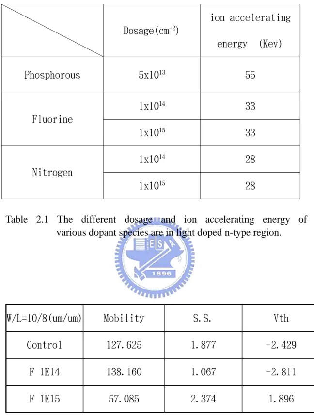
Table 2.1 The different dosage and ion accelerating energy of various dopant
species are in light doped n-type region.
Chapter3
Table 3.1 Key parameters of poly-Si TFTs with different fluorine dosage.
Table 3.2 The relation between the electrical parameter and the location of the
trap states.
Table 3.3 Transfer Line method parameters of poly-Si TFTs with different
fluorine implantation dosage.
Table 3.4 Key parameters of poly-Si TFTs with different nitrogen dosage.
Table 3.5 Transfer Line method parameters of poly-Si TFTs with different
nitrogen implantation dosage.
Table 3.6 Key parameters of poly-Si TFTs with fluorine and nitrogen ion
implantated.
Table 3.7 The different dosage and ion accelerating energy of various dopant
species are in heavy doped n-type region.
Chapter1
Fig.1-1 Sketch of the band diagram of the polycrystalline silicon films.
Fig.1-2 A schematic MOSFET cross section, showing the axes of coordinates
and the bias voltages at the four terminals for the drain-current model.
Fig.1-3 Three possible mechanisms of leakage current in poly-Si TFTs,
including thermionic emission, thermionic field emission and pure
tunneling
Fig.1-4 The kink effect in the output characteristics of an n-channel SOI
MOSFET
Fig.1-5 Rresidual ion implantation damage at source/drain junctions of
ELA poly-Si TFTs entitled “junction defect”
Chapter2
Fig.2-1 The top view of TFT
Fig.2-2 Cross-section view of TFT
Fig.2-3 Schematic of transfer line method from source to drain resistance.
Chapter3
Fig.3-1 Transfer characteristic for fluorine implanted ELA Poly-Si TFT and
control ELA Poly-Si TFT at V
D=0.1V
control ELA Poly-Si TFT at V
D=5V
Fig.3-3 Field effect mobility (μ
FE) as a function of the different fluorine
implantation dosage ELA poly-Si TFTs.
Fig.3-4 Threshold voltage (V
th) as a function of the different fluorine
implantation dosage ELA poly-Si TFTs.
Fig.3-5 Subthreshold Swing (S.S.) as a function of the different fluorine
implantation dosage ELA poly-Si TFTs.
Fig.3-6 Output characteristic for fluorine implanted ELA Poly-Si TFT and
control ELA Poly-Si TFT
Fig.3-7 Parasitic resistance (Rp) as a function of the different fluorine
implantation dosage ELA poly-Si TFTs.
Fig.3-8 Effective Mobility (μ
eff) as a function of the different fluorine
implantation dosage ELA poly-Si TFTs.
Fig.3-9 Si
I+-P
+pairs enhance the the growth of extrinsic defects
Fig.3-10 Transfer characteristic for nitrogen implanted ELA Poly-Si TFT and
control ELA Poly-Si TFT at V
D=0.1V
Fig.3-11 Transfer characteristic for nitrogen implanted ELA Poly-Si TFT and
control ELA Poly-Si TFT at V
D=5V
implantation dosage ELA poly-Si TFTs.
Fig.3-13 Threshold voltage (V
th) as a function of the different nitrogen
implantation dosage ELA poly-Si TFTs.
Fig.3-14 Subthreshold Swing (S.S.) as a function of the different ditrogen
implantation dosage ELA poly-Si TFTs.
Fig.3-15 Output characteristic for nitrogen implanted ELA Poly-Si TFT and
control ELA Poly-Si TFT
Fig.3-16 Parasitic resistance (Rp) as a function of the different nitrogen
implantation dosage ELA poly-Si TFTs.
Fig.3-17 Effective Mobility (μ
eff) as a function of the different nitrogen
implantation dosage ELA poly-Si TFTs.
Fig.3-18 Transfer characteristic for fluorine and nitrogen implanted ELA
Poly-Si TFT and control ELA Poly-Si TFT at V
D=0.1V
Fig.3-19 Transfer characteristic for fluorine and nitrogen implanted ELA
Poly-Si TFT and control ELA Poly-Si TFT at V
D=5V
Fig.3-20 The activation energy of drain current as a function of gate voltage
measured at VD=5V for standard, fluorine and nitrogen ion implanted
ELA poly-Si TFTs
measured at VD=5V for standard, fluorine and nitrogen ion implanted
ELA poly-Si TFTs
Fig.3-22 SEM image of ELA-processed poly-Si film after secco-etch
Fig.3.23 The schematic cross section view of devices
Fig.3.24 Sheet resistance(Rs) as a function of the laser energy density for
different fluorine ion implanted dosage.
Fig.3.25 Sheet resistance(Rs) as a function of the laser energy density for
different nitrogen ion implanted dosage.
Chapter 1
Introduction
1.1 General Background
1.1.1 Overview of Poly-Silicon thin-film transistors
In recent years, polycrystalline silicon thin-film transistors (poly-Si TFTs) have drawn
much attention because of their widely applications on active matrix liquid crystal displays
(AMLCDs) [1], and organic light-emitting displays (OLEDs) [2]. Except large area displays,
poly-Si TFTs also have been applied into some memory devices such as dynamic random
access memories (DRAMs) [3], static random access memories (SRAMs) [4], electrical
programming read only memories (EPROM) [5], electrical erasable programming read only
memories (EEPROMs) [6], linear image sensors [7], thermal printer heads [8], photo-detector
amplifier [9], scanner [10], neutral networks [10]. Lately, some superior performances of
poly-Si TFTs also have been reported by scaling down device dimension or utilizing novel
crystallization technologies to enhance poly-Si film quality [11-12]. This provides the
opportunity of using poly-Si TFTs into three-dimension (3-D) integrated circuit fabrication.
Of course, the application in AMLCDs is the primary trend, leading to rapid developing of
poly-Si TFT technology. The major attraction of applying polycrystalline silicon thin-film
elements and the capability to integrate panel array and peripheral driving circuit on the same
substrates [13-15]. In poly-Si film, carrier mobility larger than 15 cm2/Vs can be easily
achieved, that is enough to used as peripheral driving circuit including n- and p-channel
devices. This enables the fabrication of peripheral circuit and TFT array on the same glass
substrate, bring the era of system-on-glass (SOG) technology. The process complexity can be
greatly simplified to lower the cost. In addition, the mobility of poly-Si TFTs is much better
than that of amorphous ones, the dimension of the poly-Si TFTs can be made smaller compared to that of amorphous Si TFTs for high density、high resolution AMLCDs, and the
aperture ratio in TFT array can be significantly improved by using poly-Si TFTs as pixel
switching elements. This is because that the device channel width can be scaled down while
meeting the same pixel driving requirements as in α-Si TFT AMLCDs. For making high
performance poly-crystalline silicon (poly-Si) thin film transistors (TFTs) [16],
low-temperature technology is required for the realization of commercial flat-panel displays
(FPD) on inexpensive glass substrate, since the maximum process temperature is limited to less than 600℃. There three major low-temperature amorphous-Si crystallization methods to
achieve high performance poly-Si thin film, solid phase crystallization (SPC), excimer laser
crystallization (ELC), and Metal-Induced Lateral Crystallization (MILC) However, some
problems still exist in applying poly-Si TFTs on large-area displays. In comparison with
defects, and the electrical activity of the charge-trapping centers profoundly affects the
electrical characteristics of poly-Si TFTs. Large amount of defects serving as trap states locate
in the disordered grain boundary regions to degrade the ON current seriously [17]. Moreover,
the relatively large leakage current is one of the most important issues of conventional poly-Si
TFTs under OFF-state operation [18-19]. In most application, a low-cost substrate is essential and therefore a low temperature process (i.e., <650°C) compatible with glass 2 substrates is
developed [20]. In summary, it is expected that the poly-Si TFTs will becomes more
important in future technologies, especially when the 3-D circuit integration era is coming.
More researches studying the related new technologies and the underlying mechanisms in
poly-Si devices with shrinking dimensions are therefore worthy to be indulged in.
1.1.2 Defects in Poly-Si film
Due to the granular structure of the poly-Si film, a lot of grain boundaries and intragranular
defects exist in the film. The dangling bonds in grain boundaries will affect device
characteristics seriously because they act as trapping centers to trap carriers. Carriers trapped
by these low energy traps can no longer contribute to conduction, which results in the
formation of local depletion region and potential barriers in these grain boundaries. Thus, the
typical characteristics such as threshold voltage, subthreshold swing, ON current, mobility
and transconductance of TFTs are inferior to those of devices fabricated on single crystal
the drain voltage and gate voltage. The dominant mechanism of the leakage current is field
emission via grain boundary traps due to the high electric field near the drain junction [21-24].
To overcome this inherent disadvantage of poly-Si film, many researches have been focused
on modifying or eliminating these grain boundary traps. Traps are associated with dangling
bonds arising from lattice discontinuities between different oriented grains or at the Si/SiO2
interface. The most useful method so far to remove traps is to passivate these dangling bonds,
such as hydrogen plasma treatment has been utilized for the passivation [25-26], but it is
difficult to control the hydrogen concentration in the TFT. The Si-H bonds may be broken
under hot-carrier stress [27-28], leading to degradation of electrical characteristics after a
long-term operation time. As the number of trapped carrier decreases, the potential barriers in
grain boundaries decrease. And the leakage current decreases because of the fewer trap
density near the drain region.
1.1.3 Transport properties of Poly-Si
As mentioned in section 1.1.1 and 1.1.2, the device characteristics of poly-Si TFTs are
strongly influenced by the grain structure in poly-Si film. Even though the inversion channel
region is also induced by the gate voltage as in MOSFETs, the existence of grain structure in
channel layer bring large differences in carrier transport phenomenon. Many researches
studying the electrical properties and the carrier transport in poly-Si TFTs have been reported.
[29-31]. In this model, it is assumed that the poly-Si material is composed of a linear chain of
identical crystallite having a grain size Lg and the grain boundary trap density Nt. The charge
trapped at grain boundaries is compensated by oppositely charged depletion regions
surrounding the grain boundaries. It is shown in Figure. 1-1. From Poisson’s equation, the
charge in the depletion regions causes curvature in the energy bands, leading to potential
barriers that impede the movement of any remaining free carriers from one grain to another.
When the dopant/carrier density n is small, the poly-Si grains will be fully depleted. The
width of the grain boundary depletion region xd extends to be Lg/2 on each side of the
boundary, and the barrier height VB can be expressed as
s g d s B qnL x qn V ε ε 8 2 2 2 = = (1-1)
As the dopant/carrier concentration is increased, more carriers are trapped at the grain
boundary. The curvature of the energy band and the height of potential barrier increase,
making carrier transport form one grain to another more difficult. When the dopant/carrier
density increases to exceed a critical value N* = Nt / Lg, the poly-Si grains turn to be partially
depleted and excess free carriers start to spear inside the grain region. The depletion width
and the barrier height can be expressed as
n N x t d 2 = (1-2) n qN n N qn V s t t s B ε ε 8 ) 2 ( 2 2 2 = = (1-3)
The depletion width and the barrier height turn to decrease with increasing dopant/carrier
density, leading to improved conductivity in carrier transport. The carrier transport in fully
depleted poly-Si film can be described by the thermionic emission over the barrier. Its’
current density can be written as [32]. )] ( exp[ V V KT q qnv J = c − B − (1-4)
where n is the free-carrier density, vc is the collection velocity ( v = kT m∗ c / 2π ), VB is the
barrier height without applied bias, and Vg is the applied bias across the grain 8
boundary region. For small applied biases, the applied voltage divided approximately
uniformly between the two sides of a grain boundary. Therefore, the barrier in the
forward-bias direction decreases by an amount of Vg/2. In the reserve-bias direction, the
barrier increases by the same amount. The current density in these two directions then can be
expressed as )] 2 1 ( exp[ B g c F V V KT q qnv J = − − (1-5) )] 2 1 ( exp[ B g c F V V KT q qnv J = − + (1-6)
the net current density is then given by
) 2 sinh( ) exp( 2 KT qV KT qV qnv J B g c − = (1-7)
at low applied voltages, the voltage drop across a grain boundary is small compared to the
thermal voltage kT/q, Eq. (1.7) then can be simplified as
)] exp( 2 ) exp( 2 2 KT qV KT V nv q KT qV KT qV qnv J B g c g B c − = − = (1-8)
the average conductivity σ = J / Ε = JLg / Vg and the effective mobility μeff = σ / qn
then can be obtained
) exp( 2 KT qV KT L nv q B g c − = σ (1-9) ) exp( ) exp( KT qV KT qV KT L qnv B o B g c eff = − ≡μ − μ (1-10)
where μ0 represents the carrier mobility inside grain regions. It is found that the conduction
in poly-Si is an activated process with activation energy of approximately qVB, which depends
on the dopant/carrier concentration and the grain boundary trap density. Applying gradual
channel approximation to poly-Si TFTs, which assumes that the variation of the electric field
in the y-direction (along the channel) is much less than the corresponding variation in the
z-direction (perpendicular to the channel), as shown Fig. 1-2. The carrier density n per unit
area (cm-2) induced by the gate voltage can be expressed as
ch y TH G ox qt V V V C n= ( − − ( )) (1-11) dy dv V V V C W dy dV nqdx dz dxdy dy dv nq Jdxdy I y t y TH G ox eff y eff W y eff D ch
∫
∫
∫ ∫
∫ ∫
− − = = = = 0 ) ( 0 μ μ ( ) μ (1-12)where tch is the thickness of the inversion layer. Therefore, the drain current ID of poly-Si TFT
then can be given by
(
)
∫
L=
⎢⎣
⎡
−
−
⎥⎦
⎤
0 22
1
D D th g ox eff Ddy
W
C
V
V
V
V
I
μ
(
)
⎥⎦⎤ ⎢⎣ ⎡ − − = 2 2 1 D D th g ox eff D C V V V V L W I μ (1-13)Obviously, this I-V characteristic is very similar to that in MOSFETs, except that the mobility
is modified.
1.1.4 Non-ideal effect
There are two major non-ideal effects will limit the TFTs application, including leakage
current and kink-effect. The mechanism of these two non-ideal effects is described briefly as
bellow.
1.1.4.1. Leakage current
In AMLCD, TFTs play a switching device to turn ON/OFF the current path for
charging/discharging the liquid crystal capacitor. Thus, the leakage current should be low
enough to remain a pixel gray level before it must be refreshed. The leakage current
mechanism in poly-Si has been studied by Olasupe [33]. The leakage current resulted from
carrier generation from the poly-Si grain boundary defects. There are three major leakage
mechanisms, as shown in Fig. 1-3. The dominant mechanism is a function of the prevailing
drain bias. They pointed out carrier generation from grain boundary defects via thermionic
emission and thermionic field emission to be prevalent at a low and medium drain biases, and
carrier pure tunneling from poly-Si grain boundary defects to be the dominant mechanism at
higher drain bias.
1.1.4.2. Kink effect[34]
Majority carriers, holes in the p-substrate for an n-channel poly-Si TFTs, generated by impact
ionization will be stored in the substrate, since there is no substrate contact to drain away
these charges. Therefore the substrate potential will be changed and will result in a reduction
of the threshold voltage. This, in turn, may cause an increase or a kink in the current-voltage
characteristics. The kink phenomenon is shown in Fig. 1-4. This float-body or kink effect is
especially dramatic for n-channel devices, because of the higher impact-ionization rate of
electrons. The kink effect can be eliminated by forming a substrate contact to the source of the
transistor.
1-2. Motivation
Low-temperature polycrystalline silicon thin film transistors (LTPS TFTs) have attracted
much attention due to the possibility of realizing the integration of driving circuits and pixel elements on one substrate,and the potential to accomplish the system-on-panel(SOP)。To
meet the requirement of higher circuit density and higher speed, it is necessary to improve the
performance of the poly-Si TFTs. However, it has been shown that the performances of
poly-Si are affected by the trap states at grain boundaries. In the preview research, Enlarging
the grain size and passivating the defects at the grain boundary were widely used methods to
reduce the trap states in the grain boundary. Generally, hydrogen plasma treatment has been
utilized for the passivation, but it is difficult to control the hydrogen concentration in the
electrical characteristics by eliminating the defects in the grain boundary [35-37].However
large off-state leakage current and poor stability of polycrystalline silicon thin film transistors
(poly-Si TFTs) fabricated by excimer laser annealing(ELA) due to high trap states in poly-Si
grain boundaries and at the interface between poly-Si channel layer and gate dielectric are still serious problems。Recently it has been reported that residual ion implantation damage at
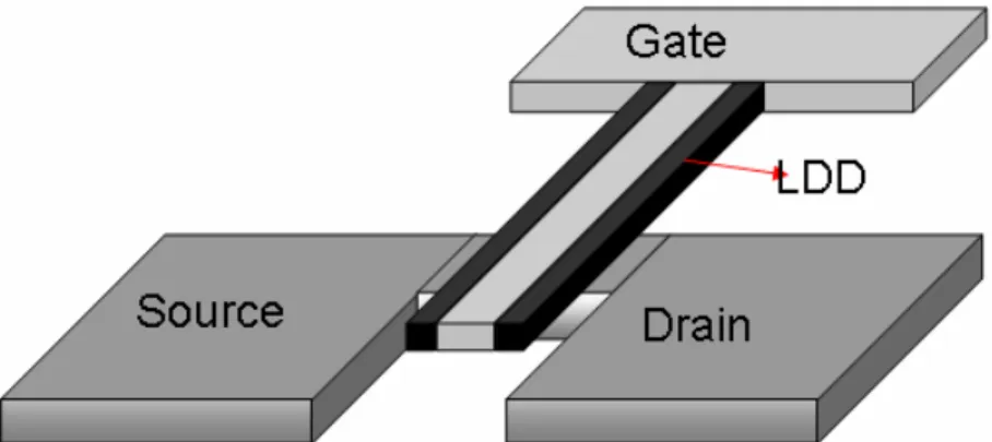
source/drain junctions of ELA poly-Si TFTs entitled “junction defect” shown in Fig. 1-5 [38]is also one of the problems of poly-Si TFTs。In order to eliminate the junction defects,
we propose a poly-Si defect passivation technique wherein the passivating species (Fluorine and Nitrogen) is introduced via ion implantation into the source/drain region。In addition,
doses of fluorine and nitrogen varying from 1x10¹⁴ to 1x1015 cm-2 were implanted in this work。The electrical characteristics, including I-V measurement , were reported in this study.
1.3 Thesis Organization
Chapter 1 Introduction
1.1 General Background
1.1.1 Overview of Poly-Silicon thin-film transistors
1.1.2 Defects in Poly-Si film
1.1.3 Transport properties of Poly-Si
1.2 Motivation
1.3 Thesis Organization
Chapter 2 Fabrication and Experiment
2.1 Device Structure and Fabrication2.2 Electrical Characteristics Measurement
2.3 Device Parameter Extraction
2.3.1 Determination of threshold voltage
2.3.2 Determination of subthreshold swing
2.3.3 Determination of field effect mobility
2.3.4 Determination of parasitic resistance
2.3.5 Determination of activation energy
Chapter 3 Result and Discussion
3.1 Electrical Analysis3.1.1 Device characteristic of ELA poly-silicon TFTs with fluorine incorporation
3.1.2 Device characteristic of ELA poly-silicon TFTs with nitrogen incorporation
3.1.3 Comparison between ELA poly-Silicon TFTs with fluorine and nitrogen
3.2 Material Analysis
3.2.1 Scanning electron microscopy(SEM)
3.2.2 Sheet resistance of laser activation
Chapter 2
Fabrication and Experiment
2.1 Device Structure and Fabrication
It has been reported that the lightly-doped-drain (LDD) structure can effectively decrease the leakage current and the kink current in polysilicon TFTs due to reduction of the electric field intensity near the drain region. However, the above device fabrication processes need more intensive or complex process integration. In this thesis, the poly-Si TFTs with various Fluorine and Nitrogen ion implantation doses were proposed and fabricated. The top view of the devices and the schematic cross section view of devices were shown in Fig. 2.1 and Fig 2.2 , respectively. The fabrication procedure is described as following.
step1
. Substrate.6-inch 100-mm-thick p-type single-crystal silicon wafers with (100) orientation were used as the starting materials. After a standard cleaning procedure, silicon wafers were coated with 500-nm-thick thermally grown SiO2 in steam oxygen ambient at 1000ºC. In order to
simulate the thin film transistor environment, the thick thermal oxide was grown on Si wafers.
step2
.Buffer Oxide Layer.layer of deposited SiO2 prior to the deposition of poly-Si. In this work, wafers were deposited
with 1μm-thick thermally grown wet oxide (SiO2) in steam oxygen and hydrogen ambient at
970℃ by high temperature system.
step3
Poly-Si film formation.We deposited 500-nm α-Si films by LPCVD system.The α-Si films were performed using silane(SiH4) as a reactant gas at 550℃.In this study, poly-Si film re-crystallized
methods used were the continuous scanning for large area crystallization(Excimer Laser Anneal, ELA).During laser 308nm XeCl excimer laser with a beam spot of 1.8 x 23.1mm2 was irradiated with scanned with 98% overlap from pulse to pulse with the repetition rate 20Hz for continuous scanning. The laser energy density was 320mJ/cm2.After lithography and transformer couple plasma (TCP9400-SE) etching (in steam mixed Cl2 and HBr ambient at 65℃ by 7mTorr), the devices active region were form.
Step4. Gate oxide formation.
After defining the active region, the photoresist was removed by using O3 plasma etching
and pure H2SO4 solution. The following step was to remove the polymer which was formed
during the plasma etching. The remove for residue of polymer was realized by SC1 solution (NH4OH:H2O2:H2O=0.25:1:5). Before gate oxide deposition, the STD clean was used to clean
the wafers. The HF dip was necessary to remove the native oxide at the poly-Si surface. Then, a 50nm layer of tetra-ethyl-ortho-silicate (TEOS) gate oxide was deposited by LPCVD at 700 ℃. The thickness of gate oxide was determined by N&K optical analyzer.
Step5. Gate electrode formation.
After deposition of gate insulators, 300-nm-thick poly-silicon films were formed immediately on the gate insulators by LPCVD at 620℃. There was no any chemical solution clean between the deposition of TEOS oxide and poly-Si gate. The second poly-Si layer was then patterned by transformer couple plasma (TCP9400-SE) etching to define the gate regions.
Step6. Light-doped-drain regions formation.
After the gate definition, source and drain regions were formed by phosphorous and Fluorine or Nitrogen ions implantation. The ion accelerating energy and the dosage are show in Table 2.1.
Step7. Spacer formation.
A 400nm-thick SiO2 oxide, used as spacer layer, was deposited at 350℃ by HDP-CVD system.After deposition, the spacer profile were patterned by reactive ion etching system (TEL5000S) with 5.8nm/sec of etching rate.
Step8.Heavy-doped n-type regions formation
After the spacer definition, heavy-doped n-type regions were formed by phosphorous ions implantation. The ion accelerating energy is at 60 KeV and the dosage is 1x1015 cm-2. Step9.Post-implantation anneal
Post-implantation annealing methods were used to active the implanted dopants. Based on above, we choose the laser annealing method. During laser irradiation, the 308nm XeCl excimer laser with scanned with 95% overlap from pulse to pulse for continuous scanning. The laser energy density was 250mJ/cm2.
Step10. Passivation layer and contact hole formation.
The passivation layer was used by HDP-CVD of low temperature system. The passivation layer was 500-nm-thick to cap the poly-Si TFTs devices. Then the contact holes were patterned and etched by buffer oxide etching (BOE) solution. The size of contact holes were 5x5 μm2.
Step11. Metallization.
The 700-nm aluminum layers were deposited by physical vapor deposition (PVD) and then patterned at the source, drain, and gate electrode as the metal pads.
2.2 Electrical Characteristics Measurement
The electrical property analysis instrument mainly used the Agilent 4156A semiconductor analyzer. The Agilent 4156A semiconductor analyzer with probe stations was used to analyze the electrical properties of the devices. In our experiment, it was used for I-V measurement and bias-temperature-stress (BTS). The ground probe station was provided an electrical isolation. The water-cooled thermal plate within an optical shielding box and plate could be controlled by the TPO315A thermal controller between 25°C and 300°C. The source measurement units (SMUs) were used to control voltage sources where current flowing through could be measured. The voltage or current sources were supplied by Agilent 4156A semiconductor analyzer.
2.3 Device Parameter Extraction
In this section, we will introduce the methods of typical parameters extraction such as threshold voltage (VTH), subthreshold slope (S.S), field-effect mobility (μFE), parasitic
resistance(Rp), and activation energy (Ea) .
2.3.1 Determination of threshold voltage
Many methods are used to determinate the threshold voltage (VTH) which is the most
determinate the threshold voltage is constant drain current method where the gate voltage at a specified drain current IN value is taken as the threshold voltage. This technique is adopted in
most studies of TFTs. Typically, the threshold current IN = ID / (Weff / Leff ) is specified at 10
nA for VD = 0.1V (linear region) and 100 nA for VD = 5V (saturation region) in most papers to
extract the threshold voltage of poly-Si TFTs.
2.3.2 Determination of subthreshold swing
Subthreshold swing (V/dec.) is a typical parameter to describe the gate control ability of gate toward channel. It is defined as the amount of gate voltage required to increase/decrease drain current by one order of magnitude. The subthreshold swing should be independent of drain voltage and gate voltage. However, in reality, subthreshold swing might increase with drain voltage due to short-channel effects such as charge sharing, avalanche multiplication, and punchthrough-like effect. The subthreshold swing is also related to gate voltage due to undesirable factors such as serial resistance and interface state.
The subthreshold swing of the transfer characteristics is defined as ) log( . . D G I V S S Δ Δ =
In this experiment, the subthreshold swing is defined as the gate voltage required to decrease the threshold current by one orders of magnitude (from 10-9A to 10-7A).
2.3.3 Determination of field effect mobility
The field-effect mobility (μFE) is determined from the transconductance (gm) at low drain
voltage (VD=0.1V). The transfer I-V characteristics of poly-Si TFT can be expressed as
(
)
⎥⎦⎤ ⎢⎣ ⎡ − − = 2 2 1 D D TH G ox FE D V V V V L W C I μ whereCox is the gate oxide capacitance per unit area,
W is channel width, L is channel length,
VTH is the threshold voltage.
If VD is much smaller than VG-VTH ( i.e. VD << VG-VTH ) and VG > VTH, the drain current can be
approximated as:
(
G TH)
D ox FE D V V V L W C I =μ −The transconductance is defined as
D FE ox const V G D m L V WC V I g D μ = ∂ ∂ = | = .
Therefore, the field-effect mobility can be obtained by
m D ox FE C WV g L = μ
Besides of photo leakage current, we also carry about the ON current of device. As the TFT-LCD display is larger, we have shorter time to charge the storage capacitor to certain voltage. So improving ON current is the main solution to charge capacitor in short time. We propose a solution to solve the ON current issue by using a low resistance channel to replace the a-Si:H channel. According to the Transfer Line Method (TLM model), seeing figure 2-3 , it shows that the resistance between source and drain are channel resistance and two parasitic resistance[39] . parastic channel on R R R = +2 where:
(
G T)
channel V V C W L R − = 1 1 μand:Rparastic is independent of L L:channel length
W: channel width
m : mobility
VG: gate voltage
VT: threshold voltage
Because poly film have less resistance than a-Si:H film, we choose direct deposited poly film to replace the conventional a-Si:H film and we reduce the channel resistance[40]. We also use direct deposited N+ poly to reduce parasitic resistance too .As long as the total resistance can be lowered, the mobility can be raised. Therefore, the on current can be increased too.
2.3.5 Determination of activation energy
When gate voltage is applied in field effect structures, positive gate voltages cause accumulation of electrons near the gate/channel interface. The induced electrons fill the available states above the Fermi level. Then, the Fermi level is shifted towards the conduction band EC (towards higher energy). Negative gate voltages cause emission of electrons from the
states below the Fermi level. Consecutively, Fermi level shift towards the valence band EV
(towards lower energy levels).
The rate at which EF moves towards the conduction band (in n-channel poly-Si TFTs) depends
on the density of states located in the band gap and on the distribution of tail states close to the conduction band. When gate voltage (Vg) is small, the Fermi level is located in deep states.
Increasing Vg leads to a shift of the Fermi level towards the conduction band, and the tail band
states become important. Other way to shift the Fermi level is by thermal activation of the carriers. IDS in poly-Si TFTs can be temperature activated [41]. From measurements of the
temperature dependent current at constant gate voltage (Vg), we can deduce the activation
energy Ea= EC-EFas a function of the gate voltage. To use the following dependence:
⎟⎟ ⎠ ⎞ ⎜⎜ ⎝ ⎛ − × − = − 1 2 1 2 1 1 ln ln T T K E B a σ σ DS DS V I d W L 1 1 = × × σ DS DS V I d W L 2 2 = × × σ Where
1
σ is channel conductivity at temperature T1,
2
σ is channel conductivity at temperature T2,
I DS1 is the drain-source current at temperature T1,
I DS 2 is the drain-source current at temperature T2,
K B is the Boltzmann constant,
W is the length of the channel, L is the width of the channel, d is the thickness of the channel.
By measuring the drain-source voltage at different temperatures and keeping the same drain-source current, and then the activation energy (i.e. the Fermi level position) can be determined from the slope of the Arrhenius plot (log(IDS) vs. 1000/T) by the following
equation: ⎟⎟ ⎠ ⎞ ⎜⎜ ⎝ ⎛ − × × × − = − 1 2 1 2 1000 1000 ) log( 1000 log log T T K e E I I B a DS DS
If we apply different gate voltages (Vg), we will get different channel conductivity and
corresponding drain-source current. Therefore, different Arrhenius plots can be obtained for each value of Vg. The activation energy can be found as a function of the gate voltage. For
Chapter 3
Result and Discussion
3.1 Electrical Analysis
3.1.1 Device characteristic of ELA poly-silicon TFTs with fluorine incorporation
Fig. 3.1 and Fig. 3.2 show typical transfer characteristics for various fluorine ion implantation dosages and standard poly-Si TFTs at VD=0.1V and VD=5V, respectively.
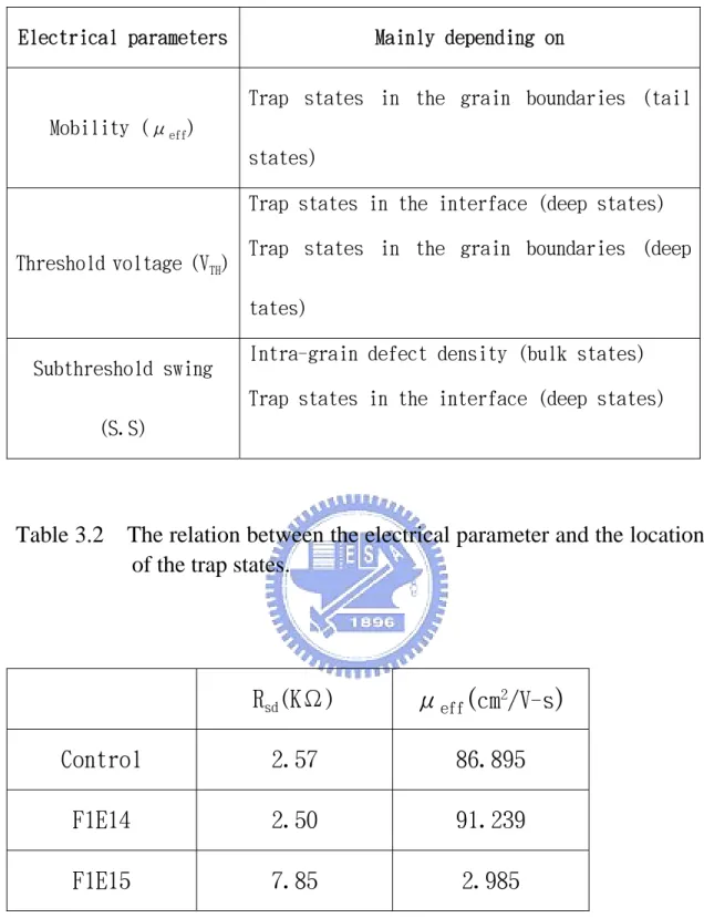
Table 3.1 lists key parameters of poly-Si TFTs. Fig. 3-3 to 3-5 show the TFTs’ field effect mobility (μFE), threshold voltage (VTH), subthreshold swing (S.S) as a function of various
fluorine ion implantation dosage, respectively. This result showed that the electrical characteristics could be improved for the fluorine ion implantation dosage was at 1x1014cm-2. The field effect mobility increased from 127.625 to 138.160 cm2/V-s. The increasing μFE,
decreasing VTH and steep S.S make it more potential for poly-Si TFTs application. As the
implantation dosage increased to 1x1015cm-2, the electrical characteristics had a serious degradation compared with 1x1014cm-2 implanted devices. It was found that the over amount
of fluorine ion implantation doses caused the degraded electrical characteristics. The mechanism will be discussed in the following sections.
The output characteristics of the fluorine implanted poly-Si TFTs and control TFTs are compared as shown in Fig. 3-6. It was found that the TFT with 1x1014cm-2implantation doses
had the highest drain current in the same drain voltage, and drain current had degradation when the implantation dosage increased to 1x1015cm-2implantation doses. This trend is the same as the transfer characteristics as shown in Fig. 3-1 and Fig. 3-2.
3.1.1.1 The effects of fluorine passvation.
It was known that the electrical characteristics of poly-Si TFTs, such as field effect mobility (μFE), threshold voltage (VTH), and subthreshold swing (S.S), were affected by the
trap state density [42-44]. Table 3.2 lists their relationship. From above relation, we can know the increasing effect mobility, steep subthreshold swing and the decreasing threshold voltage compared with control without fluorine incorporation are attributed to tail states and deep states had been repaired for the TFTs with 1x1014cm-2implantation doses. Moreover, it is reported that the fluorine atoms in the poly-Si channel can also passivate the dangling bonds to decrease deep state density [45], resulted in the subthreshold swing of the implanted device were improved. Because of that, we infer that fluorine atoms diffuse from source/drain region to channel and pile up at the SiO2/poly-Si interface. By the fluorine incorporation, fluorine
atoms bond with dangling Si and Si-O bonds so that the trap states had been terminated. Furthermore, fluorine atoms can break the stress induced strained bonds, likely the strained Si-O-Si bonds and Si-Si bonds to form stronger Si-F bonds, leading to local stress relaxation and thus decreasing the tail state density. In order to realize whether fluorine diffuse from source/drain region to channel or not, the transfer line method [39] such as below have been
used.
Transfer Line Method:
m
R :total serious resistance
ch
R :channel resistance
SD
R :Source/Drain resistance L :physical channel length
L
Δ :dopants diffusion length
eff
L
:typical channel length
eff
μ :effective intrinsic carrier mobility eff
W
:effective channel width
From above formula, we measure the output characteristics of poly-Si TFTs with different channel length, and extract the parameters such as RSDand μeff shown in Table 3.3
and Fig. 3.7 to Fig. 3.8
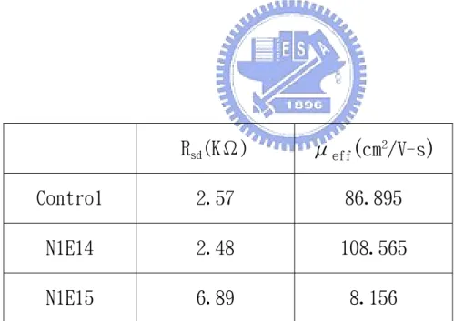
As shown in Table 3.3 , effective intrinsic carrier mobility is 91.239(cm2/V-s) for the fluorine device with implantation dosage of 1x1014cm-2 , that is, the fluorine atoms diffusing from source/drain region to channel region lead to trap states had been repaired. Therefore, during the post-implantation annealing, the junction defects located in the junction between channel and source/drain region were eliminated by diffusing fluorine atoms. In addition, interface states were also passivated, resulted in the subthreshold swing of the implanted device were improved. Source/Drain resistance is 2.50 (KΩ) for the fluorine device with implantation dosage of 1x1014cm-2.The lower Source/Drain resistance result from trap density terminated leads to the higher on-state current.
The other phenomenon was observed in the Fig. 3.1 , TFTs’ field effect mobility (μFE),
threshold voltage (VTH), subthreshold swing (S.S) and drain current had degradation when the
implantation dosage increased to 1x1015cm-2 implantation doses. It is reported that new fluorine ion implantation technique reduces the growth of extrinsic defects, and dopant activation, on the contrast, enhances the sheet resistance in high-dose phosphorous(P) ion-implanted layers [46]. The supersatuation of SiI(interstitial silicon atoms) in high-dose
phosphorous ion-implanted layers and they conclude that SiI trapping may occur through
some kind of bond between P and SiI during the ion implantation. During post-implantation
an additional fluorine (F) ion implantation was carried out, F atoms seemed to be trapped easily by P dopants rather than SiI and created F--P+ pairs, due to the high electronegativity of
F atoms, and possibly the strength of the electronic bond. F--P+ pairs reduce the dopant activation, and prevent phosphorous dopants from creating electronically trapped SiI during
ion implantation and post-implantation anneal. As a result, growth of the extrinsic defects are reduced by appropriate fluorine dosage. On the contrary, over dosage leads to F--P+ pairs is too much due to the high electronegativity of F atoms and generates extrinsic defects . F--P+ pairs reduce the carrier concentration result from Si-P pairs lost to cause the increasing parasitic resistance. Moreover, extrinsic defects degrade the electrical characteristics of poly-Si TFTs.
3.1.2 Device characteristic of ELA poly-silicon TFTs with nitrogen incorporation
Fig. 3.10 and Fig. 3.11 show typical transfer characteristics for various nitrogen ion implantation dosages and standard poly-Si TFTs at VD=0.1V and VD=5V, respectively.
Table 3.4 lists key parameters of poly-Si TFTs. Fig. 3-12 to 3-14 show the TFTs’ field effect mobility (μFE), threshold voltage (VTH), subthreshold swing (S.S) as a function of various
nitrogen ion implantation dosage, respectively. This result showed that the electrical characteristics could be improved for the nitrogen ion implantation dosage was at 1x1014cm-2. The field effect mobility increased from 127.625 to 155.310 cm2/V-s. The increasing μFE,
decreasing VTH and steep S.S make it more potential for poly-Si TFTs application. As the
implantation dosage increased to 1x1015cm-2, the electrical characteristics had a serious degradation compared with 1x1014cm-2 implanted devices. It was found that the over amount
of nitrogen ion implantation doses caused the degraded electrical characteristics. The mechanism will be discussed in the following sections.
The output characteristics of the nitrogen implanted poly-Si TFTs and control TFTs are compared as shown in Fig. 3-15. It was found that the TFT with 1x1014cm-2implantation doses had the highest drain current in the same drain voltage, and drain current had degradation when the implantation dosage increased to 1x1015cm-2implantation doses. This trend is the same as the transfer characteristics as shown in Fig. 3-10 and Fig. 3-11.
3.1.2.1 The effects of nitrogen passvation.
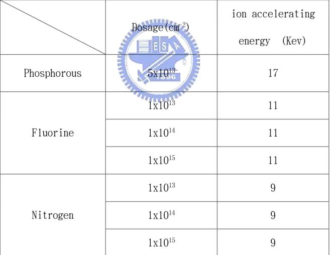
As shown in Table3.4, we can know the increasing effect mobility, steep subthreshold swing and the decreasing threshold voltage compared with control without nitrogen incorporation are attributed to tail states and deep states had been repaired for the TFTs with 1x1014 cm-2 implantation doses. Moreover, it is reported that the nitrogen-implanted polysilicon TFT had the better performance [47-48]. Base on above reasons , the improved electrical characteristics might be attributed to nitrogen atoms diffusing from source/drain region to channel region. By the nitrogen incorporation, nitrogen atoms bond with dangling Si and Si-O bonds so that the trap states had been terminated. In order to obtain the source/drain resistance , the transfer line method [39] have been used. The results are shown in Table3.5
and Fig. 3.16 to Fig. 3.17. The value of the source/drain resistance reflects the on-state current of poly-Si TFTs. The lower the source/drain resistance is , the higher the on-state current is. This indicates that nitrogen itself has some passivation effect on trap states of source/drain region for the TFTs with 1x1014cm-2implantation doses. Source/Drain resistance increased when the implantation dosage increased to 1x1015cm-2implantation doses. The nitrogen atoms whould increase the source/drain resistance due to the increasing electron scattering probably, which will result in the decrease of the drain current.
The other phenomenon was observed in the Fig. 3.10 , TFTs’ field effect mobility (μFE),
threshold voltage (VTH), subthreshold swing (S.S) and drain current had degradation when the
implantation dosage increased to 1x1015cm-2 implantation doses. The over amount of nitrogen ion implantation doses result in lots of Si-N bonds in the poly-Si film. The more Si-N bonds ,the lower conductivity in the nitrogen implanted poly-Si film.
3.1.3 Comparison between ELA poly-Silicon TFTs with fluorine and nitrogen
Fig. 3.18 and Fig. 3.19 show typical transfer characteristics for various fluorine and nitrogen ion implantation dosages and standard poly-Si TFTs at VD=0.1V and VD=5V,
respectively. Table 3.6 lists key parameters of poly-Si TFTs. Significantly, we can see that N passivation results in the highest mobility and the steepest subthreshold slope, followed by F passivation. It is likely that the passivation reaction is limited by kinetics as the silicon film cools within 1 μs after excimer laser pulse [49]. The efficacy of passivation correlates well
with the bonding enthalpies between Si and the passivation species: Si-N has the lowest enthalpy(470 kJ/mol), so that Si-N bonds are formed most easily, followed by Si-F(553 kJ/mol).[50]
3.1.3.1 The activation energy variation with fluorine and nitrogen incorporation
Fig. 3-20 shows the activation energy of drain current as a function of gate voltage measured at VD=5V for standard , nitrogen and fluorine ion implanted poly-Si TFTs. the
activation energy was extracted by the measurement of ID-VG characteristic in the temperature
range from 30°C to 90°C. It was found that the activation energy was reduced for fluorine and nitrogen ions implanted poly-Si TFTs when the devices turn on. It implied that the trap density eliminate by using fluorine and nitrogen ions implantation. However, In the off state we found that the activation energy of the fluorine and nitrogen ions implanted TFTs was higher than that of the standard TFTs, resulted from lower leakage current as shown in Fig. 3-18. When the implantation dosage increased to 1x1015cm-2 implantation doses, the activation energy as shown in Fig. 3.21 was increased for fluorine and nitrogen ions implanted poly-Si TFTs when the devices turn on. It indicated that trap density increased on the contrary.
3.2 Material Analysis
3.2.1 Scanning electron microscopy(SEM)
approximately 250nm.
3.2.2 Sheet resistance of laser activation
In this work, the poly-Si film with various Fluorine and Nitrogen ion implantation doses were proposed and fabricated. The schematic cross section view of devices were shown in Fig. 3.23. The fabrication procedure is described as following.
4-inch 100-mm-thick p-type single-crystal silicon wafers with (100) orientation were used as the starting materials. To prevent impurity diffusion from the substrate, the substrate is general covered with a layer of deposited SiO2 prior to the deposition of poly-Si. In this
work, wafers were deposited with 1μm-thick thermally grown wet oxide (SiO2) in steam
oxygen and hydrogen ambient at 970℃ by high temperature system. We deposited 500-nm α-Si films by LPCVD system. The α-Si films were performed using silane(SiH4) as a reactant
gas at 550℃.In this study, poly-Si film re-crystallized methods used were the continuous scanning for large area crystallization(Excimer Laser Anneal, ELA).During laser 308nm XeCl excimer laser with a beam spot of 1.8 x 23.1mm2 was irradiated with scanned with 98% overlap from pulse to pulse with the repetition rate 20Hz for continuous scanning. The laser energy density was 320mJ/cm2. Following recrystallization, phosphorous and Fluorine or Nitrogen ions implantation were performed. The ion accelerating energy and the dosage are show in Table 3.7. Post-implantation annealing methods were used to active the implanted dopants. Based on above, we choose the laser annealing method. During laser irradiation, the
308nm XeCl excimer laser with scanned with 95% overlap from pulse to pulse for continuous scanning. The laser energy density were 100, 200, 250, 300mJ/cm2. Finally, sheet resistances were measured using four-point probe method.
Fig.3-24. shows that sheet resistance (Rs) as a function of the laser energy density for different fluorine ion implanted dosage samples. Fig.3-25. shows that sheet resistance(Rs) as a function of the laser energy density for different nitrogen ion implanted dosage samples. As shown in Fig 3-24. and Fig. 3-25., when the laser energy density was below 250 mJ/cm2, the damage owing to ion-implantation didn’t repaired completely. With the increasing laser energy density, sheet resistance decreased. Sheet resistance gets up to optimum value until laser energy density is 250 mJ/cm2. Moreover, while the laser energy density is 250 mJ/cm2, sheet resistance of experimental devices with additional fluorine ions incorporation of 1x10¹³ or 1x1014cm-2doses is lower than that of control devices. It means that passivation effect occurs. By the fluorine incorporation, the trap density has been terminated. The phenomenon is also observed in the nitrogen case. Sheet resistance increased when the implantation dosage increased to 1x1015cm-2implantation doses. The causes had been discussed in section 3.1.1.1 and 3.1.2.1.
energy (Kev)
Phosphorous
5x10
1355
1x10
1433
Fluorine
1x10
1533
1x10
1428
Nitrogen
1x10
1528
Table 2.1 The different dosage and ion accelerating energy of
various dopant species are in light doped n-type region.
W/L=10/8(um/um)
Mobility
S.S.
Vth
Control
127.625
1.877
-2.429
F 1E14
138.160
1.067
-2.811
F 1E15
57.085
2.374
1.896
Mobility (μeff)
Trap states in the grain boundaries (tail states)
Threshold voltage (VTH)
Trap states in the interface (deep states) Trap states in the grain boundaries (deep tates)
Subthreshold swing (S.S)
Intra-grain defect density (bulk states) Trap states in the interface (deep states)
Table 3.2 The relation between the electrical parameter and the location
of the trap states.
R
sd(KΩ)
μ
eff(
cm
2/V-s
)
Control
2.57
86.895
F1E14
2.50
91.239
F1E15
7.85
2.985
Table 3.3 Transfer Line method parameters of poly-Si TFTs with
different fluorine implantation dosage.
W/L=10/8(um/um)
Mobility
S.S.
Vth
Control
127.625
1.877
-2.429
N 1E14
155.310
0.907
-5.333
N 1E15
63.540
2.270
-0.536
Table 3.4 Key parameters of poly-Si TFTs with different nitrogen dosage.
R
sd(KΩ)
μ
eff(
cm
2/V-s
)
Control
2.57
86.895
N1E14
2.48
108.565
N1E15
6.89
8.156
Table 3.5 Transfer Line method parameters of poly-Si TFTs with
different nitrogen implantation dosage.
Control
127.625
1.877
-2.429
F 1E14
138.160
1.067
-2.811
N 1E14
155.310
0.907
-5.333
Table 3.6 Key parameters of poly-Si TFTs with fluorine and nitrogen
ion implantated.
Dosage(cm
-2)
ion accelerating
energy (Kev)
Phosphorous
5x10
1317
1x10
1311
1x10
1411
Fluorine
1x10
1511
1x10
139
1x10
149
Nitrogen
1x10
159
Table 3.7 The different dosage and ion accelerating energy of
various dopant species are in heavy doped n-type region.
Fig.1-1 Sketch of the band diagram of the polycrystalline
silicon films
Fig.1-2 A schematic MOSFET cross section, showing the axes of
coordinates and the bias voltages at the four terminals for the
drain-current model.
Fig.1-3 Three possible mechanisms of leakage current in poly-Si TFTs,
including thermionic emission, thermionic field emission and
pure tunneling
Fig.1-4 The kink effect in the output characteristics of an n-channel SOI
MOSFET
Fig.1-5 Rresidual ion implantation damage at source/drain junctions of
ELA poly-Si TFTs entitled “junction defect”
Fig.2-1 The top view of TFT
Fig. 2-2 Cross-section view of TFT
Rchannel Rparasitic Rparasitic D S channel on R R R = + /
Fig.2-3 Schematic of transfer line method from source to drain
resistance.
Fig.3-1 Transfer characteristic for fluorine implanted ELA Poly-Si TFT
and control ELA Poly-Si TFT at V
D=0.1V
Fig.3-2 Transfer characteristic for fluorine implanted ELA Poly-Si TFT
and control ELA Poly-Si TFT at V
D=5V
Fig.3-3 Field effect mobility (μ
FE) as a function of the different fluorine
implantation dosage ELA poly-Si TFTs.
Fig.3-4 Threshold voltage (V
th) as a function of the different fluorine
Fig.3-5 Subthreshold Swing (S.S.) as a function of the different fluorine
implantation dosage ELA poly-Si TFTs.
Fig.3-6 Output
characteristic for fluorine implanted ELA Poly-Si TFT
and control ELA Poly-Si TFT
Fig.3-7 Parasitic resistance (Rp) as a function of the different fluorine
implantation dosage ELA poly-Si TFTs.
Fig.3-8 Effective Mobility (μ
eff) as a function of the different fluorine
interstitial Si atom
:Phosphorous atom
SiI- -P+ pairs reduce the dopant activation
n+ region
Fig.3-9 Si
I+-P
+pairs enhance the the growth of extrinsic defects
Fig.3-10 Transfer characteristic for nitrogen implanted ELA Poly-Si
TFT and control ELA Poly-Si TFT at V
D=0.1V
Fig.3-11 Transfer characteristic for nitrogen implanted ELA Poly-Si
TFT and control ELA Poly-Si TFT at V
D=5V
Fig.3-12 Field effect mobility (μ
FE) as a function of the different
Fig.3-13 Threshold voltage (V
th) as a function of the different nitrogen
implantation dosage ELA poly-Si TFTs.
Fig.3-14 Subthreshold Swing (S.S.) as a function of the different
ditrogen implantation dosage ELA poly-Si TFTs.
Fig.3-15 Output
characteristic for nitrogen implanted ELA Poly-Si TFT
and control ELA Poly-Si TFT
Fig.3-16 Parasitic resistance (Rp) as a function of the different nitrogen
implantation dosage ELA poly-Si TFTs.
Fig.3-17 Effective Mobility (
μ
eff) as a function of the different nitrogen
ELA Poly-Si TFT and control ELA Poly-Si TFT at V
D=0.1V
Fig.3-19 Transfer characteristic for fluorine and nitrogen implanted
ELA Poly-Si TFT and control ELA Poly-Si TFT at V
D=5V
voltage measured at VD=5V for standard, fluorine and
nitrogen ion implanted ELA poly-Si TFTs
Fig.3-21 The activation energy of drain current as a function of gate
voltage measured at VD=5V for standard, fluorine and
nitrogen ion implanted ELA poly-Si TFTs
Fig.3-22 SEM image of ELA-processed poly-Si film after secco-etch
Fig.3.24 Sheet resistance(Rs) as a function of the laser energy density
for different fluorine ion implanted dosage.
Fig.3.25 Sheet resistance(Rs) as a function of the laser energy density
for different nitrogen ion implanted dosage.
Chapter 4
Conclusion
Low temperature poly-silicon thin film transistors with fluorine and nitrogen ion
implanted source/drain were investigated in this study. In order to eliminate the junction
defects, we propose a poly-Si defect passivation technique wherein the passivating species
(Fluorine and Nitrogen) is introduced via ion implantation into the source/drain region.
Without plasma treatment , Source/Drain with fluorine and nitrogen ion-implanted dosage of
1x1014 cm-2 Poly-Si TFTs have already achieved better device performances, such as a higher mobility, a lower threshold voltage and a steeper subthreshold swing. It is believed that the
fluorine and nitrogen atoms diffusing from source/drain region can break the stress induced
strained bonds, likely the strained Si-O-Si bonds and Si-Si bonds to form stronger Si-F bonds,
leading to local stress relaxation and thus decreasing the tail state density. Moreover, the
fluorine and nitrogen atoms in the poly-Si channel can also passivate the dangling bonds to
decrease deep state density. In addition, the lower off-state current indicates that “Junction
defect” owing to laser beam diffraction had been repaired. The higher on-state current implied
that activation efficiency in source/drain region improved. Source/Drain with fluorine and
nitrogen ion-implanted dosage of 1x1015 cm-2 Poly-Si TFTs lead to poor device performances. Higher source/drain resistance results from F--P+ pairs for fluorine passivation and electron scattering for nitrogen passivation.