行政院國家科學委員會專題研究計畫 成果報告
前瞻矽奈米元件變異性及傳輸特性綜合研究(II)
研究成果報告(精簡版)
計 畫 類 別 : 個別型 計 畫 編 號 : NSC 99-2221-E-009-174- 執 行 期 間 : 99 年 08 月 01 日至 100 年 07 月 31 日 執 行 單 位 : 國立交通大學電子工程學系及電子研究所 計 畫 主 持 人 : 蘇彬 計畫參與人員: 碩士班研究生-兼任助理人員:余昌鴻 碩士班研究生-兼任助理人員:江俊賢 碩士班研究生-兼任助理人員:周劭衡 博士班研究生-兼任助理人員:吳育昇 博士班研究生-兼任助理人員:郭俊延 博士班研究生-兼任助理人員:胡璧合 報 告 附 件 : 出席國際會議研究心得報告及發表論文 處 理 方 式 : 本計畫可公開查詢中 華 民 國 100 年 10 月 30 日
前瞻矽奈米元件變異性及傳輸特性綜合研究(II)
計畫編號 : NSC 99-2221-E-009-174
執行期限 : 99 年 08 月 01 日 至 100 年 07 月 31 日
主持人 : 蘇彬
國立交通大學電子工程學系
一、中文摘要 本計畫針對前瞻矽基奈米元件的變異 性及載子傳輸特性,進行綜合研究。在工 作 項 目 一 中 , 我 們 探 討 使 用 應 變 矽 (strained silicon)對奈米元件隨機匹配 之溫度相依性的影響。這項研究不僅對使 用先進 CMOS 製程的電路設計很重要,也有 助於對矽奈米元件本質參數變異的深入了 解。在工作項目二中,我們藉由載子遷移 率之超低溫量測與分析,探討應變對矽元 件 表 面 粗 糙 散 射 遷 移 率 (surface-roughness limited mobility)的影響。這 項研究有助於了解應變矽元件的戴子傳輸 機制,並對提升戴子遷移率的元件設計提 供洞見。在工作項目三中,著眼於未來可 使用鍺作為通道材料以進一步提升元件效 能,並採用超薄層(ultra-thin body)結構 改善鍺元件的靜電特性,本研究發展解析 理論模型,用以探討並比較量子侷限效應 對於極微縮超薄層鍺及矽通道元件的通道 長度變異敏感度的影響。我們的元件模型 也將有助於未來超薄層電晶體的設計。 關鍵詞 : 應 變 矽 , 超 薄 層 電 晶 體 , 量 子 侷 限 , 匹 配,變異性,表面粗糙散射遷移率 AbstractThis project conducts a comprehensive study of variability and carrier transport for advanced silicon-based nanodevices. In task I, we investigate the impact of uniaxial strain on the temperature dependence of mismatching properties of nanoscale MOSFETs. This study is important not only for circuit designs using advanced strained-silicon technologies, but also for the fundamental understanding of intrinsic parameter fluctuations in CMOS
devices. In task II, we provide an experimental assessment of surface-roughness limited mobility under uniaxial strain through cryogenic temperature measurements. This study has facilitated the understanding of carrier transport in strained-silicon, and provided insights in device designs for future mobility scaling. In task III, we report the impact of quantum confinement on the short-channel effect (SCE) and threshold-voltage sensitivity to channel-length variation for ultra-thin-body (UTB) GeOI and SOI MOSFETs using a derived analytical solution of Schrödinger equation. Our theoretical study indicates that, due to the discrepancy in effective mass, the impact of quantum confinement must be considered when one-to-one comparisons between UTB GeOI and SOI MOSFETs regarding the SCE are made.
Keywords :
Strained silicon, ultra-thin-body transistor, quantum confinement, mismatch, variability, surface-roughness limited mobility
二、計畫目的及研究方法
This project aimed to conduct a comprehensive study of variability and carrier transport for advanced silicon-based nanodevices [1]. This report details the following three major tasks carried out during the project:
Task I: Temperature dependence of drain
current mismatch in nanoscale uniaxial-strained MOSFETs [2]
Task II: Experimental investigation of
surface-roughness limited mobility in uniaxial strained MOSFETs [3]
Task III: Impact of quantum confinement on the threshold-voltage roll-off of ultra-thin-body GeOI and SOI MOSFETs [4]
Task I
Device mismatch and its temperature dependence are becoming increasingly important because they may limit the achievable accuracy in analog applications and mixed-mode integrated circuits [5]-[7]. Regarding the temperature dependence of MOSFET mismatching properties, Andricciola
et al. [6] have shown that as temperature
decreases, both the threshold voltage mismatch (Vth) and the normalized current
factor mismatch (σ(Δβ)/β) increase. In addition, Mennillo et al. [7] have suggested that the enhanced current factor mismatch as temperature decreases can be attributed to the increased Coulombic scattering. As strained-silicon is widely used in state-of-the-art CMOS technologies [8]-[10], however, the impact of strain on the temperature dependence of mismatching properties for nanoscale transistors is rarely known and merits investigation.
In this work, we examine the drain current mismatch of uniaxially-strained pMOSFETs under various temperatures and report our findings on the intrinsic effect of uniaxial strain.
Task II
Strain technology has been considered as a key process knob for advanced CMOS technologies [11]. It is known that strain can improve phonon-scattering limited mobility (PH) by reducing intervalley phonon
scatterings and effective conduction mass [12]. Whether strain can improve the surface-roughness limited mobility (SR) is still not
clear and demands more experimental investigations. Recently, the biaxial strain dependence of SR has been examined by
Bonno et al. [13] and Zhao et al. [14]. These studies have shown that SR has strong strain
sensitivity for both NFETs and PFETs due to surface morphology engineering with biaxial strain. The temperature dependences of hole mobility by mechanical uniaxial strain [15]
and process-induced uniaxial strain [16] have also been studied experimentally. However, the temperature range was higher than 87 K, and the phonon scattering mechanism was not fully suppressed. To investigate the uniaxial strain dependence of surface roughness mobility, it is necessary to extract mobility with temperature down to 20 K to suppress the phonon scattering mechanism.
In this work, we report our new findings on the impact of process-induced uniaxial strain on the SR of short-channel pMOSFETs
with temperature down to 20 K.
Task III
Germanium as a channel material has been proposed to enable the mobility scaling for CMOS devices. As the higher permittivity makes Ge more susceptible to short-channel effects (SCEs), ultra-thin-body (UTB) Ge-on-Insulator (GeOI) structure with thin buried oxide (BOX) has been suggested to improve the electrostatic integrity [17][18]. With the scaling of channel thickness, the quantum-confinement effect may become significant and impact the SCE of scaled UTB devices. Using density gradient model [19], Omura et
al. [20] have observed increased threshold
voltage (Vth) roll-off due to quantum confinement in UTB Si-on-insulator (SOI) devices. Whether there exists any difference between GeOI and SOI devices regarding the impact of quantum confinement on SCEs is not clearly known and merits investigation.
In this work, we tackle the problem using an analytically derived solution of Schrödinger equation verified with TCAD simulation. We report our new findings for UTB GeOI MOSFETs with thin BOX. The theoretical model provides us a physical and efficient method to explore the impact of quantum-confinement effect.
三、結果與討論
1. Temperature Dependence of Drain Current Mismatch in Nanoscale Uniaxial-Strained MOSFETs [2]
This work investigates the drain current mismatch of uniaxially-strained pMOSFETs under various temperatures. Fig. 1 shows the Pelgrom plot of Vth under various
temperatures for the strained and unstrained devices. The geometries of the devices are
W/Lgate=1μm/54nm, 0.3μm/54nm, and
0.15μm/54nm. Note that the Lgate for strained
devices needs to be the same in order to keep similar strain in the channel because the channel strain is gate-length dependent in process-induced strain silicon devices [10]. The linear relationship between σΔVth and
(WLgate)-1/2 indicates a
random-dopant-fluctuations origin Vth [24]. In addition, the
strained device shows similar temperature dependence of σΔVth as compared with its
control counterpart. Since the σ(ΔId)/Id in the
low |Vgst| regime is mainly determined by the
σΔVth [22], the similar temperature
dependence of σΔVth results in similar
temperature dependence of σ(ΔId)/Id for the
strained and unstrained devices as shown in Fig. 2.
In the high |Vgst| regime, however, the
strained device shows different temperature dependence of σ(ΔId)/Id as compared with its
control counterpart. It can be seen from Fig. 3 that in the high |Vgst| linear regime the σ(ΔId)/Id
increases with decreasing temperature for both the strained and unstrained devices. The temperature dependence of σ(ΔId)/Id in Fig. 3
can be explained by the temperature dependence of σ(Δβ)/β, as shown in Fig. 4. The increased σ(Δβ)/β with decreasing temperature has been attributed to the Coulombic scattering [6][7]. However, it should be noted that the σ(ΔId)/Id of the
strained device in Fig. 3 exhibits smaller temperature dependence than that of the unstrained one. The smaller temperature
dependence of σ(ΔId)/Id for strained devices
results from the smaller temperature dependence in σ(Δβ)/β (Fig. 4). It is the significantly enhanced β for the strained device as temperature decreases that reduces the temperature sensitivity of σ(Δβ)/β and σ(ΔId)/Id for the strained device. The larger
temperature sensitivity of β present in the compressively-strained PFET results from the larger temperature sensitivity of carrier mobility, as reported in [16].
Fig. 5 compares the temperature dependence of σ(ΔId)/Id for the strained and
unstrained devices in the high |Vgst| saturation
regime. It can be seen that the temperature dependence of σ(ΔId)/Id for the strained device
is opposite to that of the unstrained one. In other words, the compressive strain has changed the temperature trend in drain current mismatch and the σ(ΔId)/Id decreases with
temperature for the strained PFET. In the high
|Vgst| saturation regime, both the threshold
voltage mismatch and current factor mismatch are relevant to the σ(ΔId)/Id [22]. The
decreased σ(ΔId)/Id for the strained device
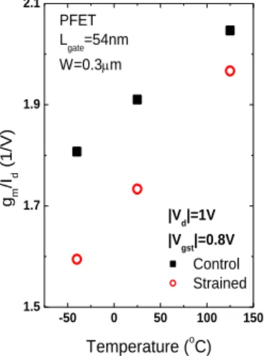
results from the larger reduction in gm/Id
reduction as temperature decreases (Fig. 6), while the σ(ΔId)/Id of the unstrained device is
weakly dependent on temperature because of the opposite temperature dependence of σΔVth
(Fig. 1) and gm/Id (Fig. 6). The larger reduction
in gm/Id as temperature decreases for the
strained device is also a consequence of the larger temperature sensitivity of carrier mobility [16].
In summary, we have investigated and analyzed the device mismatching properties of nanoscale uniaxial strained pMOSFETs under various temperatures. Our result indicates that the drain current mismatch versus temperature trend for the strained device is different from the unstrained one. In the high |Vgst| linear
regime, the compressively-strained device shows smaller increment in drain current mismatch than the unstrained counterpart as temperature decreases. In the high |Vgst|
saturation region, opposite to the unstrained case, the drain current mismatch of the compressively-strained device decreases with temperature. The underlying mechanism is the larger temperature sensitivity of carrier mobility for the strained device.
2. Experimental Investigation of Surface-Roughness Limited Mobility in Uniaxial Strained MOSFETs [3]
This work investigates the impact of process-induced uniaxial strain on the surface-roughness limited mobility, SR, of
short-channel pMOSFETs. Fig. 7 shows the measured carrier mobility versus vertical electric field (EEFF) with various temperatures.
It can be seen that, under high EEFF, the
mobility tends to increase as the temperature decreases due to suppressed phonon scattering. At a temperature lower than 60 K, the mobility at high EEFF saturates because the phonon
scattering mechanism is fully suppressed. In other words, the mobility at high EEFF within
this temperature range can be viewed as the surface-roughness limited mobility.
Fig. 8 shows the extracted carrier mobility versus temperature at EEFF = 1.6
MV/cm for various stressors. It can be seen that the compressive uniaxial strain results in a significant mobility enhancement due to band engineering and carrier repopulations [10]. In addition, SR dominates the total mobility for
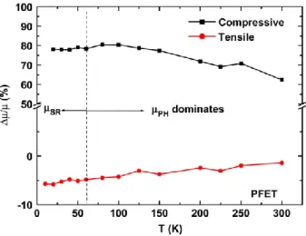
temperature < 60 K for all kinds of stressors. Fig. 9 shows the mobility enhancement percentage (Δ/) versus temperature with compressive and tensile stressors. As the temperature decreases, it can be observed that the mobility enhancement increases and saturates at temperature < 60 K where surface roughness scattering dominates. It indicates that SR has stronger stress sensitivity than the phonon-scattering limited mobility, PH.
Furthermore, the SR enhancement tends to saturate and shows little sensitivity to temperature.
It is worth noting that our experimental results are consistent with the reported results by simulations [15][25][26]. Specifically, it was reported in [25] that the scattering rate with interfacial roughness can be reduced by smoother interfaces in biaxial strained NFETs. In addition, the atomic scale model in [26] also indicated weaker surface scattering potential in strained Si due to the nature of primitive defects. For the uniaxially strained PFET case, it is plausible that the lighter effective conduction mass [5] induced by compressive strain may result in the SR enhancement.
Fig. 10 shows the extracted carrier mobility versus effective vertical electric field (EEFF) for neutral and compressive stressors at
20 K. Within this temperature range, both the Coulomb scattering and surface roughness scattering mechanisms are crucial in the determination of the overall carrier mobility. It can be seen that the mobility is dominated by the surface roughness scattering mechanism for EEFF higher than 1.2 MV/cm. The inset of
Fig. 10 shows that the SR enhancement
increases with EEFF in the high-EEFF regime
where the carrier mobility is dominated by surface roughness scatterings.
In summary, by accurate split C–V mobility extraction, the strain dependence of
SR in short-channel pMOSFETs has been
investigated under cryogenic temperatures. Our measured data indicate that SR can be
significantly enhanced by the uniaxial compressive strain. Furthermore, the SR has
higher strain dependence than the PH. Our
experimental results confirm the previously reported results based on simulations.
3. Impact of Quantum Confinement on the Threshold-Voltage Roll-Off of Ultra-Thin-Body GeOI and SOI MOSFETs [4]
This work investigates the impact of quantum confinement on the short-channel effect (SCE) and threshold-voltage sensitivity to channel-length variation for ultra-thin-body (UTB) GeOI and SOI MOSFETs using a
derived analytical solution of Schrödinger equation. Note that for long-channel undoped UTB devices, the conduction band edge EC(x)
was usually treated as a triangular well [27]. However, to account for the source/drain coupling due to SCEs, the conduction band edge EC(x) should be treated as a parabolic
well [28] with potential energy EC(x) = x2 + x + where , , and are channel-length-dependent coefficients and can be obtained from the channel potential solution of Poisson’s equation under subthreshold region [29]. Using the parabolic-well treatment, the wavefunction can be expressed as Ψj(x) =
dnxn where the coefficients dn’s can be
determined by the recursive relationship [4]. The jth eigen-energy Ej can be
determined by the boundary condition Ψj(x=0)
= Ψj(x=Tch) = 0 where x=0 and x=Tch (channel thickness) are defined as the interface positions of BOX/channel and channel/gate oxide, respectively. Thus, the eigen-energy and eigenfunction of short-channel UTB MOSFETs under subthreshold region can be derived. We have verified our model using the TCAD simulation that numerically solves the self-consistent solution of 2-D Poisson and 1-D Schrödinger equations [30]. Fig. 11(a) and (b) show that for both the triangular potential well of long-channel devices and the parabolic well (due to SCEs) of short-channel ones, the
Ej’s calculated by our model are fairly accurate.
Note that a scalable quantum-confinement (QC) model with accurate channel length dependence is crucial to this work.
Using the calculated eigen-energies and wavefunctions, the electron density can be derived [4]. Fig. 12 shows that the peak of electron density calculated by the classical (CL) model is not located at the channel/BOX interface (x=0) because the use of thin BOX (10nm) instead of thick BOX suppresses the buried-insulator induced barrier lowering (BIIBL) [20]. Although the peak of electron density calculated by the QC model is shifted toward the channel center, the main current
flow paths predicted by both models are quite similar for the UTB structure with thin BOX.
To assess the impact of quantum confinement on Vth, the Vth is defined as the VGS at which the average electron density of the cross-section at y = Leff/2 (highest potential barrier for low VDS) exceeds the channel doping concentration. Fig. 13 shows that for GeOI MOSFETs with channel thickness (Tch) = 10nm, the Vth roll-off (defined as Vth(L)– Vth(L=100nm)) predicted by the QC model is larger than that predicted by the CL model. This is consistent with the result reported for SOI MOSFET [20], and can be explained as follows. The Vth shift due to the QC effect can be expressed as VthQM S/(ln10kT/q)sQM with S being the subthreshold swing and
sQM being the equivalent surface potential shift due to the QC effect. The inset of Fig. 13 shows that for GeOI devices with larger Tch (10nm), the ―electrical confinement‖ [27] dominates the carrier quantization. The E0 (ground-state eigen-energy) of the triangular well (for long-channel devices) is much larger than that of the parabolic well (for short-channel devices) because of the larger electric field in the triangular one. As sQM is mainly determined by E0, the sQM and thus VthQM for the long-channel device is larger than that of the short-channel one. Therefore, the Vth roll-off considering the QC effect is larger in Fig. 13.
As the Tch scales down, however, a different trend can be observed. Fig. 14 shows that for GeOI MOSFETs with Tch = 5nm, the Vth roll-off predicted by the QC model becomes smaller than that predicted by the CL model, which is opposite to the larger Tch case. This can not be explained by the reduction of BIIBL due to the QC effect [20] because in this study, thin BOX (TBOX = 10nm) is used and the impact of BIIBL is not significant (see Fig. 12). Since the ―structural confinement‖ [27] dominates the carrier quantization for GeOI devices with smaller Tch (5nm), the inset of Fig. 14 shows that the E0 (and hence sQM)
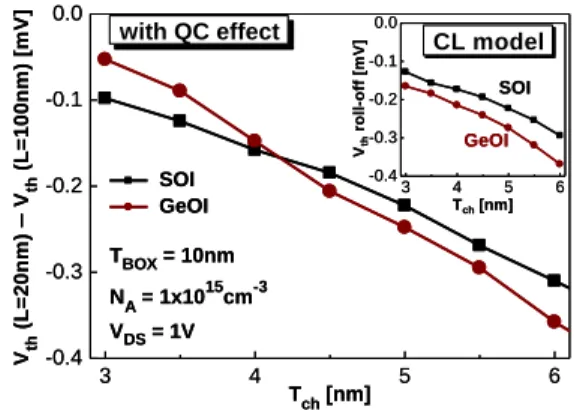
of the long-channel device is close to that of the short-channel one. Nevertheless, due to the SCE, the subthreshold swing S of the short-channel device is larger than the long-short-channel one. Therefore, the VthQM of the short-channel device is larger than that of the long-channel device and the Vth roll-off considering the QC effect is smaller. This mechanism is important because it may alter the comparison result for Vth roll-off between SOI and GeOI devices. Fig. 15 shows that, contrary to the prediction by the CL model, the Vth roll-off for GeOI devices with smaller Tch can be smaller than that of the SOI counterparts as the QC effect is considered.
In summary, depending on Tch, the quantum-confinement effect may increase or decrease the SCE of UTB devices. The critical channel thickness (Tch,crit) determining whether the QC effect increases or decreases the Vth roll-off depends on the BOX thickness (TBOX) and the channel material. Fig. 16 shows that the Tch,crit of GeOI MOSFETs increases with TBOX. In addition, for a given TBOX, the Tch,crit of SOI MOSFETs is smaller than that of the GeOI MOSFETs. This may explain why the suppression of Vth roll-off by the QC effect was not observed for the UTB SOI devices (with Tch = 10nm) in [20].
四、計畫成果自評
In this project we have conducted a comprehensive study of variability and carrier transport for advanced silicon-based devices. We have investigated the impact of uniaxial strain on the temperature dependence of mismatching properties of nanoscale MOSFETs. This study is important not only for circuit designs using advanced strained-silicon technologies, but also for the fundamental understanding of intrinsic parameter fluctuations in CMOS devices. In addition, we have experimentally examined the impact of uniaxial strain on the surface-roughness limited mobility using cryogenic temperature measurements. This study has
facilitated the understanding of carrier transport in strained-silicon, and provided insights in device designs for future mobility scaling. Besides, we have investigated the impact of quantum confinement on the short-channel effect for UTB GeOI and SOI MOSFETs using derived analytical solution of Schrödinger equation. Our theoretical study indicates that, due to the discrepancy in effective mass, the impact of quantum confinement must be considered when one-to-one comparisons between UTB GeOI and SOI MOSFETs regarding the short-channel effect and variability are made.
These research works have been crucial to the education of our graduate students to become leading researchers in silicon-based nanoelectronics. Finally, it is worth mentioning that our recent work [31] (also supported by this NSC project) regarding the impact of self-heating on random mismatch has been accepted and will be presented at 2011 IEDM, the world preeminent forum for reporting technological breakthroughs in the areas of semiconductor and electronic device technology, design, physics, and modeling.
五、參考文獻
[1] International Technology Roadmap for Semiconductors (http://www.itrs.net).
[2] J. J.-Y. Kuo, W. P.-N. Chen, and P. Su, ―Temperature Dependence of Drain Current Mismatch in Nanoscale Uniaxial-Strained PMOSFETs,‖ IEEE Electron Device Lett., vol. 32, no. 3, pp. 240-242, March 2011.
[3] W. P.-N. Chen, J. J.-Y. Kuo, and P. Su, ―Experimental Investigation of Surface Roughness Limited Mobility in Uniaxial Strained pMOSFETs,‖ IEEE Electron Device Lett., vol.32, no.2, pp.113-115, Feb. 2011.
[4] Y.-S. Wu, H.-Y. Hsieh, V. P.-H. Hu, and P. Su, ―Impact of Quantum Confinement on Short-Channel Effects for Ultra-Thin-Body Germanium-On-Insulator MOSFETs,‖ IEEE Electron Device Lett., vol. 32, no. 1, pp. 18-20, January 2011.
[5] A. Bhavnagarwala, S. Kosonocky, C. Radens, K. Stawiasz, R. Mann, Q. Ye, and K. Chin, ―Fluctuation limits & scaling opportunities for CMOS SRAM Cells,‖ IEDM Tech. Dig., Dec. 2005, pp. 659–662.
[6] P. Andricciola and H. P. Tuinhout, ―The Temperature Dependence of Mismatch in Deep-Submicrometer Bulk MOSFETs,‖ IEEE Electron Device Lett., vol. 30, no. 6, pp. 690–692, June 2009. [7] S. Mennillo, A. Spessot, L. Vendrame, L. Bortesi, ―An Analysis of Temperature Impact on MOSFET Mismatch,‖ Proc. ICMTS 2009, pp. 56–61.
[8] C. Hu, ―Device Challenges and Opportunities,‖ VLSI Symp. Tech. Dig., June 2004, pp.4-5.
[9] Y. Tateshita et al., ―High-Performance and Low-Power CMOS Device Technologies Featuring Metal/High-k Gate Stacks with Uniaxial Strained Silicon Channels on (100) and (110) Substrates,‖ IEDM Tech. Dig., Dec. 2006. pp. 63-66.
[10] S.E. Thompson et al., ―A 90-nm logic technology featuring strained-silicon,‖ IEEE Trans. Electron Devices, vol. 53, no. 5, p. 1010, May 2006.
[11] Z. Luo et al., ―High performance transistors featured in an aggressively scaled 45 nm bulk CMOS technology,‖ in VLSI Symp. Tech. Dig., June 2007, pp. 16–17.
[12] S. E. Thompson, G. Sun, Y. S. Choi, and T. Nishida, ―Uniaxial process-induced strained-Si: Extending the CMOS roadmap,‖ IEEE Trans. Electron Devices, vol. 53, no. 5, pp. 1010–1020, 2006.
[13] Bonno et al., ―High-field electron mobility in biaxially-tensile strained SOI: Low temperature measurement and correlation with the surface morphology,‖ in VLSI Symp. Tech. Dig., June 2007, pp. 134–135.
[14] Y. Zhao et al., ―A novel characterization scheme of Si/SiO2 interface roughness for surface roughness scattering-limited mobilities of electrons and holes in unstrained- and strained-Si MOSFETs,‖ IEEE Trans. Electron Devices, vol. 57, no. 9, pp. 2057–2066, Sep. 2010.
[15] X. Yang et al., ―Temperature dependence of enhanced hole mobility in uniaxial strained p-channel metal–oxide–semiconductor field-effect transistors and insight into the physical mechanisms,‖ Appl. Phys. Lett., vol. 93, no. 24, p. 243 503, Dec. 2008.
[16] W. P.-N. Chen, J. J.-Y. Kuo, and P. Su, ―Impact of process-induced uniaxial strain on the temperature dependence of carrier mobility in nanoscale pMOSFETs,‖ IEEE Electron Device Lett., vol. 31, no. 5, pp. 414–416, May 2010.
[17] E. Pop, C. O. Chui, S. Sinha, R. Dutton, and K. Goodson, ―Electro- thermal comparison and performance optimization of thin-body SOI and GOI MOSFETs,‖ in IEDM Tech. Dig., pp. 411-414, 2004. [18] S. W. Bedell, A. Majumdar, J. A. Ott, J. Arnold, K. Fogel, S. J. Koester, and D. K. Sadana, ―Mobility Scaling in Short-Channel Length Strained Ge-on-Insulator P-MOSFETs,‖ IEEE Electron Device Letters, Vol. 29, No. 7, pp. 811-813, July 2008.
[19] A. Wettstein, A. Schenk, and W. Fichtner, ―Quantum device simulation with the density-gradient model on unstructured grids,‖ IEEE Trans. Electron Devices, Vol. 48, No. 2, pp. 279-284, Feb. 2001. [20] Y. Omura, H. Konish, and S. Sato, ―Quantum-Mechanical Suppression and Enhancement of SCEs in Ultrathin SOI MOSFETs,‖ IEEE Trans. Electron Devices, Vol. 53, No. 4, pp. 677-684, April 2006. [21] J. J.-Y. Kuo, W. P.-N. Chen, and P. Su, ―A Comprehensive Investigation of Analog Performance for Uniaxial Strained PMOSFETs,‖ IEEE Trans. Electron Devices, vol. 56, no. 2, pp. 284-290, Feb. 2009. [22] J. J.-Y. Kuo, W. P.-N. Chen, and P. Su, ―Investigation and Analysis of Mismatching Properties for Nanoscale Strained MOSFETs,‖ IEEE Trans. Nanotechnology, vol. 9, no. 2, pp. 248-253, Mar. 2010. [23] J.A. Croon, M. Rosmeulen, S. Decoutere, W. Sansen, H.E. Maes, ―An easy-to-use mismatch model for the MOS transistor,‖ IEEE J. Solid-State Circuits, vol. 37, no. 8, pp.1056, Aug. 2002.
[24] T. Mizuno, J. Okamura, and A. Toriumi,‖ Experimental Study of Threshold Voltage Fluctuation Due to Statistical Variation of Channel Dopant Number in MOSFET’s ‖ IEEE Trans. Electron Devices, pp.2216, Nov. 1994.
[25] M. V. Fischetti, F. Gamiz, and W. Hansch, ―On the enhanced electron mobility in strained-silicon inversion layers,‖ J. Appl. Phys., vol. 92, no. 12, pp. 7320–7324, Dec. 2002.
[26] S. T. Pantelides, L. Tsetseris, M. J. Beck, S. N. Rashkeev, G. Hadjisavvas, I. G. Batyrev, B. R. Tuttle, A. G. Marinopoulos, X. J. Zhou, D. M. Fleetwood, and R. D. Schrimpf, ―Performance, reliability, radiation effects, and aging issues in microelectronics—From atomicscale physics to engineering-level modeling,‖ in Proc. ESSDERC, Sep. 2009, pp. 48–55.
[27] V. P. Trivedi and J. G. Fossum, ―Quantum-Mechanical Effects on the Threshold Voltage of Undoped Double-Gate MOSFETs,‖ IEEE Electron Device Letters, Vol. 26, No. 8, pp. 579-582, Aug. 2005. [28] Y.-S. Wu and P. Su, ―Analytical Quantum-Confinement Model for Short-Channel Gate-All-Around MOSFETs Under Subthreshold Region,‖ IEEE Trans. Electron Devices, Vol. 56, No. 11, pp. 2720-2725, Nov. 2009.
[29] V. P.-H. Hu, Y.-S. Wu, and P. Su, ―Investigation of Electrostatic Integrity for Ultra-Thin-Body Germanium-On-Nothing (GeON) MOSFET,‖ IEEE Trans. Nanotechnology, Vol. 10, No. 2, pp. 325-330, March 2011.
[30] ATLAS User’s Manual, SILVACO, Santa Clara, CA, 2008.
[31] J. J.-Y. Kuo and P. Su, "Self-Heating Induced Feedback Effect on Drain Current Mismatch and Its Modeling," 2011 International Electron Devices Meeting (IEDM), Washington DC, USA, Dec. 2011.
0 2 4 6 8 10 12 0 5 10 15 20 25 30 |Vd|=1V Vth ( m V ) (WLgate)-1/2 (m-1) PFET L gate=54nm T=-40oC T=25oC T=125oC solid: Control open: Strained 0 2 4 6 8 10 12 0 5 10 15 20 25 30 Vth ( m V ) (WLgate)-1/2 (m-1) PFET L gate=54nm T=-40oC T=25oC T=125oC solid: Control open: Strained |Vd|=0.05V
Fig. 1 The strained device shows similar temperature dependence of σ(ΔVth) as that of the control device at (a)
|Vd|=0.05V, and (b) |Vd|=1V. 0 2 4 6 8 10 12 0 5 10 15 20 ( Id )/I d (%) (WLgate)-1/2 (m-1) PFET L gate=54nm |V d|=0.05V |Vgst|=0.2V T=-40oC T=25oC T=125oC solid: Control open: Strained
Fig. 2 The strained device shows similar temperature dependence of σ(ΔId)/Id as that of the control device at
|Vgst|=0.2V and |Vd|=0.05V. 0.5 0.6 0.7 0.8 0.9 3 4 5 6 7 ( Id )/ Id ( %) |Vgst| (V) PFET Lgate=54nm W=0.3m T=-40o C T=25o C T=125o C |V d|=0.05V solid: Control open: Strained
Fig. 3 The strained device shows smaller temperature dependence as compared with the unstrained one in the |Vgst| regime with |Vd|=0.05V. 0 2 4 6 8 10 12 0 1 2 3 4 5 6 7 (%) (WL gate) -1/2 (m-1) PFET Lgate=54nm T=-40oC T=25oC T=125oC solid: Control open: Strained
Fig. 4 Pelgrom plot of σ(Δβ)/β showing smaller temperature dependence of σ(Δβ)/β for the strained device. -50 0 50 100 150 3.0 3.5 4.0 4.5 5.0 Control Strained ( Id )/ Id ( %) Temperature (oC) |Vd|=1V |V gst|=0.8V PFET L gate=54nm W=0.3m
Fig. 5 σ(ΔId)/Id vs. temperature characteristics showing
reduced σ(ΔId)/Id for the strained device as temperature
decreases. -50 0 50 100 150 1.5 1.7 1.9 2.1 Control Strained gm /Id ( 1/V) Temperature (oC) |Vd|=1V |Vgst|=0.8V PFET Lgate=54nm W=0.3m
Fig. 6 The strained device shows larger reduction in gm/Id as temperature decreases.
Fig. 7 Extracted carrier mobility versus vertical electric field under various temperatures.
Fig. 8 Extracted carrier mobility at EEFF= 1.6 MV/cm
with various stressors. SR dominates the total mobility
for temperature < 60 K.
Fig. 9 Mobility enhancement percentage (/) versus temperature with compressive and tensile stressors.
Fig. 10 Extracted carrier mobility versus vertical electric field at 20 K for the neutral and compressive stressors. (Inset) Surface roughness mobility enhancement increases as EEFF increases.
Fig. 11 Conduction band edge and quantized eigen-energies of lightly doped GeOI MOSFETs. (a) A long-channel device with triangular well. (b) A short-long-channel device with parabolic well.
0.0 0.2 0.4 0.6 0.8 1.0 1010 1011 1012 1013 1014 1015 Ge-(100), NA = 1x1015cm-3 L=30nm, Tch=10nm, TBOX=10nm VDS=1V, VGS=0V, y = ymin Symbols: simulation Lines: model CL E le c tr o n C o n c e n tr a tio n [ c m -3 ] x / Tch QC
Fig. 12 Comparison of the electron density distribution with and without considering quantum-confinement (QC) effect. The electron density is calculated from 2-D density-of-states, eigen-energies, and wavefunctions.
0 5 10 0.0 0.1 0.2 0.3 Tch = 10 nm VGS = Vth {E C , E0 } E C ,m in [ e V ] x [nm] E0, short E0, long 30 40 50 60 70 80 90 100 -0.4 -0.3 -0.2 -0.1 0.0 Symbols: simulation Lines: model Ge-(100), VDS=1V Tch=10nm, TBOX=10nm CL Vth r o ll -o ff [ V ] L [nm] QC 0 5 10 0.0 0.1 0.2 0.3 Tch = 10 nm VGS = Vth {E C , E0 } E C ,m in [ e V ] x [nm] E0, short E0, long 30 40 50 60 70 80 90 100 -0.4 -0.3 -0.2 -0.1 0.0 Symbols: simulation Lines: model Ge-(100), VDS=1V Tch=10nm, TBOX=10nm CL Vth r o ll -o ff [ V ] L [nm] QC
Fig. 13 Comparison of the Vth roll-off between QC and
CL models for Tch = 10nm. The inset indicates that for
GeOI MOSFETs with larger Tch, the difference in E0 for
long-channel (E0,long) and short-channel (E0,short) devices
is significant due to electrical confinement.
0.0 2.5 5.0 0.0 0.1 0.2 0.3 Tch = 5 nm V GS = Vth E0, long E0, short {E C , E 0 } E C ,m in [ e V ] x [nm] 15 20 25 30 35 40 -0.7 -0.6 -0.5 -0.4 -0.3 -0.2 -0.1 V th r o ll -o ff [ V ] L [nm] Symbols: simulation Lines: model Ge-(100), VDS=1V Tch=5nm, TBOX=10nm CL QC 0.0 2.5 5.0 0.0 0.1 0.2 0.3 Tch = 5 nm V GS = Vth E0, long E0, short {E C , E 0 } E C ,m in [ e V ] x [nm] 15 20 25 30 35 40 -0.7 -0.6 -0.5 -0.4 -0.3 -0.2 -0.1 V th r o ll -o ff [ V ] L [nm] Symbols: simulation Lines: model Ge-(100), VDS=1V Tch=5nm, TBOX=10nm CL QC
Fig. 14 Comparison of the Vth roll-off between QC and
CL models for Tch = 5nm. The inset indicates that for
GeOI MOSFETs with smaller Tch, the difference in E0
for long-channel (E0,long) and short-channel (E0,short)
devices is small because the degree of structural confinement is similar. 3 4 5 6 -0.4 -0.3 -0.2 -0.1 0.0 GeOI Vth r o ll -o ff [ m V ] Tch [nm] SOI CL model 3 4 5 6 -0.4 -0.3 -0.2 -0.1 0.0 with QC effect TBOX = 10nm NA = 1x1015cm-3 VDS = 1V SOI GeOI Vth ( L = 2 0 n m ) V th ( L = 1 0 0 n m ) [m V ] Tch [nm] 3 4 5 6 -0.4 -0.3 -0.2 -0.1 0.0 GeOI Vth r o ll -o ff [ m V ] Tch [nm] SOI CL model 3 4 5 6 -0.4 -0.3 -0.2 -0.1 0.0 with QC effect TBOX = 10nm NA = 1x1015cm-3 VDS = 1V SOI GeOI Vth ( L = 2 0 n m ) V th ( L = 1 0 0 n m ) [m V ] Tch [nm]
Fig. 15 Vth roll-off comparison between SOI and GeOI
devices. As the QC effect is considered, a crossover near Tch = 4nm can be seen.
4 6 8 10 12 14 0.0 0.1 0.2 GeOI, TBOX=10nm GeOI, TBOX=20nm SOI, TBOX=10nm L = 3Tch NA = 1x1015cm-3, VDS = 1V Vth ,Q C r o ll -o ff V th ,C L r o ll -o ff [ V ] Tch [nm]
Fig. 16 The difference in Vth roll-off between the QC
and CL models depends on TBOX and channel material.
The filled region denotes that the QC effect enhances the Vth roll-off, while the blank region denotes that the
QC effect suppresses the Vth roll-off.
(a) (b) 0.0 0.2 0.4 0.6 0.8 1.0 0.3 0.4 0.5 0.6 0.7 Symbols: simulation Lines: model EC , Ej [ e V ] x / Tch E1 E0 Ge-(100), N A = 1x10 15 cm-3 L=100nm, Tch=10nm, TBOX=10nm VDS=1V, VGS=0.2V, y = ymin EC 0.0 0.2 0.4 0.6 0.8 1.0 0.25 0.30 0.35 0.40 0.45 0.50 EC Symbols: simulation Lines: model Ge-(100), N A = 1x10 15 cm-3 L=30nm, Tch=10nm, TBOX=10nm VDS=1V, VGS=0.0V, y = ymin EC , E j [ e V ] x / Tch E1 E0
國科會補助專題研究計畫項下出席國際學術會議心得報告
日期: 100 年 7 月 31 日
一、參加會議經過
Silicon Nanoelectronics Workshop (SNW), supported by the Japan Society of Applied
Physics and the IEEE Electron Device Society, is a major international workshop focusing
on the area of silicon-based nanoelectronics that is closely related to VLSI technology.
This year, the 2011 SNW was held in Kyoto from June 12
thto June 13
th. In spite of the
catastrophic earthquake and tsunami just occurring in east Japan, the workshop still
attracted many attendees in this year. The two-day program included 5 invited talks, 26
oral presentations, and numerous poster presentations. These presentations were scheduled
in the following 8 sessions: 1. Plenary & SiGe/Ge Channel FETs, 2. Nanoscale FETs:
Variability & RTS, 3. Nanoscale FETs: Nanowire FETs, 4. Graphene & More-than-Moore,
5. Posters, 6. Highly Doped Devices & Single-Electron/Dopant Phenomena, 7. MRAM &
Nonvolatile Memory using Capacitance, and 8. RRAM.
Our paper was scheduled in the first session, in which there were 5 oral presentations in
計畫編號
NSC99-2221-E-009-174
計畫名稱
前瞻矽奈米元件變異性及傳輸特性綜合研究(II)
出國人員
姓名
蘇彬
服務機構
及職稱
國立交通大學電子工程學系教授
會議時間
100 年 6 月 12 日
至 100 年 6 月 13
日
會議地點
Kyoto, Japan
會議名稱
2011 Silicon Nanoelectronics Workshop
發表論文
題目
Detailed Study of “Dark Space” and Electrostatic Integrity for Ge
MOSFETs with High-k Dielectric Using Analytical Solution of
Schrodinger Equation
total. After the first talk (Plenary) by Intel’s Dr. Robert Chau and the second talk by
SEMATECH, the third and fourth talks were both from IMEC. Our presentation, the fifth
one, was regarding the quantum-mechanical modeling of advanced Ge MOSFETs. Ge as
channel material to improve the transport property of CMOS devices is one recent
important topic in silicon-based nanoelectronics. Our work is crucial to predicting the
electrostatic integrity as well as the random variability of advanced Ge devices. Our
presentation went smoothly and received several constructive feedbacks from the
audience.
二、與會心得
Silicon Nanoelectronics Workshop is one decent international workshop that focuses
more on in-depth understanding of nano-device physics. The audience has usually
included quite a few leaders from industry and academia who will also attend the
Symposium on VLSI Technology right after the SNW at the same location. I remember in
Session 6 Dr. J.-P. Colinge, a pioneer in SOI, gave an invited talk regarding Junctionless
Transistors. This new device structure has recently attracted much attention due to its
several advantages over the conventional bulk MOSFET. After his presentation, however,
Dr. T. Skotnicki from STMicroelectronics expressed his concerns regarding the random
dopant fluctuation inherent to the junctionless transistor. Through their in-depth questions
and answers I gained valuable insights and new thoughts to this new device.
Right after the SNW at the same location, I also attended the 2011 Symposium on VLSI
Technolgy from June 14
thto June 16
th. The VLSI Symposium has been recognized as one
of the premiere forums showcasing the latest breakthroughs in semiconductor technologies.
One recent trend we can observe from the conference is the growing importance of the
device/circuit interaction and co-optimization in nanoscale CMOS. For example, one
“Focus Session” newly added in this year’s VLSI Symposium - “Design Enablement”
aimed to address how new device/process/material technologies will impact circuit
designs (through design rules, device models, DFM, etc.). In addition, a two-day overlap
(joint session) between the Technology and Circuits Symposia also attempted to promote a
closer interaction between device engineers and circuit designers for more innovative use
(design) of advanced technologies.
三、建議
This new trend is expected to continue and can be further demonstrated by the fact that in
2011 IEDM a new subcommittee – Circuit and Device Interaction (CDI) has been formed. The
related topics include
device/circuit scaling issues,
technology/circuit co-optimization,
power/performance/area analysis, impact of emerging device structures on circuit design, and
technology variability, etc. We believe this new area is crucial to the continuous flourishing of
the semiconductor industry. Since this area is usually interdisciplinary in nature, here we
would like to suggest our National Science Council provide more support and encouragement
to the related NSC proposals in the future. Finally, we are grateful to our National Science
Council for supporting this fruitful Kyoto trip. The insights we gained from the trip will be
beneficial to our future research in silicon-based nanoelectronics.
四、攜回資料名稱及內容
2011 Silicon Nanoelectronics Workshop 論文集
2011 Symposium on VLSI Technology 論文集
2011 Symposia on VLSI Technology and Circuits 光碟
2011 VLSI Technology Short Course 光碟
論文被接受發表之 E-mail 通知
---Original Message---From: [email protected] [mailto:[email protected]]
Sent: Wednesday, April 20, 2011 5:10 PMp
Subject: SNW2011 Decision Notificatione Dear Yu-Sheng Wu,
We are pleased to inform you that your abstract entitled
"Detailed Study of ''Dark Space'' and Electrostatic Integrity for Ge MOSFETs with High-k Dielectric Using Analytical Solution of Schroedinger Equation"
has been accepted for an oral presentation at SNW2011.
The time allotted for your presentation is 20 minutes including discussions. The program of the workshop will be uploaded on the workshop home page soon.
We are looking forward to seeing you in Kyoto. Sincerely yours,
Detailed Study of “Dark Space” and Electrostatic Integrity for Ge MOSFETs
with High-k Dielectric Using Analytical Solution of Schrödinger Equation
Yu-Sheng Wu and Pin Su
Department of Electronics Engineering & Institute of Electronics, National Chiao Tung University, Taiwan. E-mail: [email protected]
I. Introduction
As the high-k/metal-gate stack is introduced to continue the scaling of equivalent oxide thickness (EOT), high mobility channel materials such as Ge have been proposed to compensate for the mobility loss due to the high-k gate stack [1]. However, larger “dark space” is one major concern for Ge devices [2]. “Dark space” can be viewed as the distance from the interface to the centroid of the carrier layer (normalized with the permittivity ratio) [2]. This dark space is critical because it may significantly
increase the overall electrical EOT (EOTe) in the
subthreshold region, and degrade the device electrostatic integrity. In this work, using derived analytical solution of the Schrödinger equation, we provide a detailed study of the dark space for Ge MOSFETs with high-k dielectric.
II. Analytical Solution of Schrödinger Equation
To give a quantitative model of the dark space, we have analytically derived the eigen-energies and eigen-functions of the carriers in the subthreshold region,
under which a triangular well V(x) = q·FS·x [3] with FS the
surface electric field can be used. For high-k dielectric,
the barrier height (φb) is relatively small and the
eigen-functions are not zero at the dielectric/channel interface (x=0). Using the boundary conditions that the eigen-function as well as its first derivative divided by the carrier effective mass are continuous across the interface, Eqn. (1) can be derived with Ai(x) and Bi(x) representing Airy functions of the first and second kind, respectively.
The eigen-energy Ej can be determined from (1). It can
also be expressed as Ej ≈ Ej(φb = ∞)-∆Ej with Ej(φb = ∞)
derived by Stern [3] and ∆Ej (Eqn. (2)) the eigen-energy
reduction due to the wavefunction penetration (WP) into high-k dielectric.
Fig. 1 shows that the ground-state eigen-energies (E0)
increase with FS. In addition, the discrepancy between our
model and Stern’s one (without WP) also increases with
FS, as indicated by (2). For a given FS near the onset of
threshold, Fig. 2 shows that the discrepancy between the two models increases as the dielectric barrier height decreases, and our model agrees well with the TCAD simulation that numerically solves coupled Poisson and Schrödinger equations [4]. Note that a steep-retrograde doping profile is used in the comparison. Fig. 3 further compares the profiles of the lowest two subband wavefunctions between models and exact solution. Fig. 4 infers that the size of the dark space can be reduced by the wavefunction-penetration effect.
III. Subthreshold Swing & Dark Space Modeling
The dark space degrades the subthreshold swing (SS):
SS≅(kT/q)⋅ln(10)⋅{1−dFS/dVG⋅[(εch/εdi)Tdi+d(E0/q)/dFS]}-1
Fig. 5(a) shows that for long-channel Ge NFETs, the SS of
(100)-surface is larger than the (110) and (111) counterparts. Moreover, the impact of WP on the SS of (100)-surface is larger than the (110) and (111) counterparts due to the more significant quantum- confinement effect. Moreover, the reduction of SS for Si NFETs with (100) and (110) surfaces due to the WP effect is not as significant as the Ge counterparts. Fig. 5(b) shows that the the impact of wavefunction penetration on the SS increases for short-channel devices.
The reduced SS in Fig. 5 due to WP can be explained
by the carrier centroid X0 =∫ x⋅Ψ02(x)dx / ∫Ψ02(x)dx with
Ψ0(x) being the ground-state wavefunction. The X0 is
equal to 2E0/(3qFS) if the wavefunction vanishes at the
interface [3]. However, as the WP effect is considered, Fig.
6 shows that the X0 calculated by d(E0/q)/dFS, which is a
more accurate and general expression for X0, becomes
significantly smaller than that calculated by 2E0/(3qFS).
With the accurate modeling of X0 considering
wavefunction penetration, Fig. 7 shows that the dark space
(=X0/(εch /εox)) can be used to explain the surface-
orientation dependence of SS in Fig. 5.
IV. Detailed Study of Dark Space
In addition to surface orientation, the dark space also depends on the material of high-k dielectric because of the different degree of wavefunction penetration. Fig. 8 shows
that among the three gate dielectrics, HfO2 possesses the
smallest dark space. Since the substrate bias (Vsub) can
modulate the surface field FS (Fig. 6), the dark space
decreases with reverse Vsub as shown in Fig. 9. Moreover,
the relative importance of dark space in the overall EOTe
is increasing with the scaling of the EOT. Fig. 10 shows that for Ge NFET with EOT down scaled to 0.4nm, the
dark space is ~60% of the overall EOTe for (100) surface,
and decreases to ~40% for (111) surface. For Ge-PFET,
the relative importance of dark space in the overall EOTe
is between (100) and (111) surfaces for Ge-NFET.
V. Summary
We have conducted a detailed study of dark space and electrostatic integrity for high-k-dielectric Ge MOSFETs using derived analytical solution of the Schrödinger equation. Our study indicates that the dark space depends on surface orientation, and for Ge NFET, the dark space for (111) surface is smaller than the (100) and (110) counterparts. Because of the wavefunction-penetration
effect, the Ge NFET with HfO2 as gate dielectric
possesses smaller dark space than the Si3N4 and Al2O3
counterparts. In addition, due to different quantization effective mass, the wavefunction-penetration effect has to be considered when one-to-one comparisons between Ge and Si devices regarding the dark space are made. The modulation of dark space by applying substrate bias is also discussed. ( ) ( ) ( )( ) ( ) ( ) [Ai −kchxch ⋅Bi′−kdixdi − mdi mch kch kdi Bi −kdixdi ⋅Ai′−kchxch ]⋅Ai(−kdi(xdi +Tdi))=0 , 2 13 2 ⎟⎠ ⎞ ⎜ ⎝ ⎛ = h S ch ch m qF k , S j ch qF E x = 2 ( ) , 3 1 2 ⎟⎠ ⎞ ⎜ ⎝ ⎛ = h S di ch di di m q F k ε ε ( ) S di ch b j di qF q E x ε ε φ − =
(1)
( ) ( ) ( )( ) ( ) ( ) [Ai −kchxch ⋅Bi′−kdixdi − mdi mch kch kdi Bi −kdixdi ⋅Ai′−kchxch ]⋅Ai(−kdi(xdi +Tdi))=0 , 2 13 2 ⎟⎠ ⎞ ⎜ ⎝ ⎛ = h S ch ch m qF k , S j ch qF E x = 2 ( ) , 3 1 2 ⎟⎠ ⎞ ⎜ ⎝ ⎛ = h S di ch di di m q F k ε ε ( ) S di ch b j di qF q E x ε ε φ − =(1)
,... 2 , 1 , 0 , 2 1 2 1 ⎡ ⎤ = = ∆E qFS j j= 12⎡ 12⎤ , =0 ,1 ,2,...(2)
∆E qFS j j(2)
mchand mdi are effective mass in the channel and dielectric, respectively. εchand εdi are permittivity of the channel and dielectric, respectively.
2.0 2.5 3.0 3.5 4.0 4.5 5.0 5.5 2.0 2.5 3.0 3.5 4.0 : Ge-(100) THfO2 = 3.2nm X0 = (2/3)(E0/q)/FS lines : X0 = d(E0/q)/dFS w/o WP with WP Ca rr ier layer thicknes s [nm] FS [ x105 V/cm] : TCAD simulation
Fig. 2 Comparison of barrier height dependences of E0 for Ge-(100) surface calculated with and without wavefunction penetration.
Fig. 1 Comparison of surface electric field dependences of E0 for Ge-(100) surface calculated with and without wavefunction penetration.
Fig. 3 Wavefunction distribution of the first two subbands for Ge-(100) surface with and without considering wavefunction penetration.
Fig. 5 (a) Model-calculated long-channel SS, and (b) TCAD-simulated short-channel SS for Ge-NFET and Si-NFET with various surface orientations.
Fig. 4 Electron density profiles with and without considering wavefunction penetration. The φb and mdi
used for HfO2 in this study are 0.9eV and 0.2m0 [5], respectively.
Fig. 6 Comparison of the two expressions for the carrier layer thickness (X0). The X0 from TCAD simulation is calculated by ∫x⋅Ψ02(x)dx)/(∫Ψ02(x)dx).
Fig. 7 Dark space of Ge-NFET depends on the surface orientation for a given surface field and dielectric material.
0.0 5.0x10⁵ 1.0x10⁶ 1.5x10⁶ 0.0 0.1 0.2 0.3 0.4 0.5 w/o WP with WP φb = 0.9 eV E0 [eV] FS [V/cm] mdi = 0.2m0 Ge-(100) 1 10 0.10 0.15 0.20 0.25 symbols: TCAD lines: model w/o WP with WP E0 [e V ]
Barrier height (φb) [eV]
FS = 4.6 x10⁵ V/cm mdi = 0.2m0 Ge-(100) -2 -1 0 1 2 3 4 5 6 7 8 0 1 2 3 | Ψ0 | 2 [ x1 0 6 cm -1] Ge-(100) FS = 4.6x10⁵ V/cm mdi = 0.2m0 φb = 0.9 eV -2 -1 0 1 2 3 4 5 6 7 8 0 1 2 3 | Ψ1 | 2 [ x1 0 6 cm -1]
Distance from interface [nm]
symbol: TCAD lines: model w/o WP with WP -2 -1 0 1 2 3 4 5 6 0 2 4 6 8 10 Ge-(100) symbol: TCAD lines: model THfO2=3.2nm FS=4.6x10⁵V/cm El ectron densi ty [x10 16 cm -3 ]
Distance from interface [nm]
HfO2 w/o WP with WP 0 2 4 6 8 Si-(100) w/o WP Ge with WP Si-(100) with WP THfO2 = 3.2nm Ge w/o WP (111) (110) D ark Sp a ce [A ] surface orientation (100) 5.0 5.5 6.0 6.5 7.0 7.5 8.0 8.5 0.15 0.18 0.21 0.24 FS = 4.6 x10⁵V/cm with WP Ge-(100), EOT=0.5nm xs = 10nm Dark Space HfO2 Al2O3 E 0 [eV] D ark S p ac e [A ] Si3N4 w/o WP E0 -1.0 -0.8 -0.6 -0.4 -0.2 0.0 0.2 0.4 2 3 4 5 6 7 8 9 (111) (110) D ar k Spac e [A] V [V] Ge-NFET THfO2 = 3.2nm (100) 0.4 0.6 0.8 1.0 1.2 1.4 20 30 40 50 60 PFET NFET-(111) NFET-(110) DS / EOT e [% ] NFET-(100) Vsub=0V FS=4.6x10⁵ V/cm
Fig. 8 Dark space and E0 for Ge-(100) with various high-k dielectrics. The φb used for Si3N4 and Al2O3 in our calculation are 1.7eV and 2.6eV, respectively. The mdi used for Si3N4 and Al2O3 are
0.4m0 and 0.35m0, respectively [5]. Acknowledgement
This work was supported in part by the National Science Council of Taiwan under contract NSC 99-2221-E-009- 174 and in part by the Ministry of Education in Taiwan under ATU Program.
References
[1] S. Takagi and M. Takenaka, VLSI Symp. 2010, p.147. [2] T. Skotnicki and F. Boeuf, VLSI Symp. 2010, p.153. [3] F. Stern, Phy. Rev. B, vol. 5, no. 12, p.4891, 1972. [4] ATLAS User’s Manual, SILVACO, 2008. [5] Y.-C. Yeo et al., APL, vol. 81, no. 11, p. 2091, 2002.
65 70 75 80 85 90 95 with WP w/o WP Ge-NMOS SS [ m V/ dec] Surface orientation Si-NMOS THfO2 = 3.2nm (111) (110) (100) 75 80 85 90 95 100 105 THfO2 = 3.2nm (111) (110) w/o WP with WP Ge-NMOS SS [ m V/dec ] Surface orientation Si-NMOS Leff = 30nm (100) (a) (b)
國科會補助計畫衍生研發成果推廣資料表
日期:2011/10/25國科會補助計畫
計畫名稱: 前瞻矽奈米元件變異性及傳輸特性綜合研究(II) 計畫主持人: 蘇彬 計畫編號: 99-2221-E-009-174- 學門領域: 固態電子無研發成果推廣資料
99 年度專題研究計畫研究成果彙整表
計畫主持人:蘇彬 計畫編號:99-2221-E-009-174- 計畫名稱:前瞻矽奈米元件變異性及傳輸特性綜合研究(II) 量化 成果項目 實際已達成 數(被接受 或已發表) 預期總達成 數(含實際已 達成數) 本計畫實 際貢獻百 分比 單位 備 註 ( 質 化 說 明:如 數 個 計 畫 共 同 成 果、成 果 列 為 該 期 刊 之 封 面 故 事 ... 等) 期刊論文 0 0 100% 研究報告/技術報告 0 0 100% 研討會論文 0 0 100% 篇 論文著作 專書 0 0 100% 申請中件數 0 0 100% 專利 已獲得件數 0 0 100% 件 件數 0 0 100% 件 技術移轉 權利金 0 0 100% 千元 碩士生 3 3 100% 博士生 3 3 100% 博士後研究員 0 0 100% 國內 參與計畫人力 (本國籍) 專任助理 0 0 100% 人次 期刊論文 8 8 75% 本 計 畫 共 支 持 八 篇 IEEE 期刊論文 發 表 ( 其 中 四 篇 為 與 其 他 的 計 畫 共同成果). 研究報告/技術報告 0 0 100% 國外 論文著作 研討會論文 8 8 100% 篇 本 計 畫 發 表 的 國 際 研 討 會 論 文 中 有 一 篇 為 IEDM (固態電子領域頂 尖國際會議): J. Kuo and P. Su*, ’ ’ Self-Heating Induced Feedback Effect on Drain Current MismatchUSA, December 2011. 專書 0 0 100% 章/本 申請中件數 0 0 100% 專利 已獲得件數 0 0 100% 件 件數 0 0 100% 件 技術移轉 權利金 0 0 100% 千元 碩士生 3 3 100% 博士生 3 3 100% 博士後研究員 0 0 100% 參與計畫人力 (外國籍) 專任助理 0 0 100% 人次 其他成果
(
無法以量化表達之成 果如辦理學術活動、獲 得獎項、重要國際合 作、研究成果國際影響 力及其他協助產業技 術發展之具體效益事 項等,請以文字敘述填 列。) 1.本計畫的其中一項研究成果今年入選深具國際影響力的 IEDM (固態電子領 域頂尖國際會議): J. Kuo and P. Su*, ’’Self-Heating Induced Feedback Effect on Drain Current Mismatch and Its Modeling, ’ ’ 2011 International Electron Devices Meeting (IEDM), Washington DC, USA, December 2011.2.指導博士生胡璧合榮獲 2011 ICICDT (IEEE International Conference on IC Design and Technology) 國際研討會最佳學生論文獎.
3.本計畫主持人國科會研究成果獲選刊登於國科會工程科技推展中心 101 年 2 月出刊的 123 期《工程科技通訊》以及《工程科技推展電子刊》. 成果項目 量化 名稱或內容性質簡述 測驗工具(含質性與量性) 0 課程/模組 0 電腦及網路系統或工具 0 教材 0 舉辦之活動/競賽 0 研討會/工作坊 0 電子報、網站 0 科 教 處 計 畫 加 填 項 目 計畫成果推廣之參與(閱聽)人數 0
國科會補助專題研究計畫成果報告自評表
請就研究內容與原計畫相符程度、達成預期目標情況、研究成果之學術或應用價
值(簡要敘述成果所代表之意義、價值、影響或進一步發展之可能性)
、是否適
合在學術期刊發表或申請專利、主要發現或其他有關價值等,作一綜合評估。
1. 請就研究內容與原計畫相符程度、達成預期目標情況作一綜合評估
■達成目標
□未達成目標(請說明,以 100 字為限)
□實驗失敗
□因故實驗中斷
□其他原因
說明:
2. 研究成果在學術期刊發表或申請專利等情形:
論文:■已發表 □未發表之文稿 □撰寫中 □無
專利:□已獲得 □申請中 ■無
技轉:□已技轉 □洽談中 ■無
其他:(以 100 字為限)
本計畫的主要研究成果目前已發表在四篇 IEEE 期刊論文. 另有四篇 IEEE 期刊論文為與其 他計畫之共同成果.3. 請依學術成就、技術創新、社會影響等方面,評估研究成果之學術或應用價
值(簡要敘述成果所代表之意義、價值、影響或進一步發展之可能性)(以
500 字為限)
In this project we have conducted a comprehensive study of variability and carrier transport for advanced silicon-based devices. We have investigated the impact of uniaxial strain on the temperature dependence of mismatching properties of nanoscale MOSFETs [1]. This study is important not only for circuit designs using advanced strained-silicon technologies, but also for the fundamental understanding of intrinsic parameter fluctuations in CMOS devices. In addition, we have experimentally examined the impact of uniaxial strain on the surface-roughness limited mobility using cryogenic temperature measurements [2]. This study has facilitated the understanding of carrier transport in strained-silicon, and provided insights in device designs for future mobility scaling. Besides, we have investigated the impact of quantum confinement on the short-channel effect for UTB GeOI and SOI MOSFETs using derived analytical model [3]. Our theoretical study indicates that, due to the discrepancy in effective mass, the impact of quantum confinement must be considered when one-to-one comparisons between UTB GeOI and SOI MOSFETs regarding the short-channel effect
These research works have been crucial to the education of our graduate students to become leading researchers in silicon-based nanoelectronics. In addition, it is worth mentioning that our recent work (also supported by this NSC project) regarding the impact of self-heating on random mismatch has been accepted and will be presented at 2011 IEDM, the world preeminent forum for reporting technological breakthroughs in the areas of semiconductor and electronic device technology, design, physics, and modeling.
Reference:
[1] J. Kuo, W. Chen, and P. Su*, IEEE Electron Device Lett., vol.32, no.3, pp.240-242, March 2011.
[2] W. Chen, J. Kuo, and P. Su*, IEEE Electron Device Lett., vol.32, no.2, pp.113-115, Feb. 2011.
[3] Y. Wu, H. Hsieh, V. Hu, and P. Su*, IEEE Electron Device Lett., vol.32, no.1, pp.18-20, Jan. 2011.