國 立 交 通 大 學
光 電 工 程 研 究 所
碩士論文
利用雷射剝離技術製作光激發氮化鎵族
垂直共振腔面射型雷射之特性研究
Characteristics of optically pumped
GaN-based vertical cavity surface emitting lasers
fabricated by a laser lift-off technique
研
研
究
究
生
生
:
:
梁
梁
文
文
燈
燈
..指
指
導
導
教
教
授
授
:
:
郭
郭
浩
浩
中
中
教
教
授
授
中
中
華
華
民
民
國
國
九
九
十
十
四
四
年
年
利用雷射剝離技術製作光激發氮化鎵族垂直共振腔面射型
雷射之特性研究
Characteristics of optically pumped GaN-based
vertical cavity surface emitting lasers
fabricated by a laser lift-off technique
研究生:梁文燈 Student : Wen-Deng Liang
指導教授:郭浩中 教授 Advisor : Hao-chung Kuo
國 立 交 通 大 學
光電工程研究所
碩 士 論 文
A Thesis
Submitted to Institute of Electro-Optical Engineering College of Electrical Engineering and Computer Science
National Chiao Tung University in Partial Fulfillment of the Requirements
for the Degree of Master
In
Electro-Optical Engineering June 2005
Hsinchu, Taiwan, Republic of China
利用雷射剝離技術製作光激發氮化鎵族
垂直共振腔面射型雷射之特性研究
學生:梁文燈
指導教授:郭浩中
國立交通大學光電工程研究所
摘要
在本篇論文中,主要是探討光激發氮化鎵族垂直共振腔面射型雷射的製作與 特性量測。我們利用雷射剝離技術製作的氮化鎵族面射型雷射,上下層的布拉格反射鏡分別為氧化鈦/二氧化矽布拉格反射鏡(6 pairs SiO2/TiO2 DBRs)和氧化
鉭/二氧化矽布拉格反射鏡(8 pairs SiO2/Ta2O5 DBRs),中間發光層為氮化銦鎵/
氮化鎵多重量子井(In0.1Ga0.9N/GaN MQW)。我們所製作出的氮化鎵族面射型雷射
操作在室溫下的臨界激發功率為 270 奈米焦耳(21.5 毫焦耳/平方公分),發光波 長在 414 奈米,半高寬為 0.25 奈米,發散角度約 10°,極化程度為 70%,特徵 溫度為 278K。
Characteristics of optically pumped GaN-based
vertical cavity surface emitting laser fabricated
by a laser lift-off technique
Student: Wen-Deng Liang Advisor: Dr. Hao-Chung Kuo
Department of Photonics & Institute of Electro-Optical Engineering, National Chiao Tung University,
Abstract
We mainly investigated fabrication and optical characteristics of the optically pumped GaN-based vertical cavity surface emitting lasers. In this thesis, the lasing action was obtained from a GaN-based VCSEL. The VCSEL has an In0.1Ga0.9N/GaN
multiple quantum wells and two dielectric DBRs of SiO2/TiO2 and SiO2/Ta2O5
fabricated by a laser lift-off process. The laser emits blue-violet wavelength at 414 nm under optical pumping at room temperature with threshold energy of 270 nJ. The laser emission has a narrow linewidth of 0.25 nm. The characteristic temperature and the degree of polarization of our GaN-based VCSELs are about 278K and 70%, respectively. The divergence angle was estimated to be about 10° using the beam size in far-field emission images and focus distance of the objective.
誌謝
回首這兩年的研究生涯,首先感謝王興宗教授與郭浩中教授在研究方面諄諄 教誨,讓我學習到研究應有的態度及方法,使我獲益良多。此外,也感謝盧廷昌 教授在碩士論文上的建議。 在求學的過程中,感謝姚忻宏學長、朱榮堂學長和高志強學長,在實驗上的 教導及提供寶貴的意見。其中,特別感謝朱榮堂學長這二年的細心指導。另外, 若沒有朱振甫博士和蔡睿彥學長在製程上的協助,以及張亞銜學長在光學量測上 的指導,實驗是無法完成,在此謝謝學長們的幫忙。還有感謝實驗室的所有學長 姊們,如學長道鴻、泓文、詒安、學姊芳儀等等,當我有實驗上的困難時,給予 適當的建議。碩二的同學,裕鈞、永昌、薏婷、敏瑛、瑞溢、國峰、傳煜等,使 我在實驗之外,擁有融洽相處的碩士生活和回憶。碩一的學弟妹,游敏、意偵、 皇伸、志堯、剛帆、柏傑、宗鼎、文凱,尤其是柏傑,謝謝你們的幫忙。 最後,我要感謝我的家人,因為你們的支持,讓我能夠順利完成學業,謝謝 你們!Content
Abstract (in Chinese)……… ………..i
Abstract (in English)……… ……….ii
Acknowledgement……… ………iii
Contents……… ………iv
List of Tables……… ………vi
List of Figures………..vii
Chapter 1 Introduction………1
Chapter 2 Related theories of resonant cavities and Bragg distribution
reflectors……….5
2.1 Ingredients of the laser……….5
2.2 Resonant cavity………5
2.2.1 Cavity modes………..5
2.2.2 Laser conditions………. 6
2.2.3 Finesse factor and quality factor……….7
2.2.4 Characteristic temperature………..8
2.2.5 The spontaneous emission factor………8
2.3 Bragg distribution reflector………..9
2.3.1 Transfer matrix method………...9
2.3.2 Comparison of simulated and experimental reflectivity of DBRs11
Chapter 3 Experimental processes and measurement instruments……...15
3.1 Experimental processes……… …….15
3.1.1 Processes of VCSELs………15
3.2.1 GaN decomposition………...17
3.2.2 KrF excimer laser setup……….17
3.3 Optical measurement instruments………..18
3.3.1 µ-PL systems……….18
3.3.2 Optical pumping systems………..18
Chapter 4 Results and discussions………27
4.1 Characteristics of GaN-based micro-cavity………...27
4.1.1 Photoluminescence spectra………27
4.1.2 Simulation of reflectivity for GaN-based micro-cavity…………28
4.1.3 Correctness of effective refractive index………...28
4.2 Optical pumping of VCSELs……….29
4.2.1 Emission spectra………29
4.2.2 Near-field patterns and far-field patterns……….….30
4.2.3 Polarization………31
4.2.4 Characteristics temperature………...31
4.2.5 Spontaneous emission factor……….32
Chapter 5 Conclusions and future work………...42
5.1 Conclusions………42
5.2 Future work………42
List of Tables
Table 4.1. Structure of samples consist of 4μm GaN layer, a multiple quantum-well (MQW) composed of 10 periods of 5-nm GaN barrier and 3-nm In0.1Ga0.9N
well, and 280nm GaN layer fabricated on GaAs substrates by the laser lift-off technique and the bonding technique. The PL spectra, calculated thickness and SEM pictures of samples were arranged in table……...……41
List of Figures
Fig.1.1 For GaN-based VCSELs, there are three different approaches to form DBR structure. The cavity can be formed by (a)two epitaxially grown GaN/AlGaN DBRs (b) an epitaxially grown distributed Bragg reflectors (DBRs) and a
dielectric DBRs (c) two dielectric DBRs……….4
Fig.2.1 Light wave resonance in a cavity……….…12
Fig.2.2 Several resonant modes can fit within the gain profile………12
Fig.2.3 Structure of a resonant cavity………...12
Fig.2.4 The injection current versus output power curves were drawn. The parameters of γ, τsp, N0, V and λ are 1012s-1, 10-9s, 1018 cm-3, 10-12 cm-3 and 1000nm, respectively……….13
Fig.2.5 Schematic of a DBR……….13
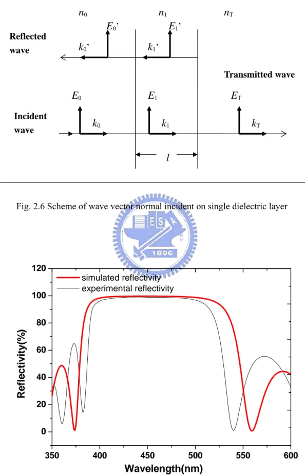
Fig.2.6 Scheme of wave vector normal incident on single dielectric layer…………..14
Fig.2.7 The experimental and simulated reflectivity of 6 pairs TiO2/SiO2 DBRs…....14
Fig.3.1The epitaxial structure of the GaN-based wafer consists of a 30-nm nucleation layer, 4-µm undoped GaN, a multiple quantum-well (MQW) composed of 10 periods of 5-nm GaN barrier and 3-nm In0.1Ga0.9N well, and 280 nm undoped GaN………19
Fig.3.2 The reflectivity of 6 pairs TiO2/SiO2 DBR measured by a n&k analyzer…....19
Fig.3.3 After the residual Ga were removed, the mean surface roughness of the GaN surface measured by atomic force microscopy (AFM) was about 15 nm over a scanned area of 5×5 µm2………..20
Fig.3.4 Scanning electron microscope images of the LLO GaN surface (a) before and (b) after HCl dip……….20
Fig.3.5 The mean surface roughness of the polished GaN surface measured by atomic force microscopy was about 1 nm over a scanned area of 10×10 µm2……..21
Fig.3.6 The reflectivity of the 8 pairs SiO2/Ta2O5 DBR measured by a n&k analyzer………..21
Fig.3.7 (a) The complete structure of the GaN VCSEL with two dielectric DBRs (b) the microscopic top view image of the VCSEL array………22 Fig.3.8 (a) Deposition of 6 pairs TiO2/SiO2 DBR (b) definition of SiO2/TiO2 DBR
mesas by wet etching (c) epoxy bonding process (d) laser lift-off process (e) polishing using diamond slurries (f) deposition of 8 pairs Ta2O5/SiO2
DBR………23 Fig.3.9 (a) The LLO GaN surface after ICP etching without pre-polished by diamond slurries (b) the LLO GaN surface has been lapped by diamond slurries before ICP etching with the same ICP etching recipe. The right part is the region after ICP etching and the left part is the region before ICP etching………..24 Fig.3.10 The equilibrium pressure temperature curve for GaN under N2 ambient,
determined experimentally by Ref [3.4]……….24 Fig.3.11 Pressure-temperature curve for GaN. Shaded region is area where GaN
decomposes at 1250 K.[3.8]……….25 Fig.3.12 The schematic diagram of a laser lift-off process……….……….25 Fig.3.13 The schematic diagram of the setup to measuring the photoluminescence (PL)
spectrum by a He-Cd laser………...26 Fig.3.14 The schematic diagram of the setup for optical pimping by a Nd:
Yttrium-Vanadium-Oxide (YVO4) laser at 355 nm, with a repetition rate of 1 kHz and pulse width of 0.5 ns………...26 Fig.4.1 The PL spectra of as-grown GaN wafers. It showed the emission peak
centered at 414nm with FWHM of 18nm,……….33 Fig.4.2 The PL spectra of cavity with only one side high reflectivity DBR, which was
named as structure I, and the inset is the layer structure of structure I……..33 Fig.4.3 The PL spectra of the complete VCSEL structure, which was named as
structure II, and the inset is the layer structure of structure II………34 Fig.4.4 The related PL spectra of structure I……….……...34 Fig.4.5 The related PL spectra of structure I and structure II with a cavity length of
about 1.66μm………35 Fig.4.6 The simulated reflectivity and experimental PL spectrum of a GaN-based
micro-cavity………...………35 Fig.4.7 This diagram showed the complete structure of the GaN-based VCSELs with
two dielectric DBRs and the direction of collected emission light for PL spectra or emission images……….36 Fig.4.8 Laser emission intensity and FWHM of emission wavelength as a function of the pumping energy operated at room temperature. The threshold pumping energy is about 270 nJ………36
Fig.4.9 Emission spectra from the GaN-VCSEL at various pumping energy. The lasing emission wavelength is 414 nm with a linewidth of 0.25 nm……….37 Fig.4.10 Emission images of cracks on low quality GaN-based LED without DBR
structure (a)below and (b)above the lasing threshold………37 Fig.4.11 The PL spectra of cracks on low quality GaN-based LED without DBR
structure below the lasing threshold and above the lasing threshold……….38 Fig.4.12 Near field emission images of a single GaN-based VCSEL at various
pumping energy of 0.2Eth, 0.9Eth, 1.2 Eth, and 1.3 Eth for Fig. 4.12(a),
4.12(b), 4.12(c), and 4.12(d), respectively. The light emission from the circular disk area depict the laser emission pattern………..38 Fig.4.13 Laser emission patterns from a single GaN-based VCSEL at pumping energy of 1.3 Eth. (a) 2-D emission intensity profiles with a near-Gaussian
distribution. (b) 3-D distribution emission distribution of laser emission….39 Fig.4.14 Transmitted output power of VCSEL versus Polarizer rotation angle. Imax is
maximum transmitted output power and Imin is minimum transmitted output
power………39 Fig.4.15 The variation of the lasing threshold as a function of temperatures is plotted
and the solid line represents the best fit of the experimental data…………40 Fig.4.16 Input-output characteristic on logarithmic scales. Dash line are the
Chapter 1 Introduction
The group III-nitride wide band gap semiconductors have recently attracted considerable interest due to their potential applications in optoelectronics devices, such as laser diodes (LDs) and light emitting diodes (LEDs). Compared to gas or solid-state lasers such as the He-Cd and Nd:YAG laser, the semiconductor laser diode offers considerably smaller size, wide tunable range, higher efficiency with lower power requirements, long lifetime, potentially lower cost, and the unique ability to achieve high speed modulation by simply changing the injected current of the device.[1-2]
Although semiconductor lasers have invented since 1962 and used in so many fields, before 1999, the wavelengths of available commercialized semiconductor lasers lack blue light. The first diode laser at short visible wavelength (in the blue-green, 480-520nm) was demonstrated actually in ZnSe and related II-VI alloys a decade ago, but these have not met the crucial yardstick demanded of a technologically viable device: long component lifetime.[3] Therefore, the attention was paid on the other material-GaN , a class of so-called wide bandgap semiconductors with highly chemical stability and long life time. The related materials, AlGaN and InGaN, are also compositionally adjustable over the near-ultraviolet and visible ranges. The first nitride diode laser, operating at about 420 nm, was demonstrated in 1995 by Nakamura and coworkers at Nichia Chemical Industries in Japan. Nichia has subsequently commercialized the GaN based edge emitting laser and made it available since 1999. [4-5]
Recently, the realization of GaN-based blue/violet vertical cavity surface emitting lasers have attracted much attention because VCSELs have many advantageous properties over the edge emitting laser and applications as follow:[6]
Advantages of VCSELs:
(1) Two-dimensional array configuration. (2) Low threshold currents.
(3) Circular and low divergence output beams (4) High fiber-coupling efficiency.
(6) Lower temperature-sensitivity compared to edge-emitting laser diodes. (7) High transmission speed with low power consumption
Applications:
(1) High density optical storage (2) Optical fiber communication
(3) High-resolution laser printing and so on.
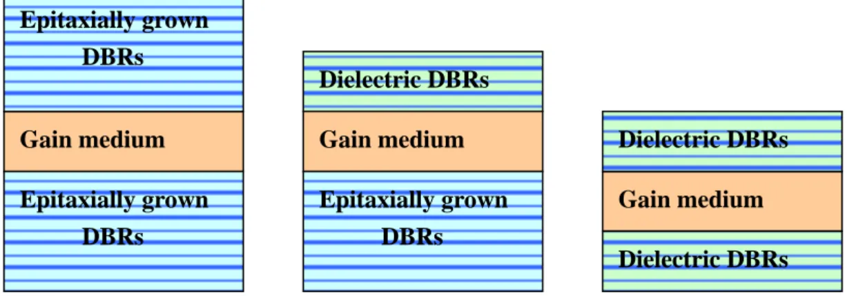
For a GaN-based VCSEL, there are three different approaches to form distributed Bragg reflector (DBR) structures. First is the epitaxially grown GaN/AlGaN DBRs, second is the combination of an epitaxially grown DBRs and a dielectric DBRs, and third is the two dielectric DBRs, as shown in Fig. 1.1. The second approach has been reported recently by T. Someya et al. [7]. The third approach was reported by Y.K. Song et al. [8] using two dielectric SiO2/HfO2 DBRs,
and T. Tawara et al. [9] using two wafer fused dielectric DBRs consisting of SiO2/ZrO2 stacks.
The first and second approaches are relatively difficult to fabricate a cavity structure with high Q factor and low loss due to the bottom epitaxially grown GaN/AlGaN DBRs. The important problems are resulted from that a large number of pairs are required to form high reflectivity DBRs (above 99%) for reducing the lasing threshold because of the small difference of refractive index between the AlGaN and GaN. Then, the roughness and cracks are generated by increasing thickness in these Al-containing DBRs due to the increase of strain. Besides, the crystalline quality of the QWs grown on such DBRs deteriorates.
Therefore, VCSELs were fabricated using the third method in our experiments. This method has many advantages and the main advantage is that we can easily get high quality dielectric DBRs with high reflectivity and without any cracks using evaporation or sputter.
However, a laser lift-off technique and a wafer bonding technique are demanded to transfer a GaN-based film from sapphire substrates to second substrates before deposition of second DBRs for the third approach. Besides, a polish process should be developed to smooth the laser lift-off GaN surface for optical flatness.
In this research, the fabrication and analysis of GaN-based VCSELs were investigated. In the chapter 2, the related theory of DBR and resonant cavity including
cavity mode, laser condition, finesse factor, quality factor and characteristic temperature are introduced. In the chapter 3, we introduce the processes of VCSELs including a laser lift-off technique for GaN-based material and the measurement instruments used in our experiments. The chapter 4 is mainly divided into two parts. First, characteristics of micro-cavity including photoluminescence spectra, simulation of reflectivity and simulation of cavity mode positions are described. Second, the lasing action of laser lift-off GaN-based VCSELs with an In0.1Ga0.9N/GaN multiple
quantum wells (MQWs) and two dielectric DBRs under optical pumping at room temperature are analyzed. Finally, our conclusions and future work are mentioned in the chapter 5.
Figures of chapter 1
Dielectric DBRs Gain medium Epitaxially grown DBRs Gain medium Gain medium Epitaxially grown DBRs Epitaxially grown DBRs Dielectric DBRs Dielectric DBRsFig. 1.1 For GaN-based VCSELs, there are three different approaches to form DBR structure. The cavity can be formed by (a)two epitaxially grown GaN/AlGaN DBRs (b) an epitaxially grown distributed Bragg reflectors (DBRs) and a dielectric DBRs (c) two dielectric DBRs
Chapter 2 Related theories of resonant cavities and Bragg
distribution reflectors
2.1 Ingredients of the laser
The word LASER is an acronym for Light Amplification by Stimulated Emitting of Radiation. To form the “laser”, there are three ingredients: [10]
(1) Gain medium: The gain medium consists of materials which normally absorb incident radiation over some wavelength range. But, if it is pumped by inputting either electrical or optical energy, the electrons within the material can be excited to the higher, nonequilibrium energy level, so that the incident radiation can be amplified rather than absorbed by stimulating the de-excitation of these electrons along with the generation of additional radiation. If the resulting gain is sufficient to overcome the losses of some resonant optical mode of the cavity, this mode is said to have reached threshold, and relatively coherent light will be emitted.
(2) Pumping source: Pumping source provides the energy that can excite the electrons within gain medium at lower energy level to higher energy level. It could be either optical or electrical energy.
(3) Resonant cavity: The resonant cavity provides the necessary positive feedback for the radiation being amplified, so that a lasing oscillation can be established and sustained above threshold pumping level.
In our experiment, the resonant cavity is a key point. Therefore the following sections mainly describe the optical characteristics of resonant cavities and some basic concepts of the Bragg distribution reflectors which are usually used to form cavities.
2.2 Resonant cavity
In order to produce a large amplification, the light has to pass a long length of the gain medium in the laser. Obviously, the most practical way to get light to pass through a long length of the laser medium is by putting mirrors on both sides of the laser medium. These two mirrors form an optically resonant cavity.
The amplitude distribution of an optical wave along the axis of the cavity is illustrated schematically in Fig 2.1.
Constructive interference of the waves within the cavity is required for laser action. The result is the condition of resonance: light waves are amplified strongly if, and only if, they satisfy the equation (2.1),
2nL=Nλ, (2.1) where L is the cavity length, n is the refractive index of the laser medium, nL is the so-called optical path, N is an integer and λ denotes the wavelength.
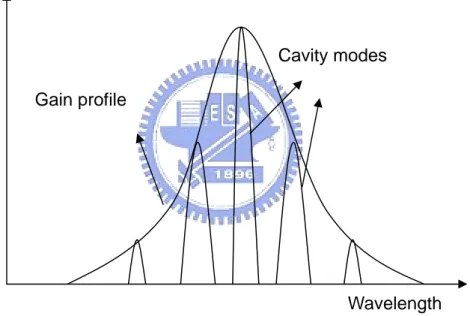
The integer N cannot be an arbitrary number. The gain of laser of the laser medium is also a function of the wavelength, G(l). Laser oscillation can only take place when the gain is large enough to maintain the resonance. Consequently, as shown in Fig. 2.2, the actual profile of wavelength emitted by a laser is the product of the envelope of longitudinal oscillation modes and the gain profile.
The distance between the modes can be obtained from equation (2.2).[11]
nL 2 2 Mode λ λ = ∆ (2.2) Considering dispersion effect, the equation is transformed into
L ne Mode 2 2 λ λ = ∆ (2.3) where (1 ) λ λ d dn n n
ne = − is effective index of refraction including dispersion. And the frequency difference between each longitudinal mode is
L n c or nL c e 2 2 = ∆ν (2.4) c is the light speed. From mode spacing we can calculate the cavity length of laser diode.
2.2.2 Laser conditions
An optical cavity is required to achieve laser action. The cavity causes the amplification of the stimulated emission process in the active medium. The degree of amplification is measured as gain and is expressed as
x I I G d d 1 = . (2.5)
where I is the light intensity and x is the distance of light travel.
The intensity after the light beam travels the distance x can be written as Gx
e I x
I( )= 0 (2.6)
where I0 is the initial light beam at x=0. The intensity increases exponentially as the
light beam propagates through the amplification medium.
Assume that the length of the laser medium within an optical cavity is La; the
cavity length is Lc; absorption of material inside the cavity is α; the reflectances of
the two mirrors are R1 and R2, as shown in Fig 2.3. Then, the intensity of the light after
a round trip in the cavity is given by
) ( 2 0 2 1 a c L GL e I R R I = +α (2.7) To maintain the amplification of the stimulated emission, it is required that
0
I
I ≥ . (2.8) This leads to the condition for lasing
) 1 ln( 2 1 2 1R R L L L G a a c th ≥α +
(2.9)
2.2.3 Finesse factor and quality factor
The Q factor or quality factor is a measure of the "quality" of a resonant system. Quality factor is defined as
cycle per loss energy cavity the in energy stored Q= 2π( ) (2.10) High quality factor indicates high ratio of energy stored to energy dissipated in the cavity and the low lasing threshold.
Assume that the average time of photo in cavity (photo lifetime) is tc and stored
energy in cavity is ε. Then, energy loss per time is expressed as
c t dt dε ε − = (2.11) Using this definition of quality factor and equation (2.10), quality factor can be given by c c t wt d w Q=− εε = =2πν (2.12)
where ν is resonant frequency and ω is angular frequency.
Assume that Δν1/2 is transmittance full-width at half-maximum in units of frequency. The relation betweenΔν1/2 and tc given by
c t π ν 2 1 2 / 1 = ∆ (2.13) Then, we rewrite equation (2.12) by using equation (2.13) as
2 / 1 ν ν ∆ = Q (2.14) The cavity finesse is defined as the ratio of the transmittance peak separation to the transmittance full-width at half-maximum.
2 / 1 mod ν ∆ = = total l c linewidth spacing e F (2.15) where ltotal is distance of one round trip in cavity. Inspection of equation (2.14) and
equation (2.15), Q factor is related to finesse of the cavity by F l F c l Q total total λ ν = = (2.16) where λ is the wavelength of light.[12]
2.2.4 Characteristic temperature
The threshold pumping power of lasers is a function of the operating temperature. The threshold pumping power changes with the temperature, a semi-empirical relation between them, can be expressed as:
0 )
( TT
th T P e
P = × (2.17)
where P is a constant, Pth(T) is the threshold optical pumping power, T is the operating
temperature and T0 is characteristic temperature. So we can get
1 0 [ln( )] − = P P T T th (2.18) According to equation (2.17), the high characteristic temperature indicates the variation of threshold condition is insensitive to the variation of ambient temperature.
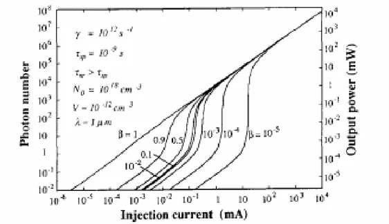
2.2.5 The spontaneous emission factor (β)
∑
= i i A A0 β (2.19)where Ai is the spontaneous emission rate of the active material into mode i and index
0 indicates the optical mode which will eventually lase.
The pump current as a function of the photon number can be expressed as ] ) 1 )( 1 ( 1 [ p p p p q I nr sp ξβ τ τ β ξ β γ − + + + + = (2.20) where I is the injection current, p is the photo number, q is the electron charge, τsp is
the spontaneous emission lifetime, τnr is the nonradiative recombination lifetime, γ is
the cavity decay rate and ξ is a dimensionless parameter defined by
sp V N γτ β ξ = 0 (2.21)
N0 is the transparency carrier concentration of gain material and V is the volume of
the active material.
The injection current versus output power curves were drawn, as shown in Fig. 2.4. The parameters of γ, τsp, N0, V and λ are 1012s-1, 10-9s, 1018 cm-3, 10-12 cm-3
and 1000nm, respectively.[13]
If the micro-cavity laser supports only one mode within the its gain bandwidth, and if non-radiative recombination is negligible, then photon emission is the only means of power dissipation and the quantum efficiency of the device must be unity both below and above threshold. In other words, the spontaneous emission factor is unity.
Inspection of Fig. 2.4, the factor could be generally obtained from the difference between the heights of the emission intensities on a logarithmic scale before and after lasing.
2.3 Theory of Bragg distribution reflectors (DBR)
Low threshold gain indicates that lasers can easily achieve the condition of lasing at low threshold pumping power. Inspection of equation (2.9), the threshold gain of laser is able to be reduced by increasing the reflectivity of reflectors.
n0 1 + -n0 1 r = M1M2M3....MN nT 1 (2.26) nT 1 t = M t 1 n0 + -n0 1 r = M nT 1 t -i n1sin kl n0 1 + -n0 1 (E0’ / E0 ) =
cos kl (-i/ n1)sin kl cos kl nT
1
(ET / E0 )
low refractive indices (Fig. 2.5). The reflected waves from each interface will be in phase at the first incident surface and the amplitude of all reflected waves will be added to get high reflectance.[14]
The principle of DBR can be explained with transfer matrix method (TMM). Consider the boundary conditions of normal incidence of a light wave on a single dielectric layer as in Fig.2.6
In Fig. 2.6, the amplitude of the electric vectors of the incident beam, the reflected beam, and the transmitted beam are E0, E0’ and ET respectively. The electric
field amplitudes in the film are E1 and E1’ for the forward and backward traveling
waves, respectively.
The boundary conditions require that the electric and magnetic fields be continuous at each interface. These conditions are expressed as follows,
Above equations can be simplified as:
1 +( E0’ / E0 ) = [cos kl – i(nT / nT)sin kl]ET /E0 (2.22)
n0 - n0 (E0’ / E0 ) = [-in1sin kl + nT cos kl]ET /E0 (2.23)
Rewrite equations (2.22) and (2.23) in matrix form:
(2.24) Simplify equation (2.24) as:
(2.25) In multi-layers situation, we can extend equation (2.25) to N layers :
First Interface Second Interface
Electric field E0 + E0’ = E1 + E1’ E1eikl + E1’e-ikl = ET
Magnetic field H0 – H0’ = H1 – H1’ or n0E0 - n0 E0’ = n1E1 - n1 E1’
H1eikl + H1’e-ikl = HT or
T Tn C Dn Bn An n t + + + = 0 0 0 2 (2.29) T T T T Dn C n Bn An Dn C n Bn An r + + + − − + = 0 0 0 0 (2.28) M1M2M3....MN = M = A B C D
Where M1, M2, M3,……MN, are the transfer matrix of each corresponding film.
(2.27) Thus, the reflectance and transmittance of the N layer films are:
2.3.2 Comparison of simulated and experimental reflectivity of DBRs
In this section, the experimental reflectivity and simulated reflectivity of DBRs were compared.
The 6 pairs TiO2/SiO2 DBRs were deposited on a GaN layer. The thickness of
TiO2 and SiO2 layers were about 45nm and 75nm, respectively. Fig 2.7 shows the
experimental and simulated reflectivity of 6 pairs TiO2/SiO2 DBRs. The experimental
reflectivity and stop band were smaller than simulated reflectivity and stop band due to thickness fluctuation of DBRs and scattering at surface.
Figures of chapter 2
Figure 2.1: Light wave resonance in a cavity.
Mirror 1 Mirror 2
L
Figure 2.2: Several resonant modes can fit within the gain profile. Gain profile
Cavity modes
Wavelength
Figure 2.3 Structure of resonant cavity.
Mirror 2 La Lc Gain medium Mirror 1 R1 R2
n
Hn
Ld
Hd
LdH=λ/4nH dL=λ/4nL
Fig. 2.5: Schematic of a DBR
Fig. 2.4 The injection current versus output power curves are drawn. The parameters of γ, τsp, N0, V and λ are 1012s-1, 10-9s, 1018 cm-3, 10-12
350 400 450 500 550 600 0 20 40 60 80 100 120 simulated reflectivity experimental reflectivity
Ref
lecti
vi
ty(
%
)
Wavelength(nm)
Fig. 2.7 The experimental and simulated reflectivity of 6 pairs TiO2/SiO2 DBRs.
Fig. 2.6 Scheme of wave vector normal incident on single dielectric layer
n
0n
1n
Tk
TE
Tk
1k
0E
1E
0E
0’E
1’k
1’k
0’l
Reflected wave Incident wave Transmitted waveChapter 3 Experimental processes and measurement instruments
3.1 Experimental processes
3.1.1 Processes of VCSELs
The epitaxial structure of the GaN-based VCSEL was first grown on a (0001)-oriented sapphire substrate by metal organic chemical vapor deposition system. The structure consists of a 30-nm nucleation layer, 4-µm undoped GaN, a multiple quantum-well (MQW) composed of 10 periods of 5-nm GaN barrier and 3-nm In0.1Ga0.9N well, and 280 nm undoped GaN as shown Fig.3.1. The original epitaxial
wafer was cleaved to a size of 1.5×1.5 cm2. The backside of the sapphire substrate was polished using diamond slurries in order to reduce scattering of KrF excimer laser during the laser lift-off process. Then a dielectric DBR consisting of 6 pairs of SiO2/TiO2 was evaporated on the top of the grown structure to form a SiO2/TiO2
DBR/InGaN MQW/GaN/sapphire structure. The structure has a reflectivity of 98.3% at 414 nm measured by a n&k analyzer, as shown in Fig. 3.2. Then, an array of disk-like SiO2/TiO2 DBR mesas with 60 µm in diameter was formed by standard
photolithography process and buffer oxide etcher (BOE). The patterned SiO2/TiO2
DBR/InGaN MQW/GaN/sapphire structure was then mounted onto a host fused silica substrate by epoxy bonding processes. The mounted sample was then subjected to a laser lift-off (LLO) process similar to the process we reported earlier [15-16]. A KrF excimer laser at 248 nm was incident on the sapphire substrate to cause the deposition of GaN into gaseous nitrogen and gallium droplets. The average energy density of KrF excimer laser was approximately 600 mJ/cm2. Then, the sapphire was separated from the epitaxilly grown structure to form a GaN/InGaN MQW/SiO2/TiO2
DBR/silica substrate configuration. The transferred sample was dipped into HCl solution to remove the residual Ga on the n-GaN. After the residual Ga were removed, the mean surface roughness of the GaN surface measured by atomic force microscopy (AFM) was about 15 nm over a scanned area of 5×5 µm2, as shown in Fig. 3.3.
Scanning electron microscope images of the GaN surface before and after HCl dip were shown in Fig. 3.4(a) (b). The GaN surface of the lifted-off structure was then lapped and polished by diamond slurries to assure smooth surface for deposition of the second dielectric DBR. After the polish process, a smoother GaN surface with a mean surface roughness about 1nm over a scanned area of 10×10 µm2 was obtained,
than 3nm.
Finally, the second DBR consisting of 8 pairs of SiO2/Ta2O5 was deposited on
the top of the polished GaN surface. The reflectivity of the SiO2/Ta2O5 DBR at 414
nm is 97.2% measured by a n&k analyzer, as shown in Fig. 3.6. The complete structure of the GaN VCSEL with two dielectric DBRs is shown in Fig. 3.7(a). Fig. 3.7(b) shows the microscopic top view image of the VCSEL array, the circular disk areas are the location of VCSELs with DBR cavity. Fig. 3.8(a)-(f) show the fabrication steps of the optically pumped GaN- based blue-violet vertical cavity surface emitting laser using wafer bonding and LLO techniques.
3.1.2 Issues of processes for reduction of cavity lengths
The numbers of cavity mode and threshold gain are related to cavity length. Therefore, the cavity length is demanded to be controlled. ICP etching is a good method to control cavity lengths more exactly than lapping with diamond slurries. The interface between the GaN layer and sapphire substrate is named as LLO surface when the sapphire is removed from bulk GaN layer by a laser lift-off technique. Fig. 3.9(a) shows the LLO GaN surface after ICP etching without pre-polished by diamond slurries and the etching was conducted under a gas mixture condition of Cl2/Ar = 50/30 standard cubic centimeter min (sccm), the 400W of ICP
source power, 40W of bias power and 0.66Pa of chamber pressure for a 1 min etching time. In Fig. 3.9(b), the LLO GaN surface has been lapped by diamond slurries before ICP etching with the same ICP etching recipe. The right part of Fig. 3.9(b) is the region after ICP etching and the left part is the region before ICP etching.
Inspection of Fig. 3.9, the smoother surface (RMS~1nm) of LLO GaN surface with pre-polished was obtained after ICP etching. This is partly because the mean surface roughness (RMS~15nm) of a LLO GaN surface after wet etching is rougher than that (RMS<1nm) of an epitaxial GaN surface. In addition, the LLO GaN surface is a highly defective region due to a GaN buffer layer grown on a sapphire substrate at the low temperature.[17] The existence of defect would cause the higher etching rate of the region near defects and result a rough GaN surface after ICP etching.[18] In order to obtain a smooth GaN surface, it is necessary to remove the GaN buffer layer and to smooth the LLO GaN surface by pre-polished before ICP etching.
pre-polished is better than that of the sample without pre-polished.
3.2 Laser lift-off technique
3.2.1 GaN Decomposition
In a report by Sun et al. [19] the thermal decomposition of MOCVD grown GaN on r-plane sapphire was found to occur at a temperature of 1000°C in a hydrogen ambient. They reported that the surface of the GaN thin film was totally decomposed leaving only a residual Ga droplet surface, following the equation:
) ( 2
2
1
gN
Ga
GaN
⇔
+
.Fig. 3.10 shows the equilibrium pressure temperature (P-T) curve for GaN under N2 ambient, determined experimentally by Karpinski et. al.[20] In the recent
report [21-23], the critical temperature of GaN decomposition was estimated to be about 1000℃. The recently report [24-25] also shows the calculated P-T curve for GaN as show in Fig. 3.11. The decomposition of GaN→Ga(l)+N2(g) was occurred at
a critical temperature of ~1000℃ at 1 atm. The GaN sample after laser irradiation tends to show some material residues such as Ga, and Ga oxide. These residues were then clean up by dilute acid solution such as HCl or H2SO4/H2O2. Besides, structural
damage and chemical intermixing resulting from laser processing was minimal and that was confined to approximately the first ≅ 50nm of the resulting material.[26]
3.2.2 KrF excimer laser setup
Fig. 3.12 shows the schematic diagram of the setup for conducting the LLO experiment. A KrF excimer laser (Lambda Physick LPX210) at wavelength of λ=248 nm with pulse width of 25 ns was used for LLO technique. The maximum laser output energy was about 700 mJ. The frequency of laser can be varied from 1 Hz to 100Hz. The LLO processing beam passed through a optical projection system, and then focuses onto the sample with a square spot size of 1.2×1.2 mm2. The samples were placed on the top of working station which can be moved by hand. The decomposition of GaN→Ga(l)+N (g) was occurred at the interface between a GaN layer and a
substrate was easily remove from the LEDs structure by heating the irradiated sample at a Ga melting point of about 30℃.
3.3 Optical measurement instruments
3.3.1 μ-PL systems
Fig. 3.13 shows the schematic diagram of the setup for measuring the photoluminescence (PL) spectrum of samples using a He-Cd laser. The He-Cd laser output power at wavelength of λ=325 nm was about 24mW under continuous wave operation. The laser beam passed through some optical lenses and mirrors, and then was normally incident onto the sample surface with a focused spot size of about 2 µm in diameter. The light emission was collected into a spectrometer (Jobin-Yvon Triax 320) with a resolution of 0.1 nm. Besides, the emission images of samples and the position where the laser beam located on samples could be measured using a charge couple device (CCD).
3.3.2 Optical pumping systems
Fig. 3.14 shows the schematic diagram of the setup for optical pimping by a Nd: Yttrium-Vanadium-Oxide (YVO4) laser at 355 nm, with a repetition rate of 1 kHz and pulse width of 0.5 ns. The maximum of average laser output power was about 17mW. The laser beam with a focused spot size of about 40 µm in diameter was normally incident on the sample surface and the light emission from the sample was collected using an imaging optic into a spectrometer (Jobin-Yvon Triax 320) with a resolution of 0.1 nm, and measurement by a charge couple device (CCD). The setup of optical pumping system is similar to the setup of a µ-PL system.
Figures of chapter 3
4um n-GaN
Sapphire 280nm GaN cap layer
InGaN/GaN MQW 10pairs
Fig.3.1. The epitaxial structure of the GaN-based wafer consists of a 30-nm nucleation layer, 4-µm undoped GaN, a multiple quantum-well (MQW) composed of 10 periods of 5-nm GaN barrier and 3-nm In0.1Ga0.9N well, and
280 nm undoped GaN
Fig.3.2. The reflectivity of 6 pairs TiO2/SiO2 DBR measured by a n&k analyzer.
350 400 450 500 550 600 0 20 40 60 80 100 120
6 pairs TiO2/SiO2 DBRs
Re fl ec tance(% ) Wavelength(nm)
Ga
(a) (b)
Fig.3.4. Scanning electron microscope images of the LLO GaN surface (a) before and (b) after HCl dip
RMS : 15~20 nm
Fig.3.3. After the residual Ga were removed, the mean surface roughness of the GaN surface measured by atomic force microscopy (AFM) was about 15 nm over a scanned area of 5×5 µm2
Fig.3.5. The mean surface roughness of the polished GaN surface measured by atomic force microscopy was about 1 nm over a scanned area of 10×10 µm2
Fig.3.6. The reflectivity of the 8 pairs SiO2/Ta2O5 DBR measured by a n&k
350 400 450 500 550 600 0 20 40 60 80 100 120 8 pairs Ta2O5/SiO2 DBRs Re fl e c tance(% ) Wavelength(nm)
GaN film
Glass substrate DBR
Epoxy
(a) (b)
Fig.3.7. (a) The complete structure of the GaN VCSEL with two dielectric DBRs (b)the microscopic top view image of the VCSEL array
GaN film Sapphire DBR (a) GaN film DBR Glass substrate Epoxy (f) DBR DBR (b) GaN film Sapphire DBR 60μm DBR GaN film Sapphire DBR Glass substrate (c) DBR (d) Sapphire GaN film DBR Glass substrate Epoxy KrF excimer laser DBR GaN film DBR Glass substrate Epoxy (e) DBR Diamond slurry
Fig.3.8. (a) Deposition of 6 pairs TiO2/SiO2 DBR (b) definition of SiO2/TiO2
DBR mesas by wet etching (c) epoxy bonding process (d) laser lift-off process (e) polishing using diamond slurries (f) deposition of 8 pairs Ta2O5/SiO2 DBR
Figure. 3.10: The equilibrium pressure temperature curve for GaN under N2 ambient, determined experimentally by Ref [3.4].
(a) (b)
Non-etched
etched
Figure. 3.9: (a)A SEM image of GaN surface after ICP etching without pre-polish (b) a SEM image of GaN surface with pre-polish. The right part is the region after ICP etching and the left part is the region before ICP etching.
Figure 3.11: Pressure-temperature curve for GaN. Shaded region is area where GaN decomposes at 1250 K.[3.8]
Mirror
Lens
Work station
KrF excimer laser
He-Cd laser(325nm)
sample dichroic mirror Objective 15X x-y PZT scan stage flip mirror CCD tube lens Spectrograph CCD fiberSNOM
SNOM
PMTHe-Cd laser(325nm)
sample dichroic mirror Objective 15X x-y PZT scan stage flip mirror CCD tube lens Spectrograph CCD Spectrograph CCD fiberSNOM
SNOM
PMT PMTFig.3.13. The schematic diagram of the setup to measuring the photoluminescence (PL) spectrum by a He-Cd laser.
Fiber Spectrometer (resolution=1Å) Dichroic mirror Objective (40X) CCD detector Sample Computer Nd:YVO4 355nm pulse laser Objective (15X) Mirror 410 412 414 416 418 420 0 200 400 600 800 1000 P=1.07Pth E m is s ion I n te ns it y (a .u.) Wavelength(nm) Emission spectra Ta2O5/SiO2DBR TiO2/SiO2 DBR MQW Emission images
Fig.3.14. The schematic diagram of the setup for optical pimping by a Nd: Yttrium-Vanadium-Oxide (YVO4) laser at 355 nm, with a repetition rate of 1 kHz and pulse width of 0.5 ns.
Chapter 4 Results and discussions
4.1 Characteristics of a GaN-based microcavity
4.1.1 Photoluminescence spectra
The photoluminescence (PL) spectra of the VCSELs were measured using a µ-PL system. The pumping source was a He-Cd laser with the wavelength of 325nm. Prior to the fabrication of GaN-based microcavity, we measured the PL spectra of as-grown GaN-based wafers and it showed the emission peak centered at 414nm with FWHM of 18nm, as shown in Fig. 4.1. The inset in Fig 4.1 is the structure of measured wafers.
Fig. 4.2 shows the PL spectra of cavity with only one side high reflectivity DBR, which was named as structure I, and the inset is the layer structure of structure I. A clearly modification of the emission peak caused by cavity effect was observed. It shows that the DBR would not be degraded in bonding and laser lift-off processes. The PL intensity (between 410-420nm) of a multiple quantum-well (MQW) layer was smaller than that (at 365nm) of a GaN layer due to scattering and absorption of the pumping source (a He-Cd laser) by the GaN layer.
Estimated effective refractive index (n-dn/dλ) of about 3.4 was obtained by substituting known experimental data (cavity length=4μm; peak wavelength=410nm; free spectral range=6.5nm) shown in Fig 4.2 into equation (4.1), where L is cavity length, λ is peak wavelength, λFSR is free spectral range (wavelength spacing between
the longitudinal cavity modes) and n is refractive index. The value of 3.4 generally consists with the value used in previous reports. [27]
L d dn n FSR ) ( 2 2 λ λ λ − = (4.1) The Fig. 4.3 shows the PL spectra of the complete VCSEL structure, which was named as structure II, and the inset is the layer structure of structure II. The FWHM of cavity modes around 450nm was about 1nm and the value of quality factor (Q factor) was about 450 calculated by equation 4.2, where λ is peak wavelength and Δλ is FWHM of the peak wavelength. Although the cavity modes can be clearly seen in the figure, the PL intensity of a multiple quantum-well (MQW) layer was very weak.
λ
=
In order to enhance the PL intensity of MQW layer, it is inevitable to reduce the thickness of the GaN layer to eliminate absorption for the pumping power of a He-Cd laser. Therefore, we reduced thickness of the GaN layer and investigated the PL intensity ratio of MQW layer and GaN layer. In this experiment, the samples with four different thicknesses of GaN layers were fabricated by a lapping process. The related PL spectra of structure I were measured, as shown in Fig 4.4. The thicknesses of GaN films were estimated using equation (4.1) and the effective index. We observed the PL relatively intensity of the MQW layer enhanced compared to that of the GaN layer and mode spacing increased as we reduced the cavity length. When the cavity length was reduced to 1.66um, the PL intensity of the MQW layer was stronger than that of the GaN layer. The related PL spectra of structure I and structure II with a cavity length of about 1.66μm were shown in Fig. 4.5. The FWHM of the cavity mode around 430nm reduced from 7nm to 1.2nm and Q factor was improved from 60 to 360 due to the high reflectivity of reflectors. The high value 360 of Q factor indicated a high quality resonant cavity was fabricated.
4.1.2 Simulation of reflectivity for GaN-based microcavity
The reflectivity of GaN-based VCSELs were simulated using TF Calc thin film design software in order to compare with our experiments.[28]
Figure 4.3 shows the simulated reflectivity of structure II with a resonant cavity length of 1.63um and experimental PL spectrum of structure II with an estimated cavity length of 1.66um. In the Fig. 4.6, the dip positions of simulated reflectivity matched the emission peak positions and the estimated cavity length almost consisted with the simulated cavity length. It is an evidence that the modification of PL spectra were resulted from the cavity effect and makes sure the correctness of estimated cavity length.
The dips of simulated reflectivity did not have the same depth in Fig. 4.6 because the numbers of data points were not enough to describe dips clearly. The spacing between simulated points of reflectivity was 0.1nm.
4.1.3 Correctness of effective refractive index
In this section, the more powerful evidences, SEM images, than simulation were presented to make sure the correctness of estimated cavity length.
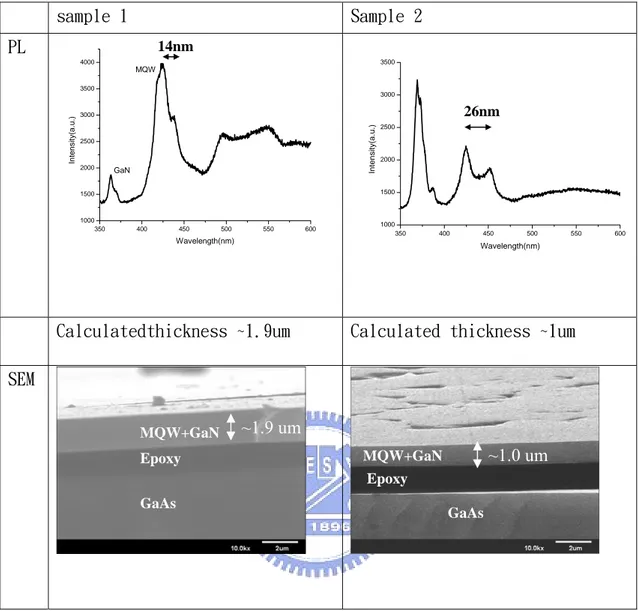
In this experiment, the samples with two different thicknesses were fabricated by a lapping process. The structure of samples consisted of a GaN layer with varied thickness, a multiple quantum-well (MQW) composed of 10 periods of 5-nm GaN barrier and 3-nm In0.1Ga0.9N well, and 280nm GaN layer fabricated on a GaAs
substrate. The related SEM images, PL spectra and estimated thickness of GaN films were measured and arranged, as shown in table 4.1. The consistency between the calculated thickness and the actual thickness supports the correctness of our estimated effective refractive index (about 3.4).
4.2 Optical pumping of VCSELs
4.2.1 Emission spectra
The fabricated GaN-based VCSELs were optically pumped with a Nd: Yttrium-Vanadium-Oxide (YVO4) laser at 355 nm, with a repetition rate of 1 kHz and
pulse width of 0.5 ns. The pumping laser beam with a focused spot size of about 40µm in diameter is vertically incident on the VCSEL sample from the SiO2/ Ta2O5
DBR side and the light emission from the VCSEL sample was collected using an imaging optic into a spectrometer (Jobin-Yvon Triax 320) with a resolution of 0.1 nm, and measurement by a charge couple device (CCD) as depicted in Fig.4.7.
Fig. 4.8 shows the laser emission intensity and FWHM of the emission spectrum as a function of pumping energy at room temperature conditions. A clear evidence of threshold condition occurs at pumping energy of 270 nJ corresponding to an energy density of 21.5 mJ/cm2. The laser intensity increases linearly with the pumping energy level beyond the threshold energy. The estimated carrier density at threshold is in the order of 1020 cm-3 assuming a reflectivity of 35% for the SiO2/Ta2O5 DBR at the pumping wavelength of 355 nm and absorption in 4-µm GaN
layer of 97 %. According to the report by Park [29], the gain coefficient of InGaN at this carrier density level is about 104 cm-1. We estimated the threshold gain (gth) value
of our VCSEL using equation (4.3) where L is the total thickness of the wells in InGaN MQWs and R1 and R2 are the reflectivity of the DBRs. We obtained an
estimated gain coefficient of about 104 cm-1 which is consistent with the above g th
value estimated from the carrier density.
) 1 ln( 1
Fig. 4.9 shows the evolution of the VCSEL emission spectrum with the pumping energy at room temperature. At below threshold pumping energy, the spontaneous emission spectrum shows a multiple cavity modes with a mode spacing of about 7 nm and a linewidth of about 0.8 nm. This mode spacing corresponds to a cavity length of 3.5 µm. The cavity Q factor estimated from the linewidth is about 518. An estimated effective cavity reflectivity based on this Q factor is about 97% which is close to the cavity reflectivity formed by the two dielectric DBRs. This result indicates the laser cavity structure was nearly intact after the laser lift-off process. As the pumping energy increases above the threshold, a dominant laser emission line appears at 414 nm with a narrow linewidth of about 0.25 nm.
4.2.2 The near –field patterns and far-field patterns
In the optical pumping experiment, we found that the stimulated emission can be easily observed from the cracks or defects on samples due to light resonating in unintentionally cavity formed between cracks or defects and scattered out in the vertical direction. Fig. 4.10(a) and 4.10(b) show emission images of cracks on low quality GaN-based LEDs without DBR structure below and above the lasing threshold, respectively. In the Fig. 4.10(b), intense light which originates above the lasing threshold is clearly seen from creaks. Fig. 4.11 shows the emission spectra of cracks on low quality GaN-based LEDs without DBR structure below and above the lasing threshold.[30] Inspection of Fig. 4.11, the cavity modes resulted from cracks were random and unpredicted.
Therefore, our laser action of a GaN based VCSEL caused by a vertical resonant cavity should be clarified. In this section we studied the near field patterns and far field patterns of the laser emission. The near field patterns of laser emission were measured from the pattern DBR side by using microscope with a color CCD under different pumping energy conditions, as shown in Fig. 4.7. Fig. 4.12(a), 4.12(b), 4.12(c), and 4.12(d) show the images at pumping energy of 0.2Eth, 0.9Eth, 1.2 Eth, and
1.3 Eth, respectively. Fig. 4.12(a) and 4.12(b) show the spontaneous emission images
of the VCSEL. The brighter ring in these images were caused by the scattering light from the side wall of the patterned DBRs and the burred emission outside the patterned area could be the fluorescence of the sample. With the pumping energy increased above the threshold energy, a bright emission appears inside the circular
disk area of the VCSEL structure. However, no similar bright emission was observed outside the circular area. This result clearly indicated the onset of the vertical laser emission from the VCSEL cavity.
Fig. 4.13(a) shows the 2-D contour plot of the spatial intensity distribution of the laser beam. The cross section profiles (white curves) show a near-Gaussian intensity distribution in both axes. Fig. 4.13(b) shows the 3-D isometric plot of the spatial intensity distribution of the laser beam. If the laser beam originated from a horizontal resonant cavity and was scattered in the vertical direction of devices, the beam shape in far-field emission images would be irregular. Therefore, the circular beam shape in the far field image is an evidence to prove that the laser is emitted from the vertical resonant cavity.
Besides, the divergence angle was estimated to be about 10 ゚ using the beam size in far-field emission images and focus distance of the objective. This divergence angle ~10 ゚ generally consisted with that reported by Y. K. Song et al.[31]
4.2.3 Polarization
A polarizer was placed in front of the spectrometer in the optical pumping system and the emission spectra of VCSELs were measured at variable angle of the polarizer.
The laser emission intensity as a function of the angle of the polarizer was described as shown in Fig 4.14. The solid line in the figure is the fitting curve which follows the function of cos2θ, where θ is the polarizer rotation angle. The intensity of ideal linear polarized light transmitted through a polarizer is the function of cos2θ. In Fig 4.14, it can be seen the experimental data partially matched the fitting curve. Besides, the results showed a degree of polarization of about 70% estimated using equation (4.4), where Imax is maximum transmitted output power and Imin is minimum
transmitted output power. The value of about 70% and partial a cosine square variation suggest a strong linear polarization property of VCSELs.
min max min max deg I I I I ion polaerizat of ree + − = (4.4)
4.2.4 Characteristic temperature
less sensitive to change in temperature. It is well known that high-temperature sensitivity of the lasing threshold usually limits the performance of a laser under high-temperature operation. On the other hand, weak temperature dependence for the lasing threshold implies that the high-temperature performance limit for laser operation can be significantly expanded.[32]
The variation of the lasing threshold as a function of temperature is plotted in Fig. 4.15. The solid line in Fig. 4.15 represents the best fit of the experimental data to the empirical form (4.5) for the temperature dependence of the lasing threshold.
0 0 ~ ) ln( T T I Ith (4.5)
where I0 is a constant, Ith is the threshold optical pumping power, T is the operating
temperature and T0 is characteristic temperature.
The characteristic temperature T0 was estimated to be 278 K over the
temperature range from 80 to 300 K for our VCSELs. This value of T0 for GaN based
VCSELs is slightly lower than the estimated value of ~300K reported by Iga et al.[33] This is probably because the experimental T0 might be suppressed by leakage currents
and non-radial recombination which was not considered in the modal theory occurred in the active layer.
4.2.5 The spontaneous emission factor (β)
The spontaneous emission factor (β) indicates the coupling efficiency of the spontaneous emission to the lasing mode. This factor could be generally obtained from the difference between the heights of the emission intensities on a logarithmic scale before and after lasing. Therefore, Fig. 4.16 replots the emission intensities shown in Fig. 4.8 on a logarithmic scale and the value of the spontaneous emission factor β is about 10-3. The value of β (~10-3) is smaller than the value of about 10-2
mentioned in others’ papers.[34-35] This is partially because the cavity length of our devices are larger than that of their devices and the spontaneous emission factor (β) decreases with a raise in the cavity mode volume.
Figures of chapter 4
350 400 450 500 0 2000 4000 6000 8000 10000 FWHM=18nm In tensit y (a. u. ) Wavelength(nm)Fig.4.1. The PL spectra of as-grown GaN wafers. It showed the emission peak centered at 414nm with FWHM of 18nm, 350 400 450 500 0 2000 4000 6000 8000 10000 MQW GaN In tensi ty (a.u.) Wavelength(nm)
Fig.4.2. The PL spectra of cavity with only one side high reflectivity DBR, DBR
Epoxy
4µm Glass substrate MQW GaN He-Cd laser Sapphire GaN MQW He-Cd laser Structure I350 375 400 425 450 475 0 500 1000 1500 2000 2500 In te nsity (a.u.) Wavelength(nm)
Fig.4.4. The related PL spectra of structure I
380 400 420 440 460 480 500 0 2 4 6 8 10 1.66um 2.2um 2.8um 4.0um(unpolished) In te n s ity (a .u .) Wavelength(nm)
Fig.4.3. The PL spectra of the complete VCSEL structure, which was named as structure II, and the inset is the layer structure of structure II.
Glass 4µm GaN DBR Epoxy DBR MQW Structure II
350 400 450 500 550 600 0 200 400 600 800 1000
Full cavity structure
In te n s ity (a .u .) Wavelength(nm)
Half cavity structure
FWHM=1.2nm FWHM=7nm
Fig.4.5. The related PL spectra of structure I and structure II with a cavity length of about 1.66μm. 350 400 450 500 550 600 0 20 40 60 80 100 120 Simulated reflectivity(%) Intensit y (a. u.) Re fl e c ti vi ty(% ) Wavelength(nm) 0 200 400 600 800 1000 PL of GaN microcavity
Fig.4.7. This diagram showed the complete structure of the GaN-based VCSELs with two dielectric DBRs and the direction of collected emission light for PL spectra or emission images.
host substrate InGaN patterned SiO2/TiO2 DBR SiO2/Ta2O5 DBR pumping laser VCSEL spectra Emission images 8× 15× 50 100 150 200 250 300 350 0 100 200 300 400 500
laser emission intensity
Emi s si on i nt e nsi ty (a. u. ) Exitation energy(nJ/pulse) 0.0 0.5 1.0 1.5 2.0 2.5 FWHM of emission wavelength FWHN(nm)
Fig.4.8. Laser emission intensity and FWHM of emission wavelength as a function of the pumping energy operated at room temperature. The threshold pumping energy is about 270 nJ.
390 400 410 420 430 440 0 500 1000 1500 2000 2500 3000 3500 4000 0.8nm 0.25nm 0.27Pth Pth Emiss ion Intensity (a .u.) Wavelength(nm) 1.07Pth
Fig.4.9. Emission spectra from the GaN-VCSEL at various pumping energy. The lasing emission wavelength is 414 nm with a linewidth of 0.25 nm.
(a)Below threshold (b)Above threshold
Lasing by cracks
Fig.4.10. Emission images of cracks on low quality GaN-based LED without DBR structure (a)below and (b)above the lasing threshold.
50µm (a) (b) (d) 0.2Eth 0.9Eth 1.3Eth 1.2Eth (c) 360 380 400 420 440 0 1000 2000 3000 4000 5000 6000 7000 Below threshold Above threshold In te n s ity (a .u .) Wavelength(nm)
Fig.4.11. The PL spectra of cracks on low quality GaN-based LED without DBR structure below the lasing threshold and above the lasing threshold
Fig.4.12. Near field emission images of a single GaN-based VCSEL at various pumping energy of 0.2Eth, 0.9Eth, 1.2 Eth, and 1.3 Eth for Fig. 4.12(a),
4.12(b), 4.12(c), and 4.12(d), respectively. The light emission from the circular disk area depict the laser emission pattern.
Fig.4.13. Laser emission patterns from a single GaN-based VCSEL at pumping energy of 1.3 Eth. (a) 2-D emission intensity profiles with a near-Gaussian
distribution. (b) 3-D distribution emission distribution of laser emission.
(a) (b)
Fig.4.14. Transmitted output power of VCSEL versus Polarizer rotation
0 50 100 150 200 250 300 350 20 40 60 80 100 120 140 160 180 200 Experimental data Fitting curve Degree (o) In te n s ity (a.u .)
Fig.4.15 The variation of the lasing threshold as a function of temperatures is plotted and the solid line represents the best fit of the experimental data.
50 100 150 200 250 300 6.0 6.2 6.4 6.6 6.8 7.0 7.2 7.4 Experimental data
Linear fit of experimental data
ln (E th /E 0 )(a.u.) Temperature(K)
Fig.4.16 Input-output characteristic on logarithmic scales. Dash line are the theoretical fitting. 50 100 150 200 250 300 350 1E-4 1E-3 0.01 0.1 1 10 100 Int ens it y (a. u. ) Excitation Energy(nJ/pulse)
sample 1 Sample 2 PL
Calculatedthickness ~1.9um Calculated thickness ~1um SEM
Table 4.1. Structure of samples consist of 4μm GaN layer, a multiple quantum-well (MQW) composed of 10 periods of 5-nm GaN barrier and 3-nm In0.1Ga0.9N well, and
280nm GaN layer fabricated on GaAs substrate by laser lift-off technique and bonding technique. The PL spectra, calculated thickness and SEM pictures of samples were arranged in above table.
350 400 450 500 550 600 1000 1500 2000 2500 3000 3500 Inten s ity (a .u.) Wavelength(nm) 350 400 450 500 550 600 1000 1500 2000 2500 3000 3500 4000 MQW GaN Int ensi ty (a. u. ) Wavelength(nm) 14nm 26nm GaAs Epoxy MQW+GaN ~1.9 um ~1.0 um GaAs Epoxy MQW+GaN
Chapter 5 Conclusions and future work
5.1 Conclusions
We have fabricated an optical pumped GaN-based vertical cavity surface emitting laser which was formed by two dielectric DBRs of SiO2/TiO2 and
SiO2/Ta2O5. In order to fabricate resonant cavity with high Q factor, we also
successfully developed a laser lift-off technique to transfer GaN-based film. Besides, we also optimized the recipe of polish process to get optical flatness for deposition of dielectric DBRs. By utilizing above techniques, we fabricated resonant cavity with high Q factor of 518.
The lasing action was obtained from a GaN-based VCSEL with In0.1Ga0.9N/GaN MQWs and two dielectric DBRs of SiO2/TiO2 and SiO2/Ta2O5
fabricated by a laser lift-off technique. The laser emits blue-violet wavelength at 414 nm under optical pumping at room temperature with threshold energy of 270 nJ. The laser emission has a narrow linewidth of 0.25nm and a degree of polarization of 70%. The characteristic temperature of our GaN-based VCSEL is about 278K. The laser emission images, including near-field patterns and far-field patterns clearly indicate the vertical lasing emission of the VCSEL.
5.2 Future work
The optical characteristics of GaN-based VCSELs will be investigated in detail, such as influence of temperature for wavelength and so on. Besides, electrical pumped GaN-based VCSELs would be fabricated in the future. The electrical pumped devices are more useful than optical pumped devices depending on the viewpoint of application. Therefore, we will try to realize electrical pumped VCSEL by developing some extra techniques such as deposition of metal, dry etching and ion implant. However, some difficulties which are not met in optical pumped devices could be anticipated for electrical pumped devices. For example, leakage current and poor electrical properties of contact may be generated during a bonding process. The devices may be damaged by heat before laser threshold. Therefore, we will develop some important techniques as follow:
(2) Ion-implant technique for current confinement (3) Intra-cavity contacts
(4) Thermal annealing technique for ohmic contact and so on to accomplish electrical pumped GaN-based VCSELs.
Reference
[1]H. Kressel, J. K. Butler,”Semiconductor Lasers and Heterojunction LEDs”, Academic Press (1977)
[2]Hui-Yi Li, “Characteristics Measurement of GaN Blue Laser Diode” Master’s Thesis by National Chiao Tung University(2001).
[3]G. Neumark, R. Park, J. DePuydt, Physics Today, 26(1994) [4]S. Nakamura, G. Fasol, The Blue laser diode, Springer (1997)
[5]N. M. Johnson, A. V. Nurmikko, S. P. DenBaars, Physics Today, 31, (2000) [6]Http://www.us-lasers.com/vcsels.htm
[7]T. Someya, R. Werner, A. Forchel, M. Catalano, R. Cingolani, and Y. Arakawa, Science 285, 1905-1906 (1999).
[8]Y.-K. Song, H. Zhou, M. Diagne, A. V. Nurmikko, R. P. Schneider, Jr., C. P. Cuo, M. R. Krames, R. S. Kern, C. Carter-Coman, and F. A. Kish, Appl. Phys. Lett. 76, 1662-1664 (2000).
[9]T. Tawara, H. Gotoh, T. Akasaka, N. Kobayashi, and T. Saitoh, Appl. Phys. Lett. 83, 830-832 (2003).
[10]J. T. Chu, “Study of Wafer Fusion Technique for Fabrication of Long Wavelength Vertical Cavity Surface Emitting Laser” Master’s Thesis by National Chiao Tung University (2004).
[11]Http://kottan-labs.bgsu.edu/teaching/workshop2001/
[12]Bahaa E. A. Saleh and Malvin Carl teich, “Fundamentals of photonics”, John Wiley and Sons (1991)
[13]G. Bjork and Y. Yamamoto, IEEE J. Quantum Electron, 27, 2386 (1991) [14]L.A. Coldren, S.W. Corzine, “Diode laser and photonic integrated circuits”,
John Wiley and Sons (1995)
[15]C. F. Chu, F. I Lai, J. T. Chu, C. C. Yu, C. F. Lin, H. C. Kuo, and S. C. Wang, J. Appl. Phys. 95, 3916-3922, (2004).
[16]J. T. Chu, H. W. Huang, C. C. Kao, W. D. Liang, F. I Lai, C. F. Chu, H. C. Kuo and S. C. Wang, Jap. J. Appl. Phys., 44, 2509(2005)
[17]H. S. Kim, M. D. Dawson and G. Y Yeom, J. Korean Phys. Society, 40, 567(2002) [18]C. C. Yu, C. F. Chu, J. Y. Tsai, H. W. Huang, T. H. Hsueh, C. F. Lin and S. C.
Wang. Jpn. J. Appl. Phys., 41, L 910(2002)
![Figure 3.11: Pressure-temperature curve for GaN. Shaded region is area where GaN decomposes at 1250 K.[3.8]](https://thumb-ap.123doks.com/thumbv2/9libinfo/8255884.171883/37.892.155.704.147.1066/figure-pressure-temperature-curve-gan-shaded-region-decomposes.webp)