微波光電與光電封裝於多功能光擷取網路的研究
125
0
0
全文
(2) 微波光電與光電封裝於多功能光擷取網路的研究. Enabling Technologies of Microwave Photonics and Optoelectronics Package in Optical Multi-Service Access Network. 研 究 生: 林俊廷 指導教授: 祁 甡 邱碧秀. Student: Chun-Ting Lin Advisor: Sien Chi Bi-Shiou Chiou. 國立交通大學 電機學院 光電工程研究所 博士論文. A Dissertation Submitted in Partial Fulfillment of the Requirements for the Degree of Doctor of Philosophy in Department of Photonics and Institute of Electro-Optical Engineering College of Electrical Engineering and Computer Science National Chiao-Tung University Hsinchu, Taiwan, R.O.C.. 中華民國九十六年六月.
(3) Acknowledgments (誌. 謝). 歲月匆匆,博士生涯一晃眼就要結束了,回想起當初憑藉著一股對光 通訊充滿興趣的傻勁,放棄工作選擇念光電博士班,我很慶幸當初的選擇 是對的,因為在學校的四年中是人生中收穫最多的一個階段。 首先,非常感謝祁甡老師的諄諄教誨與提供良好的研究環境,祁老師 對研究、實驗與學問理論所表現出來的熱忱與執著,深深的影響學生的求 學態度,以及祁老師嚴謹認真的研究態度、條理分明的思考模式及廣博的 知識的帶領下,令學生受益匪淺,研究期間不甚順遂時,祁老師時時給予 鼓勵與建議,方能讓學生之研究順利進行。再來要感謝邱碧秀老師在學生 論文上給予的建議與指導,還有陳智弘老師的帶領,在每次的研究討論過 程中總能給我很好的解答與新的思考方向,也非常感謝彭松村老師、李清 庭老師、劉容生老師、許根玉老師、賴暎杰老師撥空擔任口試委員,提出 許多寶貴的建議。 其次要感謝交通大學卓越發展計畫實驗室,逢源科技股份有限公司, 及台耀科技股份有限公司提供優良的研究設備,讓實驗得以順利的進行, 感謝彭朋群博士不吝分享所學,讓我快速進入狀況,還有實驗室的成員們 嘉建、煒仁、晟峰、盛鵬、鐘响、明芳、南光等,在實驗中提供了寶貴的 意見與熱心的幫助,感謝你們和我一起努力。這段時光將是我人生中美好 的一段回憶,也祝福他們順利畢業。 最後,我要感謝我親愛的父母、姊姊還有我的女友,謝謝你們無怨無 悔的付出與全心全力的支持,你們的愛是我的重要支柱,使我能順利的完 成研究與博士生涯。此論文得以完成,再次衷心感謝大家。. I.
(4) 微波光電與光電封裝 於多功能光擷取網路的研究. 研 究 生: 林俊廷. 指導教授: 祁 甡 邱碧秀. 國立交通大學 電機學院 光電工程研究所. 摘要. 本論文的主旨在微波光學與光電封裝於能同時提供影像、聲音、及訊 號的多功能光擷取網路之研究。在微波光學於光擷取網路的應用研究部 分,我們理論分析 Mach-Zehnder 光調變器非線性對微波訊號失真的影響, 以及分析因製造誤差產生非理想 Mach-Zehnder 光調變器造成微波訊號的 損害,並求出最佳化 Mach-Zehnder 光調變器的調變條件,利用此理論結果 應用在多功能光擷取網路中,提出同時傳輸及產生微波與基頻訊號的微波 光電系統,與整合無線通訊及有線通訊的多功能光擷取網路系統。在光電 封裝於光擷取網路的應用研究部分,我們研究粉末冶金在光訊號傳輸與接 收模組之封裝技術,粉末冶金的雷射焊接缺陷機制、焊後位移、追縱誤差、 及可靠度測試將於此研究一併討論。這些應用的原理與架構已詳盡的分析 與實驗驗證,上述的成果預期將有助於多功能光擷取網路的發展。. II.
(5) Enabling Technologies of Microwave Photonics and Optoelectronics Package in Optical Multi-Service Access Network. Student: Chun-Ting Lin. Advisor: Sien Chi Bi-Shiou Chiou. Department of Photonics and Institute of Electro-Optical Engineering College of Electrical Engineering and Computer Science National Chiao-Tung University. ABSTRACT This dissertation investigates the applications of microwave photonics and optoelectronics package in last-mile multi-service access networks offering video, voice, and data to customers simultaneously. For the content about microwave photonics applications, the impact of both the Mach-Zehnder modulator (MZM) nonlinearity and the imperfect MZM with finite extinction ratios on millimeter-wave signals (mm-wave) will be theoretically analyzed and experimentally investigated. Optimal conditions for RF signal generations using imperfect MZMs based on double-sideband with optical carrier suppression (DSBCS) modulation are also discussed. Based on the optimal III.
(6) condition, the optical-wireless network offering both wireless and wired-line access approaches and the hybrid access network integrating radio over fiber (RoF) and fiber-to-the-home (FTTH) systems are proposed and investigated. For the content related to applications of optoelectronics packages for bidirectional or triple-directional FTTH systems providing triple-play services, power metallurgy (PM) is proposed as a cost-effective method of fabricating metal parts for optoelectronic modules. The weldability of PM stainless steel is investigated, including welding defect mechanism, post-welding-shift, tracking error, and reliability test. These investigations and demonstrations will be useful in the future optical multi-service access networks.. IV.
(7) Contents. Acknowledgements .......................................................................................... I Chinese Abstract ............................................................................................ II English Abstract ............................................................................................ III Contents ........................................................................................................... V List of Figures ............................................................................................. VIII List of Tables ............................................................................................... XIII List of Acronyms ........................................................................................ XIV. Chapter 1 Introduction 1.1 Last-Mile Optical Access Network ............................................................... 1 1.2 Motivation of Radio over Fiber Systems ...................................................... 2 1.2.1 The Impact of MZM Nonlinearity on RF Signals ............................... 2 1.2.1 Optical Convergence Access Network................................................. 3 1.3 Motivation of Optoelectronics Package for Bidirectional FTTH Systems ... 4 1.4 Organization of the Dissertation ................................................................... 5 References ........................................................................................................... 6. Chapter 2 Theoretical Analysis of Millimeter-Wave Generation Using Double Sideband with Carrier Suppression 2.1 Mm-Wave Generation Using Perfect MZM ............................................... 10 2.2 Mm-Wave Generation Using Imperfect MZM with Imperfect Power Splitting Ratio ............................................................................................. 15 2.3 Carrier-to-Distortion Ratio of MM-Wave Signal Using Perfect and V.
(8) Imperfect MZMs ........................................................................................ 21 References ......................................................................................................... 25. Chapter 3 Optical Convergence Access Network Providing Wired-line and Wireless Signals 3.1 Dual-Service Optical-Wireless Access Network ........................................ 37 3.1.1 Experimental Setup ............................................................................ 38 3.1.2 Experimental Results and Discussion ................................................ 39 3.2 Hybrid Optical Access Network ................................................................. 41 3.2.1 Hybrid Optical Access Network Architecture ................................... 42 3.2.2 Experimental Setup ............................................................................ 42 3.2.3 Experimental Results and Discussion ................................................ 44 References ......................................................................................................... 46. Chapter 4 Cost-Effective Optoelectronics Package Using Powder Metallurgy for FTTH Systems 4.1 Introduction to Powder Metallurgy ............................................................. 65 4.1.1 Shaping Method ................................................................................. 65 4.1.2 Material Selection .............................................................................. 66 4.2 Laser Welding System and Experimental Setup ......................................... 68 4.2.1 Laser Welding System........................................................................ 68 4.2.2 Laser Package Construction ............................................................... 69 4.3 Laser Weldability ........................................................................................ 70 4.3.1 Microstructures of DCP and MIM Steel ............................................ 70 4.3.2 Defect Formation of Laser Welding Spots in MIM SS316L and DCP SS316L ............................................................................... 71 4.3.3 Defect Formation of MIM SS316L and DCP SS316L VI.
(9) Jointed with SS304 ............................................................................ 73 4.3.4 Selection of Optimum Welding Conditions ....................................... 74 4.3.5 Post-Welding-Shift ............................................................................. 75 4.3.6 Tracking Error .................................................................................... 77 4.4 Reliability Test ............................................................................................ 79 References ......................................................................................................... 80. Chapter 5 Conclusions 5.1 Summary for the Dissertation ................................................................... 103 5.1.1 Theoretically Analysis of Mm-wave Generation Using DSBCS modulation ....................................................................................... 103 5.1.2 Dual-Service Optical-Wireless Access Network ............................. 104 5.1.3 Hybrid Access Network Integrating RoF and FTTH Systems ........ 105 5.1.4 Optoelectronics Package Using Powder Metallurgy for Triple-Directional FTTH Systems ................................................... 106. VII.
(10) List of Figures. Fig.2.1. The principle diagram of the optical mm-wave generation using perfect MZM based on DSBCS modulation.. Fig.2.2. Illustration of the optical spectrum at the output of the perfect MZM.. Fig.2.3. Illustration of the electrical spectrum of mm-wave signals using perfect MZM after square-law PD detection.. Fig.2.4. The principle diagram of the optical mm-wave generation using imperfect MZM based on DSBCS modulation.. Fig.2.5. Illustration of the optical spectrum at the output of the imperfect MZM.. Fig.2.6. Illustration of the electrical spectrum of generated mm-wave signals using imperfect MZM after square-law PD detection. (A) BTB mm-wave signals. (b) Mm-wave signals after transmission over dispersion fiber.. Fig.2.7 Fig.2.8. Amplitude of the Bessel function varied with MI. and. varied with. .. .. Fig.2.9. MZM ER varied with. Fig.2.10. OSNDR of the optical mm-wave signals varied with MI. A: Analytic stimulation, N: Numeric stimulation.. Fig.2.11. Optimal MI for maximum OSNDR of the optical mm-wave signals. The solid spot indicates the optimal MI for each MZM ER. The range of optimal MI comes from 1-dB tolerance of the maximum OSNDR.. Fig.2.12. Desired electrical mm-wave signals varied with MI after PD VIII.
(11) detection. Fig.2.13. Optimal MI for the electrical mm-wave signal generation. The solid spot indicates the optimal MI for each MZM ER. The range of optimal MI comes from 1-dB tolerance of the maximum power of the electrical mm-wave signal.. Fig.3.1. Experimental setup for the generation and transmission of optical RF and BB signals based on DSBCS modulation scheme using one MZM.. Fig.3.2. BER curves (a) and power penalties at BER of 10-9 (b) of DC signals for different MI-RF.. Fig.3.3. BER curves (a) and power penalties at BER of 10-9 (b) of BB signals for different MI-RF.. Fig.3.4. Duty cycles of optical microwaves based on DSBCS modulation. The optical microwave power is 1dBm. The optical power scale is 0.8 mW/div and the time scale is 20 ps/div. The MI-RF is set at (a) 1 (b) 0.66 (c) 0.43 (d) 0.28 (e) 0.18.. Fig.3.5. The OCSR of optical microwaves based on DSBCS modulation. The resolution is 0.01nm. The MI-RF is set at (a) 1 (b) 0.66 (c) 0.43 (d) 0.28 (e) 0.18. Fig.3.6. BER curves (a) and power penalties at BER of 10-9 (b) using one DD-MZM with MI-RF of 0.43 after transmission over 25 km, 50 km and 75 km SSMF.. Fig.3.7. BER curves (a) and power penalties at BER of 10-9 (b) using one SD-MZM with MI-RF of 0.43 after transmitted over 25 km, 50 km, and 75 km SSMF. IX.
(12) Fig.3.8. Fiber nonlinearity impairment of the receiver sensitivity. The MI-RF for SD-MZM is 0.43. The optical power scale is 0.8 mW/div and the time scale is 20 ps/div. (i)10 dBm, BTB (ii)10 dBm, 25 km (iii)10 dBm, 50 km (iv)10 dBm, 75 km (v)10 dBm, 100 km. Fig.3.9. Schematic diagram of the hybrid optical access network.. Fig.3.10. Experimental setup for RF and BB signal generation and transmission using one external integrated modulator.. Fig.3.11. BER curves (a) and power penalties at BER of 10-9 (b) of RF signals using DSBCS modulation for MI-RF from 0.6 to 0.1.. Fig.3.12. BER curves (a) and power penalties at BER of 10-9 (b) of RF signals using DSB modulation for MI-RF from 1 to 0.16.. Fig.3.13. Eye diagrams of RF signals using DSB modulation for MI-RF from 1 to 0.16. (a) MI-RF=1 (b) MI-RF=0.8 (c) MI-RF=0.65 (d) MI-RF=0.52 (e) MI-RF=0.42 (f) MI-RF=0.25 (g) MI-RF=0.16. (Power scale: 270μW/div, Time scale: 20ps/div). Fig.3.14. BER curves of BB and RF signals for MI-BB from 1 to 0.18. MI-RF is fixed at 0.48.. Fig.3.15. Experimental setup to study the interference between BB and RF Signals.. Fig.3.16. BER curves (a) and power penalties at BER of 10-9 (b) of the RF signals using DSBCS modulation with optimal MI-RF and varied MI-BB.. Fig.3.17. BER curves (a) and power penalties at BER of 10-9 (b) of both BB X.
(13) and RF signals using DSBCS modulation following transmission over 25 km and 50 km SSMF. The optimal MI-RF and MI-BB for driving MZ-a and MZ-b are 0.48 and 0.27, respectively. Fig.4.1. (a) Illustration of bidirectional optoelectronic package. (b) Illustration of triple-directional optoelectronic package. (c) The components of bidirectional optoelectronic package.. Fig.4.2. (a),(b) Schematic diagram of the laser welding system. (c) Configuration of the cylindrical-type laser module. Arrows indicate the welding spots.. Fig.4.3. Microstructures of MIM 316L, DCP SS316L, and MIM Invar. (a) MIM SS316L with 97% of full density (b) MIM Invar with 96% of full density (c) DCP SS316L with 85% of full density. Fig.4.4. Cross sections of the welding spots in the MIM SS316L with various welding conditions. Data in parentheses are pulse duration (millisecond), power (kilowatt), and laser energy (joule).. Fig.4.5. Cross sections of the welding spots with two pulses of laser in the MIM SS316L. Data in parentheses are pulse duration (millisecond), power (kilowatt), and laser energy (joule).. Fig.4.6. Cross sections of the welding spots in the DCP SS316L with various welding conditions. Data in parentheses are pulse duration (millisecond), power (kilowatt), and laser energy (joule).. Fig.4.7. Penetration depth of welding spots as a function of laser power with various pulse durations T. (a) MIM SS316L (b) Full density SS316L, MIM SS316, and DCP SS316L. Fig.4.8. Welding joints of MIM SS316L (bottom) and SS304L (top). Data XI.
(14) in parentheses are pulse duration (millisecond), power (kilowatt), and laser energy (joule). Fig.4.9. Welding joints of DCP SS316L (bottom) and SS304L (top). Data in the bracket ( ) are pulse duration (ms), power (kW), and laser energy (J).. Fig.4.10. Schematic joint geometries for laser welding (a) Lap-fillet joint, (b) Lap joint, and (c) Fillet joint. Arrow indicates the welding spot.. Fig.4.11. Strengths of 316L/304L, MIM316L/304L, and MIMInvar/304L joints as a function of laser power with various pulse durations T.. Fig.4.12. Coupling power as a function of x, y, and z orientations.. Fig.4.13. Distribution of the coupling power loss due to PWS.. Fig.4.14. Optical power deviation after mechanical shock test. The laser modules are subject to 5 shock pulses for each of orientations x, y, and z. The peak acceleration of the pulse is 1500g and pulse duration is 0.5ms. The pass/fail criterion is 0.5dB maximum change in optical coupling power. (a) MIM SS316L. (b) MIM Invar. Fig.4.15. Optical power deviation after vibration test. The frequency ranges from 20 to 2000Hz and return to 20Hz, and the cycle time is not less than 4min. This cycle is performed 4 times for each of orientations x, y, and z. The pass/fail criterion is 0.5dB maximum change in optical coupling power. (a) MIM SS316L. (b) MIM Invar.. Fig.4.16. Optical power deviation with numbers of temperature cycling test. The temperature changes from -40℃ to 85℃. The ramp rate is XII.
(15) more than 10 ℃/min and the dwell time is 10 min at 85℃ and -40℃. The cycle time is within 40min. The pass/fail criterion is 0.5dB maximum change in optical coupling power after 500 cycles. (a) MIM SS316L. (b) MIM Invar Fig.4.17. Optical power deviation with time of high temperature storage test. The laser modules are tested at 85℃. The pass/fail criterion is 0.5dB maximum change in optical coupling power after 2000hrs. (a) MIM SS316L. (b) MIM Invar. Fig.4.18. Optical power deviation with time of low temperature storage test. The laser modules are tested at -40℃. The pass/fail criterion is 0.5dB maximum change in optical coupling power after 2000hrs. (a) MIM SS316L. (b) MIM Invar.. List of Tables. Table I. Joint strengths (kg) of lap joint, fillet joint, and lap-fillet joint with various welding parameters. The deviation of joint strength is less than 10%.. Table II. Tracking error (dB) of the laser modules with MIM SS316L material as the laser housing. Table III Tracking error (dB) of the laser modules with MIM Invar material as the laser housing. XIII.
(16) List of Acronyms. BTB. Back-to-back. BB. Baseband. BER. Bit-error-ratio. CCD. Charge-coupled device. CTE. Coefficient of thermal expansion. CW. Continuous wave. DCP. Die compaction. DSB. Double-sideband. DSBCS. Double-sideband with optical carrier suppression. DC. Down-converted. DD-MZM. Dual-electrode MZM. EDFA. Erbium-doped fiber amplifier. ER. Extinction ratio. FTTH. Fiber-to-the-home. Vπ. Half-wave voltage. MZM. Mach-Zehnder modulator. MIM. Metal injection molding. Mm-wave. millimeter-wave. MI. Modulation index. OCSR. Optical carrier suppression ratio. OMI. Optical modulation index. Vp-p. Peak-to-peak voltage. PD. Photodiode XIV.
(17) PWS. Post-welding-shift. PM. Powder metallurgy. PRBS. Pseudo random bit sequence. MIM. Metal injection molding. RF. Radio frequency. RoF. Radio over fiber. MI-BB. BB modulation index. MI-RF. RF modulation index. SD-MZM. Single-electrode MZM. SSB. Single-sideband. SS304L. Stainless steel 304L. SS316L. Stainless steel 316L. SSMF. Standard single mode fiber. TO. Transistor outline. XV.
(18) Chapter 1 Introduction. 1.1 Last-Mile Optical Access Network. Over the past decade, the core optical network has been widely investigated, leaving the last-mile access as the bottleneck in the provision of high bandwidth services to the end users. However, recently, the demand for broadband access to the customer’s home has been driven by applications such as fast internet access, video on demand, online video game, time shifted broadcast, etc. Therefore, the last-mile access network providing broadband services has attracted a lot of attention in recent years. However, the drawback of the conventional access networks using twisted-pair copper cable is the limited bandwidth-distance product. To overcome this issue, optical fiber has been demonstrated to be the best choice as the transmission media in the future access network [1-3]. The choice technology of the optical access networks depends heavily on geographical consideration, population densities, and economic factors. Hence, the last-mile optical access networks include wired-line and wireless approaches. Radio over fiber (RoF) and fiber-to-the-home (FTTH) systems are promising candidates in wireless and wired-line access networks [1-2], respectively. FTTH systems can provide the ultimate high bandwidth services 1.
(19) and highly reliable connection, and RoF systems can provide mobility and point-to-multi-points access technology. However, the key factor of these two systems is economic issue. Low-cost last-mile access networks can accelerate the initial deployment of optical broadband communication to the end users.. 1.2 Motivation of Radio over Fiber Systems. 1.2.1 The Impact of MZM Nonlinearity on RF Signals The key of the RoF systems is to reduce the cost of base stations and to centralize the shared optical and millimeter-wave (mm-wave) components in the central stations [4]. The optical mm-wave generation and transport are key techniques in RoF wireless access systems. The optical mm-waves using external Mach-Zehnder modulator (MZM) based on double-sideband (DSB), single-sideband (SSB), and double-sideband with optical carrier suppression (DSBCS) modulation schemes have been demonstrated [5-7]. Generated by setting the bias voltage of MZM at the quadrature point, the DSB signal experiences performance fading problems due to fiber dispersion, resulting in degradation of the receiver sensitivity. The SSB signal is generated when a phase difference of π/2 is applied between the two electrodes of the dual-electrode MZM (DD-MZM) biased at the quadrature point. Although the SSB modulation can reduce the impairment of fiber dispersion, it suffers worse receiver sensitivity than DSB modulation [7]. In [6], the DSBCS modulation signal is demonstrated at the mm-wave range with the best receiver sensitivity, the lowest spectral occupancy, the lowest bandwidth requirement for RF signal, electrical amplifier, and optical modulator, and the smallest power penalty of 2.
(20) receiver sensitivity after long transmitted distance. In the conventional DSBCS modulation scheme, the baseband (BB) signal is generated using a single-electrode MZM (SD-MZM) biased at the quadrature point and then up-converted using a DD-MZM biased at the minimum transmission point [6]. In order to get high optical carrier suppression ratio (OCSR), the electrical radio frequency (RF) signal with full swing ( 2Vπ ) for MZM is necessary so that DD-MZM is needed to generate the mm-wave. However, the MZM is biased at the nonlinear region and the MZM nonlinearity will affect the performance of mm-wave signals. Despite numerous studies on mm-wave signal generation using DSBCS modulation, no information is available to investigate the MZM nonlinearity effect on the performance of mm-wave signals.. 1.2.2 Optical Convergence Access Network Recently, the convergence of the broadband wired-line and wireless access network has attracted a lot of attention. This hybrid network can provide the stable broadband services and mobility to the end users. In addition, the high cost of separated wireless and wired-line access networks necessitates integration of the two distributed networks into a single shared infrastructure. Of priority concern is to transmit both RF and BB signals on a single wavelength over a single fiber in a cost effective way with acceptable performance. Recently, the simultaneous modulation and transmission of a RF signal and a BB signal has been demonstrated [5-6][8-9]. However, [8-9] the generated hybrid BB and RF signals suffer from performance fading problem caused by fiber dispersion. Therefore, a dispersion-shifting fiber is employed to transmit the hybrid signals. This negative effect limits implementation to green 3.
(21) field application only, rather than the most common application with already installed standard single mode fiber (SSMF). Furthermore, [5-6] only one signal is modulated on the optical subcarrier such that the BB and RF signals are identical after square-law photodiode (PD) detection. Hence, a simple and cost-effective modulation and transmission of the independent BB and RF signals without periodical performance fading due to fiber dispersion are required.. 1.3 Motivation of Optoelectronics Package for Bidirectional FTTH Systems. Broadband communication accelerates the demand of FTTH systems taking us into the future of video phone, thousands of television channels, movies on demand, long distance learning, and 3D on-line game. The successful introduction of low-cost optoelectronic module is the key to FTTH systems, and the primary contribution of the cost arises from packaging the laser. Submicronmeter-accuracy alignments and strong joints for laser packages are essential to achieve high coupling efficiency and long-term stability. The laser welding technique is the best candidate to satisfy such criteria and offers lots of advantages, such as good long-term stability, high joint strength to welding. size. ratio,. high. volume. and. high. speed. production,. submicronmeter-accuracy fixing, no contact process, and good repeatability [10]-[15]. The laser packaging bodies are typically categorized into two styles: box-type and cylindrical-type [10]. The box-type and cylindrical-type 4.
(22) optoelectronic packages dominate high performance lightwave communication systems and low-cost markets, respectively. The box-type package allows more space for a thermoelectric cooler and multiple components to achieve high speed, high power output, high reliability, and operation at constant temperature. The cylindrical-type package based on transistor outline (TO)-Can is used where the fabrication cost is important and the performance requirement is not so high. Recently, FTTH systems provide triple-play services delivering video, voice, and data to consumers on one fiber where 1310nm transmission is in one direction and 1490 and/or 1550 nm are in the other [1][10]. These bidirectional and triple-directional data transmissions of FTTH systems require the transformation of cylindrical-type packages into box-type packages because more room is needed to accommodate more WDM filters and lenses. This transformation results in an increased number and cost of metal parts, which is contradictory to the low-cost market. In addition, machining accuracy of metal parts is very critical to the yield of the laser welding process. Although the conventional machining method of fabricating metal parts can make metal parts with box shape and accurate dimension, the cost is still too high. Although numerous studies on improving the performance of the box-type optoelectronic packages have been conducted recently [16-20], only limited information is available on how to design and fabricate high-yield, high-performance,. and. low-cost. bidirectional. optoelectronics packages.. 1.4 Organization of the Dissertation. 5. or. triple-directional.
(23) This dissertation consists of three related parts. In Chapter 2, the impact of the MZM nonlinearity and the imperfect MZM on the optical mm-wave signal performance will be theoretically analyzed. Optimum conditions for the mm-wave generation using DSBCS modulation based on imperfect MZMs will be theoretically discussed. In chapter 3, the optical-wireless network offering both broadband wireless and wired services and the hybrid access network integrating RoF and FTTH systems will be proposed and investigated. In addition, the impact of the MZM nonlinearity on the mm-wave signal using DSBCS modulation will be experimentally studied. In chapter 4, powder metallurgy (PM) is proposed as a cost-effective method of fabricating metal parts for optoelectronic modules in bidirectional or triple-directional FTTH systems. The weldability of PM stainless steel is investigated, including the welding defect mechanisms, optimum welding parameter, post-welding-shift (PWS), and tracking error. Moreover, the reliability data are also presented. Finally, a brief summary and conclusions will be given in Chapter 5.. References [1] C. H. Lee, W. V. Sorin, and B. Y. Kim, “Fiber to the Home Using a PON Infrastructure,” J. Lightwave Technol., vol. 24, no. 12, pp. 4568-4583, Dec. 2006. [2] A. J. Seeds, and K. J. Williams, “Microwave Photonics,” J. Lightwave Technol., vol. 24, no. 12, pp. 4428-4641, Dec. 2006. [3] R. E. Wagner, J. R. Igel, R. Whitman, M. D. Vaughn, A. B. Ruffin, and S. Bickham, “Fiber-Based Broadband-Access Deployment in the United 6.
(24) States,” J. Lightwave Technol., vol. 24, no. 12, pp. 4526-4540, Dec. 2006. [4] Ken-Ichi Kitayama, “Architectural Considerations of Fiber-Radio Millimeter-Wave Wireless Access Systems”, Fiber and Integrated Optics, 19:167-186, 2000. [5] A. Martinez, V. Polo, and J. Marti, “Simultaneous baseband and RF optical modulation scheme for feeding wireless and wireline heterogeneous access network,” IEEE Trans. Microwave theory and Technol., vol. 49, pp. 2018-2024, 2001. [6] J. Yu, Z. Jia, L. Yi, G. K. Chang, and T. Wang, “Optical millimeter-wave generation or up-conversion using external modulator,” IEEE Photon. Technol. Lett., vol. 18, pp. 265-267, 2006. [7] C. Lim, C. Lin, M. Attygalle, A. Nirmalathas, D. Novak, and R. Waterhouse, “Analysis. of. Optical. Carrier-to-Sideband. Ratio. for. Improving. Transmission Performance in Fiber-Radio Links,” IEEE J. Lightwave Technol., vol. 54, no. 5, pp. 2181-2187, 2006. [8] T. Kamisaka, T. Kuri, K. Kitayama, “Simultaneous modulation and fiber-optic transmission of 10Gb/s baseband and 60GHz band radio signals on a single wavelength,” IEEE Trans. Microwave theory and Technol., vol. 49, pp. 2013-2017, 2001. [9] K. Ikeda, T. Kuri, and K. Kitayama, “Simultaneous three band modulation and fiber-optic transmission of 2.5Gb/s baseband, microwave-, and 60GHz band signals on a single wavelength,” IEEE J. Lightwave Technol., vol. 21, pp. 3194-3202, 2003. [10] D. S. Alles, “Trends in laser packaging,” in Proc. 40th Electron. Comp. Technol. Conf., pp. 185–192, 1990. [11] M. R. Matthews, B. M. Macdonald, and K. R. Preston, “Optical 7.
(25) components-the new challenge in packaging,” IEEE Trans. Comp., Hybrids, Manufac t. Technol., vol. 13, no. 4, pp. 798–806, Dec. 1990. [12] Aaron A. Hollander and Keith J. Watkins, “The Art and Science of Optoelectronic Joining,” Photonics Spectra, pp. 110-114, Oct. 1993. [13] B. Valk, R. Battig, and O. Anthamatren, “Laser Welding for Fiber Pigtailing with Long-term Stability and Submicron Accuracy,” Opt. Eng., vol. 34, no. 9, pp. 2675–2682, 1995. [14] M. K. Song, S. G. Kang, N. Hwang, H. T. Lee, S. S. Park, and K. E. Pyun, “Laser Weldability Analysis of High-speed Optical Transmission Device Packaging,” IEEE Tran. Comp., Packag., Manufact. Technol. A, vol. 19, no. 4, pp. 758-763, Nov. 1996. [15] W. H. Cheng, W. H. Wang, and J. C. Chen, “Defect Formation Mechanisms in Laser Welding Techniques for Semiconductor Laser Packaging,” IEEE Tran. Comp., Hybrids, Manufact. Technol. B, vol. 20, no. 4, pp. 396-402, Nov. 1997. [16] Y. C. Hsu, Y. C. Tsai, Y. L. Ho, M. T. Sheen, J. H. Kuang, and W. H. Cheng, “A Novel Alignment Shift Measurement and Correction Technique in Laser-Welded Laser Module Packaging,” J. Lightwave Technol., vol. 23, no. 2, pp. 486-494, Feb. 2005. [17] W. H. Cheng, M. T. Sheen, C. M. Cheng, and Y. T. Tseng, “An Optimum Approach for Reduction of Fiber Alignment Shift of Fiber-Solder-Ferrule Joints in Laser Module Packaging,” J. Lightwave Technol., vol. 22, no. 2, pp. 589-594, Feb. 2004. [18] W. S. Chang and S. J. Na, “Thermomechanical Analyses of Laser Precision Joint for Optoelectronic Components,” J. Trans. Adv. Packag., vol. 26, no. 2, pp. 349-358, Jun. 2003. 8.
(26) [19] Y. Lin, W. Liu, and F. G. Shi, “Laser Welding Induced Alignment Distortion in Butterfly Laser Module Packages: Effect of Welding Sequence,” J. Trans. Adv. Packag., vol. 25, no. 1, pp. 73-78, Feb. 2002. [20] J. H. Kuang, M. T. Sheen, S. C. Wang, G. L. Wang, and W. H. Cheng, “Post-Weld-Shift in Dual-in –Line Laser Package,” J. Trans. Adv. Packag., vol. 24, no. 1, pp. 81-85, Feb. 2001.. 9.
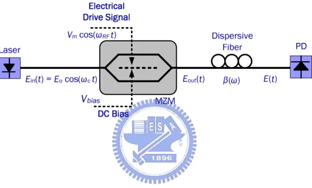
(27) Chapter 2 Theoretical Analysis of Millimeter-Wave Generation Using Double Sideband with Carrier Suppression. Since the MZM based on DSBCS modulation scheme is biased at the minimum transmission and operated at the nonlinear region, the MZM nonlinearity have a great influence on the performance of the mm-wave signal [1-2]. In addition, for a real MZM, a perfect 50/50 splitting ratio of the Y-splitter cannot be achieved, due to fabrication tolerances. Therefore, imperfect MZMs will have a finite extinction ratio (ER) and the mm-wave signals using DSBCS modulation will have finite OCSR. This will result in degrading the mm-wave signals. In this section, the impact of both the MZM nonlinearity and the imperfect MZM on the mm-wave signal performance will be theoretically analyzed. Optimum conditions for the mm-wave generation using DSBCS modulation will be discussed.. 2.1 Mm-Wave Generation Using Perfect MZM. The principle diagram of the optical mm-wave generation using DSBCS modulation scheme is illustrated in Fig. 2.1. For the perfect MZM, the power splitting ratio of two arms of the MZM is 0.5. The electrical field at the output of the single-arm MZM can be expressed as 10.
(28) cos where. and. cos. are the electric amplitude and angular frequency of the is the applied driving voltage, and Φ. input optical carrier,. optical carrier phase difference induced by MZM.. (1). is the. between the two arms of the. consisting of an electrical sinusoidal signal and a dc biased. voltage can be written as cos is the dc biased voltage,. where. (2) . and. are the amplitude and the. angular frequency of the electrical driving signal, respectively. The optical carrier phase difference induced by. can be expressed as. ΦV t where. cos. (3). is the half-wave voltage of the MZM. Therefore, the output. electrical field can be rewritten as cos. cos. 2. cos. cos. cos · cos sin · sin where voltage, and. cos. cos. cos cos. cos. 4. is a constant phase shift determined by the dc biased is the phase modulation index. Expanding (4) with. Bessel function leads to an expression for the electrical field as. 11.
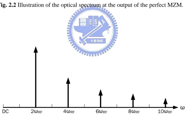
(29) ∞. cos. 2. cos. cos even. ∞. sin. 2. cos. cos. 5. odd. cos. cos. ∞. 2. cos 1. 2. cos ∞. sin. 2. cos. where . 2. cos. 1. 1. 6. is the Bessel function of the first kind of order n, and is equal to . √ 1. For DSBCS modulation, the bias voltage is set at have cos. 0 and sin. , and we. 1. Hence, the electrical field of the mm-wave. signal using DSBCS modulation can be written as ∞. ·. 2. cos cos. 2. 1 1. 7. All the even-order sidebands associated with the term sin are eliminated, and only the odd-order sidebands associated with the term cos. are kept, as. shown in Fig. 2.2. The amplitudes of the generated optical sidebands are proportional to those of the Bessel function associated with the phase 12.
(30) modulation index equal to. . With the amplitude of the electrical driving signal. , the maximum. is . As. ranges from 0 to , the Bessel. 1 decreases and increases with the order of Bessel. function. for. function and. , respectively.. ,. ,. , and. are 0.5668,. 0.0690, 0.0022, and 0.00003581, respectively. Therefore, the optical sidebands with the Bessel function higher than. can be ignored, and (7) can be. further simplified to cos. cos. cos. 3. cos. 3. cos. 5. cos. 5. 8. When optical DSBCS signals are transmitted over a single-mode fiber with dispersion, a phase shift to each optical sideband relative to optical carrier is induced [3]. The propagation constant of the dispersion fiber. can be. expressed as (9) where. is the derivative of the propagation constant. The effect of. high order fiber dispersion at 1550nm band is neglected. For carrier tones with central frequency at. , we have 1 2. 10. and 2 where. D. 11. is the speed in free space, D is the chromatic dispersion parameter. 13.
(31) and. is the frequency of the optical carrier. For a standard single-mode fiber,. D is 17 ps/(nm.km). Therefore, after transmission over a single-mode fiber of length z, the electrical field can be written as 1 2. cos. 1 2. cos cos. 3. 3. 9 2. cos. 3. 3. 9 2. cos. 5. 5. 25 2. cos. 5. 5. 25 2. After square-law detection using an ideal PD with responsitivity. 12. , the. photocurrent can be expressed as ·|. |. (13). The individual square term of (12) in (13) will generate the baseband signal, and the cross terms of (12) in (13) will generate the desired mm-wave signal and its harmonics distortion signals. These desired mm-wave terms are ·. 2 2. cos 4 cos 8. · cos 2. 2. · · cos 2. 14 2. cos 4. 2. 14. 14.
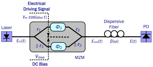
(32) ·. 2. 2. cos 4 · cos 4. ·. 4. 15. 2 · cos 6. ·. cos 12 6. 2 ·. cos 12. 16 · cos 8. cos 8. ·. 8. 10. · cos 10. 17 18 . The corresponding electrical spectrum of generated mm-wave signals is shown in Fig. 2.3. The original driving signal ( harmonics distortion signals (. , 3. ) and the odd terms of its. , 5. ….) are not observed, and the. even terms of its harmonics distortion signals (4. , 6. , 8. ….) can be. easily eliminated by using electrical filter. Therefore, the desired mm-wave signal (2. ) is attained by using ideal MZM based on DSBCS modulation. schemes.. 2.2 Mm-Wave Generation Using Imperfect MZM with Imperfect Power Splitting Ratio. For MZM with imperfect power splitting ratio, as shown in Fig.2.4, the electrical field at the output of the MZM can be written as: √. where. and. · 1. · exp. 1. ·√. · exp. · exp. (19). are the power splitting ratios of the first and second. Y-splitters in MZM, respectively, and. and. are optical carrier phase. shifts induced by the applied driving voltages in the upper and lower arms of. 15.
(33) MZM, respectively. Therefore, this imperfect structure allows the MZM to have a finite ER. The intrinsic MZM ER due to fabrication tolerances can be expressed as. If √. · 1. √. · 1. 1. ·√. √. · 1. 1. ·√. 1. · √ , we can rewrite the equation (19) as. · 1 1. 20. · exp. exp. ·. · 1. · exp · exp. · exp. 21. Hence, the modulation of the MZM with imperfect power splitting ratios can be viewed as the sum of a perfect MZM modulation and a phase modulator (PM) modulation which are represented in the first and second terms of equation (21), respectively. It is observed that the PM modulation can be 0.5, perfect MZMs, or. eliminated if. 1. . However, due to. fabrication tolerances, both conditions cannot be achieved. Thus, the PM modulation caused by the unbalanced power ratios of the impact MZM cannot be avoided. The electrical fields of the MZM and PM modulations can be rewritten as: _. · cos. _. · exp. 2. · exp. exp. 22. and. where 1. and. are 2. 23. · exp √. · 1. and. 1. ·√. √. ·. , respectively. Under the single-arm MZM condition, we have. 16.
(34) , and 2 where. and. can be expressed as cos 2. 2. cos and. are. 24. , respectively. The output electrical. field of the amplitude modulation can be rewritten as: · cos. _. · cos. 2. · cos. cos. cos · cos sin · sin. cos. cos cos. cos. ∞. cos ·. 2. cos even. ∞. sin. 2. cos. cos odd. cos. · cos. ∞. 2. cos 1. cos. 2. ∞. sin. 2. cos. cos. 2. 1. 1. For the phase modulation, the output electrical filed can be written as:. 17. 25.
(35) · exp. _. ·. exp. 2. · exp. cos. ·. ·. ·. ·. · sin ∞. ·. ·. · ∞. ∞. ·. · ∞ ∞. ·. · cos. 26. 2. ∞. For mm-wave signals based on DSBCS modulation with the bias voltage set at , cos. , we have. 0, and sin. 1. The output electrical. filed of the amplitude and phase modulations can be rewritten as ∞. 2. cos. _. 2. cos. 1. 1. 27. and ∞ _. ·. 1. · cos. 2. ∞. 28. It is reasonable that optical sidebands with the Bessel functions with the order higher than 5 can be ignored, and the electrical field at the output of the MZM with imperfect power splitting ratios can be simplified to. 18.
(36) _. _. sin cos cos 2. sin. cos. 3. cos. 3. 4. sin. cos. 5. cos. 5. sin. 2. sin. 4. 29. Figure 2.5 shows the optical spectrum of the mm-wave signals. The PM modulation due to imperfect MZMs not only affects the desired sideband 3. and odd-order sidebands also attributes to the carrier 4. ,. 5. and even-order sidebands. but 2. ,. . After transmission over dispersive fiber with , the electric field can be written as sin cos. 1⁄2. cos. 1⁄2. sin. 2. 2. 2. sin. 2. 2. 2. cos. 3. 3. 9⁄2. cos. 3. 3. 9⁄2. sin. 4. 4. 8. sin. 4. 4. 8. cos. 5. 5. 25⁄2. cos. 5. 5. 25⁄2. After square‐law detection using an ideal PD with responsitivity 19. 30. , the .
(37) photocurrents of the desired mm‐wave signal and its harmonics distortion signals can be expressed as ·. 2. sin. 1 2. 3 2 5 sin 2 7 sin 2. sin. sin. 9 2 31. · cos · 2. cos 2 cos 6. 2. cos 4 · cos 2. cos 8 ·. 2. 2. sin. 32. 9 2. 15 2 21 sin 2. sin. · cos 3 ·. sin. 3 2. 3. 33. 2. cos 8. 2. cos 12 cos 4. · cos 4 ·. 4. 34. 2. sin sin. · cos 5. 15 2. 25 2 sin. 5. 5 2 35. 20.
(38) ·. 2. cos 12. 2. cos 6 · cos 6. ·. 2. 6 sin. sin. 7 2. · cos 7. 36. 21 2 7. 37. · 2 · cos 8 ·. cos 8 8. 38. 2 · cos 9. sin 9. 9 2 39. · · cos 10. 10. 40. The phase modulation, caused by imperfect MZMs, not only contributes to the desired mm-wave signals and even-term distortion signals but also generates odd-term distortion signals. For the back-to-back (BTB) mm-wave signals, only the even-term signals are observed as shown in Fig. 2.6a. However, after transmission over dispersive fiber, the odd-term signals are also observed as shown in Fig. 2.6b. Although the undesired electrical distortion signals can be easily removed by electrical filter, the optical even-order sidebands, caused by phase modulation due to imperfect MZMs, can affect the ).. desired electrical mm-wave signal (. 2.3 Carrier-to-Distortion Ratio of MM-Wave Signal Using Perfect and Imperfect MZMs 21.
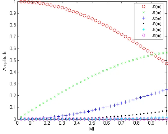
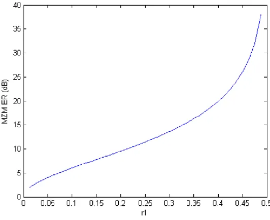
(39) A RoF lightwave system mainly consists of transmitters, fiber link, and receivers. The system performance is determined by the performance of those active and passive components. Due to the inherent nonlinearity of MZM, the optical undesired sidebands of the mm-wave signals based on DSBCS modulation scheme cannot be avoided even if perfect MZMs are utilized, as shown in Figs. 2.2 and 2.5. These undesired optical sidebands can degrade the performance of the desired electrical mm-wave signals, and the amplitudes of optical sidebands are related to the corresponding order of the Bessel function, , and. . The Bessel function is related to the electrical modulation ) for driving MZM as shown in Fig. 2.7. As MI. index (MI. decreases from 1 to 0, the 0th-order Bessel function increases and the Bessel function with the order of more than 1 decrease. Thus, the MZM nonlinearity can be reduced by decreasing MI but the OCSR of optical mm-wave signals will increase. The reductions of the MZM nonlinearity and OCSR can improve and degrade the performance of the optical mm-wave signals, respectively. and. are determined by. ideal second Y-splitter ( with. . As. and. . For simplicity, we assume an. 0.5). Figure 2.8 shows. decreases from 0.5 to 0,. and. and. varied. will decrease and. increases, respectively. Hence, the phase modulations play more and more important roles in optical mm-wave generations using imperfect MZMs as decreases. This will degrade the performance of optical mm-wave signals. In addition,. and. ER decreases when. determine the MZM ER as shown in Fig. 2.9. The MZM ranges from 0.5 to 1. For a commercial MZM, the ER. of more than 25dB, corresponding to. =0.444, is available. 22.
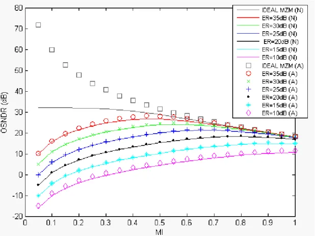
(40) The optimal operating condition for RoF systems constrained by nonlinearity is a balance between signal distortion and noise [4] as the MI for driving MZM decreases. However, for mm-wave signals using DSBCS modulation, the OCSR needs to be considered. The main noise sources of the optical link are relative intensity noise (RIN), thermal noise (TN), and shot noise (SN). The OSDR depends on the inherent nonlinearity of the MZM. Increasing the modulation index (MI) can provide more signal power to overcome noise issue, but it also increases the signal distortion. In addition, for the mm-wave signals using MZMs based on DSBCS modulation, decreasing the MI will contribute to less OCSR, resulting in degrading the performance of RoF systems. Hence, optical signal-to-noise ratio (OSNR) and optical signal-to-distortion ratio (OSDR) are used to evaluate the quality of the optical mm-wave signals using imperfect MZMs based on DSBCS modulation. The OSNR and OSDR can be expressed as [4] P Noise. P Noise. Noise P. P P. P. P. P. P. P. P. P. P. where P is the power of each optical sideband, and OSNDR is the combination of OSNR and OSDR. Figure 2.10 shows the OSNDR varied with. and. different MZM ERs. The commercial software, VPItransmissionMaker 5.0, is used to evaluate the numeric simulation. The RIN, TN, SN, and MZM nonlinearity are considered in the numeric stimulation, and only MZM nonlinearity is considered in the analytic stimulation. Both analytic and numeric stimulations show that the OSNDR increases first and then decreases as the MI for the MZM with ER of more than 15dB decreases from 1 to 0.1. 23.
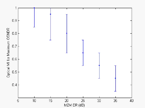
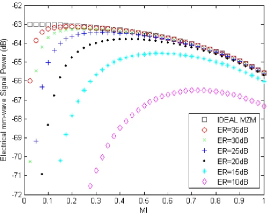
(41) The maximum OSNDR originates the reduction the MZM nonlinearity and the OCSR which can improve and degrade the OSNDR, respectively. Furthermore, the MZM ER can affect the maximum OSNDR. As the MZM ER ranges from 35dB to 15dB, the optimal MI for the maximum OSNDR will increase as shown in Fig. 2.11. However, when MZM ER is less than 15dB, the OCSR dominates the OSNDR. Thus, as the MI for the MZM with ER of less than 15dB decreases from 1 to 0.1, the OSNDR will decrease. Figure 2.12 shows the desired electrical mm-wave signals (. ) after PD. detection. The power of the optical mm-wave signals before PD is normalized to be 0dBm in the numeric stimulation, and RIN, TN, and SN are also included. The results are similar to the OSNDR. When 0<MI<1, the power of desired electrical mm-wave signals increases first and then decreases, and the optimal MI for the maximum. increases as the MZM ER decreases from 35dB to. 10dB as shown in Fig. 2.13. In summary, the MZM nonlinearity and the imperfect MZM with imperfect power splitting ratio have been demonstrated to have a great influence on the performance of the optical RF signals. With decreasing MI for driving imperfect MZMs, the reduction of nonlinearity and OCSR can improve and degrade the mm-wave signal performance, respectively. Hence, there is an optimal MI for the RF signals using DSBCS modulation. In conventional DSBCS modulation scheme, the DD-MZM is utilized to get full MI (MI=1) and high OCSR. According to simulation results, the optimal MI for imperfect MZMs with ER of more than 20dB is less than 0.7, as shown in Fig. 2.13. Therefore, only SD-MZM is needed to realize DSBCS modulation, which is more compact and cost-effective. Moreover, the performance of the mm-wave signals can be improved. 24.
(42) References [1] W. H. Chen, and W. I. Way, “Multichannel Single-Sideband SCM/DWDM Transmission System,” J. Lightwave Technol., vol. 22, no. 7, pp. 1697-1693, July 2004. [2] C. Wu, and X. Zhang, “Impact of Nonlinear Distortion in Radio Over Fiber Systems with Single-Sideband and Tandem Single-Sideband Subcarrier Modulations,” J. Lightwave Technol., vol. 24, no. 5, pp. 2076-2090, May 2006. [3] L. Cheng, S. Aditya, Z. Li, and A. Nirmalathas, “Generalized Analysis of Subcarrier. Multiplexing. in. Dispersive. Fiber-Optic. Links. Using. Mach-Zehnder External Modulator,” J. Lightwave Technol., vol. 24, no. 6, pp. 2296-2304, June 2006. [4] T. E. Darcie, “Subcarrier Multiplexing for Lightwave Networks and Video Distribution,” IEEE J. on Selected Area in Communication, vol. 8, no.7, pp. 1240-1248, 1900.. 25.
(43) Fig. 2.1 The principle diagram of the optical mm-wave generation using perfect MZM based on DSBCS modulation.. 26.
(44) Fig. 2.2 Illustration of the optical spectrum at the output of the perfect MZM.. Fig. 2.3 Illustration of the electrical spectrum of mm-wave signals using perfect MZM after square-law PD detection.. 27.
(45) Fig. 2.4 The principle diagram of the optical mm-wave generation using imperfect MZM based on DSBCS modulation.. Fig. 2.5 Illustration of the optical spectrum at the output of the imperfect MZM.. 28.
(46) (a). (b). Fig. 2.6 Illustration of the electrical spectrum of generated mm-wave signals using imperfect MZM after square-law PD detection. (A) BTB mm-wave signals. (b) Mm-wave signals after transmission over dispersion fiber.. 29.
(47) Fig. 2.7 Amplitude of the Bessel function varied with MI.. 30.
(48) Fig. 2.8. and. varied with. .. 31.
(49) Fig. 2.9 MZM ER varied with. .. 32.
(50) Fig. 2.10 OSNDR of the optical mm-wave signals varied with MI. A: Analytic stimulation, N: Numeric stimulation.. 33.
(51) Fig. 2.11 Optimal MI for maximum OSNDR of the optical mm-wave signals. The solid spot indicates the optimal MI for each MZM ER. The range of optimal MI comes from 1-dB tolerance of the maximum OSNDR.. 34.
(52) Fig. 2.12 Desired electrical mm-wave signals varied with MI after PD detection.. 35.
(53) Fig. 2.13 Optimal MI for the electrical mm-wave signal generation. The solid spot indicates the optimal MI for each MZM ER. The range of optimal MI comes from 1-dB tolerance of the maximum power of the electrical mm-wave signal.. 36.
(54) Chapter 3 Optical Convergence Access Network Providing Wired-Line and Wireless Signals. Recently, the optical-wireless networks offering both broadband wireless and wired services have attracted a lot of attention [1-5]. This architecture can provide both advantages form both sides: mobility and point-to-multi-points access technology from ultra wideband wireless network, and high bandwidth and highly reliable connection from optical access network. The key issue is to generate and transmit wireless and wired-line signals simultaneously. In this chapter, we propose and experimentally demonstrate dual-service optical-wireless access network providing wireless and wired-line signals and hybrid access network integrating RoF and FTTH systems. Moreover, optimum conditions for the mm-wave generation using DSBCS modulation will be experimentally investigated.. 3.1 Dual-Service Optical-Wireless Access Network. In this section, we propose a novel optical-wireless network offering a simple method to simultaneously generate the RF and BB signals using only one MZM. The DSBCS modulation scheme using external MZM is utilized to generate the RF signals. Since the MZM is operated at the nonlinear region, we 37.
(55) study the relationship between the RF modulation index (MI-RF=Vp-p/2Vπ) for driving DD-MZM and the receiver sensitivity to investigate the impact of the MZM nonlinearity on the performance of BB and RF signals. When MI is set to 0.43, there is 1dB improvement for the receiver sensitivity of the RF signal based on DSBCS modulation scheme and on power penalty for BB signals is observed. Based on this result, only one SD-MZM is needed to generate the mm-wave based on DSBCS modulation scheme, which is more compact and cost-effective. We also prove that BB signals are more robust to the fiber nonlinearity than the RF signals.. 3.1.1 Experimental Setup Figure 3.1 shows the experimental setup used for the simultaneous generation and transmission of optical RF and BB signals based on DSBCS modulation scheme. The continuous wave (CW) laser is generated by a distributed feedback laser, and the emission wavelength is 1540 nm. The BB signal is 622 Mb/s pseudo random bit sequence (PRBS) signal with a word length of 231-1 and up-converted with the 5 GHz clock as shown in inset (i) of Fig. 3.1. The up-converted signal is amplified to maximum peak-to-peak voltage (Vp-p) of 7 volt, limited by the commercial RF amplifier (Picosecond 5865). The CW laser is modulated via external SD-MZM or DD-MZM with half-wave voltage (Vπ) of 5 volt. In order to realize DSBCS modulation, the MZM is biased at the minimum transmission point. The repetition frequency of the generated optical microwave is 10 GHz. The optical microwave and spectrum of RF signals are shown in insets (ii) and (iii) of Fig. 3.1, respectively. The generated RF signal is amplified by erbium-doped fiber amplifier (EDFA) and then filtered by a tunable optical filter with a bandwidth of 0.4 nm. After 38.
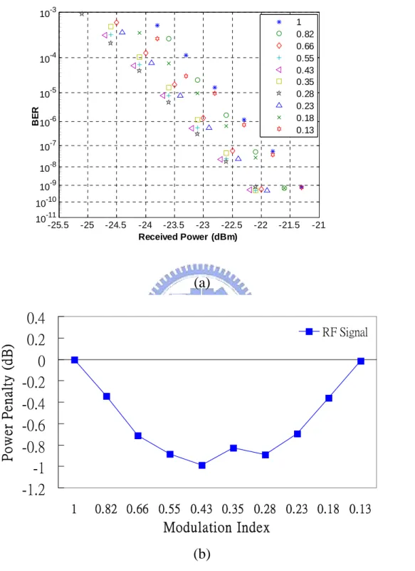
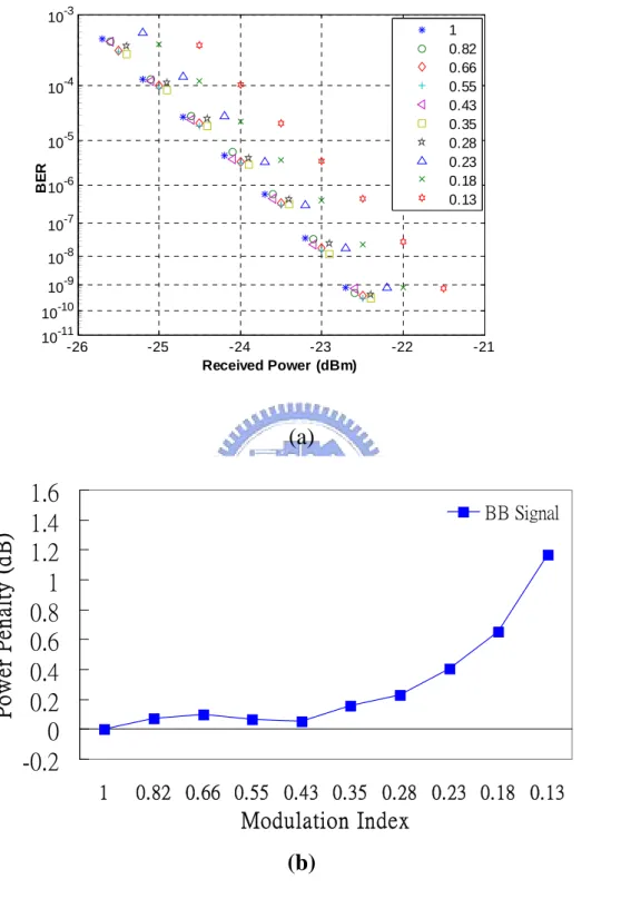
(56) transmitted over SSMF, the transmitted optical microwave signal is converted into an electrical microwave signal by a PD with a 3 dB bandwidth of 38 GHz, and the converted electrical signal is amplified by an electrical amplifier. In the BB path, a low-pass filter with a 3 dB bandwidth of 622 MHz is inserted to reject the undesired RF components. In the other path, the microwave signal is down-converted (DC) by a mixer with a 10 GHz clock, and then passes through a low-pass filter with a 3 dB bandwidth of 622 MHz. The eye diagrams of the DC and BB signals are shown in insets (iv) and (v) of Fig. 3.1, respectively. Both the DC and BB signals are tested by a bit-error-ratio (BER) tester. We set the fiber lengths to be 25, 50, 75 and 100 km.. 3.1.2 Experimental Results and Discussion Figure 3.2 and 3.3 show the variations of the receiver sensitivities and power penalties of the BB and DC signals with MI-RF, respectively. For the DC signal, the receiver sensitivity increases first and then decreases when MI-RF ranges from 1 to 0.13, and the best sensitivity is at MI-RF equal to 0.43. For the BB signal, no receiver sensitivity penalty is observed when MI-RF decrease from 1 to 0.43. As MI-RF changes from 0.43 to 0.28, the sensitivity degradation is only 0.3 dB at BER of 10-9. The MZM nonlinearity and OCSR are closely related to MI-RF. As MI-RF for MZM decreases, the MZM nonlinearity and OCSR decrease. The reduction of the MZM nonlinearity makes the duty cycle of optical microwaves closer to 0.5 as shown in Fig. 3.4. At the same optical power, optical microwaves smaller duty cycle have higher peak power, resulting in better receiver sensitivity of the DC signal. However, low OCSR means that the RF component of optical power is relative low and the dc component of optical 39.
(57) power at the center wavelength is relative high as shown in Fig. 3.5. This incurs worse receiver sensitivity of the DC signal. Therefore, there is a trade-off for the receiver sensitivity of the DC signal between the MZM nonlinearity and OCSR when we decrease MI-RF. The result is in accordance with the theoretical simulation in previous chapter. When the optimal MI-RF is 0.43, the receiver sensitivities of the BB and DC signals at BER of 10-9 are -22.6 dBm and -22.7 dBm, respectively. The receiver sensitivity of the DC signal has 1 dB improvement when MI-RF changes from 1 to 0.43. After optical microwaves with optical power of 0 dBm, using the optimal MI-RF equal to 0.43, are transmitted over 25 km, 50 km, and 75 km SSMF, the power penalty for the receiver sensitivities of the BB and DC signals at BER of 10-9 is less than 0.2dB as shown in Fig. 3.6. Based on the result of DSBCS modulation using one DD-MZM, we can generate DSBCS microwaves using only one SD-MZM with MI-RF equal to 0.43. The Vπ of the SD-MZM at 5GHz is 5 volt, and the Vp-p for the MI-RF of 0.43 is 4.3 volt. Figure 3.7 shows the receiver sensitivities and power penalties of the BB and DC signals with optical power of 0dBm after they are transmitted over 25 km, 50 km and 75 km SSMF. The power penalties for both the BB and DC signals at BER of 10-9 are less than 0.3 dB. We also study the impact of fiber nonlinearity on optical microwave signals. Figure 3.7 shows the power penalty of the receiver sensitivity at BER of 10-9 under various optical microwave powers. The BB signal shows better robustness to the impairments of fiber nonlinearity effects, and only 0.3 dB sensitivity penalty is observed when the optical microwave power increases from 0 to 10 dBm. However, the sensitivity of the DC signal degrades more severely when the optical microwave power increases to 10 dBm. The reason is 40.
(58) that the effect of both fiber nonlinearity and dispersion changes the duty cycle of optical microwaves as shown in insets (i)-(v) of Fig. 3.8. That is why the DC signal transmitted over 75 km SSMF has the worst receiver sensitivity. Therefore, we can conclude that the power penalty for both the receiver sensitivities of the BB and DC signals using only one SD-MZM based DSBCS scheme is less than 1.4 dB after transmitted over 100 km SSMF when the optical power ranges from 0 to 10 dBm. In summary, this section presents a simultaneous generation of BB and RF signals based on DCBCS modulation scheme using only one MZM. The optimal MI-RF level for driving DD-MZM is 0.43 with 1 dB sensitivity improvement for DC signals, and there is no receiver sensitivity penalty after transmission over 75 km SSMF. Based on the optimal MI of 0.43, we can generate DSBCS microwaves using only one single-electrode MZM, which is more compact and cost-effective. The receiver sensitivity penalty is less than 0.3 dB after transmitted over 75 km SSMF. We also confirm that BB signals have better robustness to the impairment of fiber nonlinearity than RF signals.. 3.2 Hybrid Optical Access Network. In this section, we propose a hybrid optical access network integrating RoF and FTTH systems. This proposed system provides the simultaneous modulation and transmission of a BB signal and a RF signal on a single wavelength over a single fiber. The BB and RF signals are independently modulated and transmitted at the optical carrier and subcarrier, respectively. In the proposed system, unlike [4-5], the RF signal does not suffer periodic 41.
(59) performance fading when it is transmitted over a SSMF. The power penalties of both BB and RF signals are less than 0.2dB after transmission over 50km SSMF, revealing the feasibility of the system.. 3.2.1 Hybrid Optical Access Network Architecture Figure 3.9 schematically depicts the hybrid optical access network system. An external integrated modulator using x-cut LiNbO3 [6-7], consisting of three SD-MZM, is the key to generating RF and BB signals simultaneously. Two sub-MZMs (MZ-a and MZ-b) are embedded in each arm of the main modulator (MZ-c). Both DSB and DSBCS modulation schemes are used to generate the RF signals at MZ-a. The optical spectrums of RF signals are shown in inset (i) of Fig.3.9. The BB signal is generated at MZ-b and modulated at the optical carrier, as shown in the inset (ii) of Fig.3.9. The optical RF signal and BB signal are combined at MZ-c biased at the maximum transmission point. The inset (iii) of Fig.3.9 shows the optical spectrum of the hybrid signal. At a remote node, a optical filter is utilized to separate these two signals, as shown in inset (iv) and (v) of Fig.3.9, and each signal is transmitted to the corresponding application.. 3.2.2 Experimental Setup Figure 3.10 shows the experimental setup for hybrid signal generation and transmission using one external integrated modulator. The continuous wave (CW) laser is generated by a tunable laser, and the lasing wavelength is 1554.94nm. The RF signal is a 622Mb/s PRBS signal with a word length of 231-1 and up-converted with the 10 GHz clock as shown in inset (i) of Fig.3.10. The up-converted RF signal is amplified to maximum Vp-p of 7V, limited by the 42.
(60) RF amplifier. The optical RF signal is generated via MZ-a with Vπ of 5.8V. The MZ-a is biased at the minimum and quadrature transmission point to realize DSBCS and DSB modulation, respectively. The repetition frequencies of the generated optical microwave using DSBCS and DSB modulations are 20GHz and 10GHz, respectively. The generated optical microwave is shown in inset (ii) of Fig. 3.10. The BB signal is a 1.25Gb/s PRBS signal with a word length of 231-1; it is sent into MZ-b with Vπ of 5.6V. The eye diagram of the generated optical BB signal is shown in inset (iii) of Fig. 3.10. The optical RF and BB signals are combined at MZ-c with Vπ of 6.9V biased at the maximum transmission point. The hybrid optical signals are amplified by an EDFA to compensate for the loss of the external modulator, yielding a power of 0dBm before transmission over 50km SSMF. Following transmission over 50km SSMF, the hybrid signals are preamplified by EDFA and then filtered by a tunable optical filter with a bandwidth of 0.4nm. At the remote node, the fiber grating with a 3dB bandwidth of 4GHz is used to separate these two signals, as shown in inset (iv) and (v) of Fig. 3.10, and each signal is sent to the corresponding application. Both optical signals are individually detected by a PIN PD. For FTTH applications, the electrical BB signal is filtered by a electrical filter with a 3dB bandwidth of 1.25GHz. For wireless applications, the electrical RF signal is down-converted by a mixer with a 20GHz clock before passing through a low-pass filter with a 3dB bandwidth of 622MHz. The eye diagrams of BB and RF signals are shown in inset (vi) and (vii) of Fig. 3.10, respectively. Both RF and BB signals are tested by a BER tester and the receiver sensitivities are measured before EDFA pre-amplification. The fiber lengths are set at 25 and 50km.. 43.
(61) 3.2.3 Experimental Results and Discussion Since the BB and RF signals are generated at different sub-MZs, these two signals can be optimized individually. Especially, the RF signal performance is strongly related to MZM nonlinearity. To optimize the RF signal performance, the RF modulation index MI-RF= Vp-p/2Vπ and MI-RF= Vp-p/Vπ for driving MZ-a based on DSBCS and DSB modulation schemes decreases to reduce the MZM nonlinearity, respectively, and no BB signals are sent to MZ-b biased at the minimum transmission point. Figure 3.11 shows the variation of the receiver sensitivity of the RF signal using DSBCS modulation with different MI-RF. The RF receiver sensitivity initially improves and then declines as the MI-RF decreases from 0.6 to 0.1 When MI-RF is 0.48, the RF signals exhibit the best sensitivity. The optimal MI-RF for RF signals using DSBCS modulation originates from the trade-off between the MZM nonlinearity and the OCSR for the RF receiver sensitivity when MI-RF is decreased. This has been theoretically and experimentally in chapter 2 and section 3.1. For RF signals using DSB modulation, the result is different as shown in Fig.3.12. As MI-RF decreases, not only MZM nonlinearity decreases but also optical modulation index (OMI) of the RF signals decreases. Reduction of MZM nonlinearity can improve RF sensitivity, but reduction of OMI will degrade RF sensitivity. However, the OMI dominates the RF performance as shown in Fig. 3.13. Therefore, As MI-RF decreases, the RF sensitivity degrades. The optimal MI-RF for RF signals using DSB modulation is 1. After finding the optimal driving condition for MZ-a, there are two ways. 44.
(62) to control the optical power ratios of the RF and BB signals to the hybrid signals. One is to control the splitting ratio before MA-a and MZ-b. However, the optical power ratios of the RF and BB signals to the hybrid signals is not adjustable after the integrated MZM is fabricated. Therefore, we propose the other method. The optimal MI-RF for driving MZ-a is fixed at 0.48, and then the BB signal is sent to MZ-b. The BB modulation index (MI-BB) for driving MZ-b decreases from 1 to 0.18. The bias point of MZ-b is adjusted to maximize the ER of the BB signal as MI-BB varies from 1 to 0.18. As MI-BB decreases, the optical power ratios of the RF and BB signals to the hybrid signals increase and decrease, respectively. Hence, the BB sensitivity increases and the RF sensitivity decreases as MI-BB ranges from 1 to 0.18, as shown in Fig. 3.14. For RF signals using DSBCS modulation, the same sensitivities of the RF and BB signals can be achieved as the MI-BB is 0.27. However, for RF signals using DSB modulation, the same sensitivities of the RF and BB signals cannot be achieved, and even error floor is observed when MI-BB is 0.27. Therefore, the DSBCS modulation is the best choice for the RF signal generation in the proposed system. In this study, we did not consider the RF signals transmitted over air. For the real situation, the requirements of the RF and BB signals are different. The optical power ratios of the RF and BB signals to the hybrid signals should be controlled to meet the different requirements. Therefore, the interference between BB and RF signals is needed to concern when we control the optical power ratios of the RF and BB signals to the hybrid signals [4-5]. The RF sensitivity is measured after the fiber grating as shown in Fig.3.15. Figure 3.16 shows that the RF sensitivity deviation is less than 0.3dB as optimal MI-RF is fixed at o.48 and MI-BB ranges from 1 to 0.18. Hence, unlike in other works 45.
(63) [4-5], various MI-BBs for driving MZ-b cannot influence the RF signal performance when optimal MI-RFs for driving MZ-a are maintained. Therefore, our proposed system can meet different RF and BB signal performance requirements without fading RF and BB signals. Under optimal conditions using DSBCS modulation for RF signals to drive MZ-a and MZ-b, the receiver sensitivities of the RF and BB signals are -37.2dBm and -36.8dBm at BER of 10-9, respectively. Then the optical hybrid signals at an optical power of 0dBm are transmitted over 25km and 50km SSMF. Figure 3.17a plots the BER curves of the RF and BB signals. The power penalties of both signals at a BER of 10-9 are less than 0.2dB, as shown in Fig.3.17b. In conclusion, this section experimentally demonstrates the simultaneous modulation and transmission of FTTH BB and RoF RF signals using one external integrated modulator. The generated hybrid signals do not suffer from periodic performance fading problem caused by fiber dispersion. The receiver sensitivity penalties of both RF and BB signals are less than 0.2dB after transmission over 50km SSMF. The results reveal that the proposed system has great potential for use in future multi-service access networks.. References [1] G. K. Chang, J. Yu, Z. Jia and J. Yu, “Novel optical-wireless access network architecture for simultaneously providing broadband wireless and wired services,” 2006 Optical Fiber Communication Conference (OFC 2006), OFM1, Anaheim, California, March 05-10, 2006. [2] J. Yu, Z. Jia, L. Yi, G. K. Chang, and T. Wang, “Optical millimeter-wave 46.
(64) generation or up-conversion using external modulator,” IEEE Photon. Technol. Lett., vol. 18, pp. 265-267, 2006. [3] A. Martinez, V. Polo, and J. Marti, “Simultaneous baseband and RF optical modulation scheme for feeding wireless and wireline heterogeneous access network,” IEEE Trans. Microwave theory and Technol., vol. 49, pp. 2018-2024, 2001. [4] T. Kamisaka, T. Kuri, K. Kitayama, “Simultaneous modulation and fiber-optic transmission of 10Gb/s baseband and 60GHz band radio signals on a single wavelength,” IEEE Trans. Microwave theory and Technol., vol. 49, pp. 2013-2017, 2001. [5] K. Ikeda, T. Kuri, and K. Kitayama, “Simultaneous three band modulation and fiber-optic transmission of 2.5Gb/s baseband, microwave-, and 60GHz band signals on a single wavelength,” IEEE J. Lightwave Technol., vol. 21, pp. 3194-3202, 2003. [6] T. Kawanishi, K. Higuma, T. Fujita, S. Mori, S. Oikawa, J. Ichikawa , T. Sakamoto and M. Izutsu , “40Gbit/s Versatile LiNbO3 Lightwave Modulator ,” European Conference on Optical Communication (ECOC 2005), Glasgow, Scotland, Paper No.: Th2.2.5, 2005. [7] T.. Sakamoto,. T.. Kawanishi,. and. M.. Izutsu,. “Continuous-Phase. Frequency-Shift Keying With External Modulation,” IEEE Journal OF Selected Topics in Quantum Electronics, Vol. 12, no. 4, pp. 589-595, July/August 2006.. 47.
(65) 0V. Baseband 622Mb/s. 5GHz Clock Time (2ns/div). PC. MZ MOD. EDFA BW=0.4 nm Optical OBPF Attenuator. Time (0.5ns/div). SSMF O/E. 10GHz Clock. 622MHz LPF 622MHz. Time (2ns/div). BERT Resolution 0.01nm. Time (0.5ns/div). Down-converted Signal. LPF BERT Baseband Signal. Fig. 3.1 Experimental setup for the generation and transmission of optical RF and BB signals based on DSBCS modulation scheme using one MZM.. 48.
(66) 10. 10. BER. 10 10 10 10 10 10 10. -3. 1 0.82 0.66 0.55 0.43 0.35 0.28 0.23 0.18 0.13. -4. -5. -6 -7 -8 -9. -10 -11. -25.5. -25. -24.5. -24 -23.5 -23 -22.5 Received Power (dBm). -22. -21.5. -21. Power Penalty (dB). (a). 0.4 0.2 0 -0.2 -0.4 -0.6 -0.8 -1 -1.2. RF Signal. 1. 0.82 0.66 0.55 0.43 0.35 0.28 0.23 0.18 0.13. Modulation Index. (b) Fig. 3.2 BER curves (a) and power penalties at BER of 10-9 (b) of DC signals for different MI-RF.. 49.
(67) 10. 10. BER. 10 10 10 10 10 10 10. -3. 1 0.82 0.66 0.55 0.43 0.35 0.28 0.23 0.18 0.13. -4. -5. -6 -7 -8 -9. -10 -11. -26. -25. -24 -23 Received Power (dBm). -22. -21. Power Penalty (dB). (a). 1.6 1.4 1.2 1 0.8 0.6 0.4 0.2 0 -0.2. BB Signal. 1. 0.82 0.66 0.55 0.43 0.35 0.28 0.23 0.18 0.13. Modulation Index. (b) Fig. 3.3 BER curves (a) and power penalties at BER of 10-9 (b) of BB signals for different MI-RF.. 50.
(68) (a). (b). (d). (c). (e). Fig. 3.4 Duty cycles of optical microwaves based on DSBCS modulation. The optical microwave power is 1dBm. The optical power scale is 0.8 mW/div and the time scale is 20 ps/div. The MI-RF is set at (a) 1 (b) 0.66 (c) 0.43 (d) 0.28 (e) 0.18.. 51.
(69) (a). (b). (d). (c). (f). Fig. 3.5 The OCSR of optical microwaves based on DSBCS modulation. The resolution is 0.01nm. The MI-RF is set at (a) 1 (b) 0.66 (c) 0.43 (d) 0.28 (e) 0.18. 52.
(70) Power Penalty (dB). (a) 1 0.8 0.6 0.4 0.2 0 -0.2 -0.4 -0.6 -0.8 -1. RF Signal BB Signal. BTB. 25km. 50km. 75km. (b). Fig. 3.6 BER curves (a) and power penalties at BER of 10-9 (b) using one DD-MZM with MI-RF of 0.43 after transmission over 25 km, 50 km and 75 km SSMF.. 53.
(71) Power Penalty (dB). (a) 1 0.8 0.6 0.4 0.2 0 -0.2 -0.4 -0.6 -0.8 -1. RF Signal BB Signal. BTB. 25km. 50km. 75km. (b). Fig. 3.7 BER curves (a) and power penalties at BER of 10-9 (b) using one SD-MZM with MI-RF of 0.43 after transmitted over 25 km, 50 km, and 75 km SSMF. 54.
(72) Optical Power Penalty(dB). 1.5. Down-converted 10dBm Down-converted 6dbm Down-converted 3dbm Down-converted 0dbm Baseband 10dBm Baseband 6dBm Baseband 3dBm Baseband 0dBm. 1. 0.5. (iv) (v). 0. -0.5. (i). (ii). (iii). -1. -1.5. BTB. 25km. 50km. 75km. 100km. Fig. 3.8 Fiber nonlinearity impairment of the receiver sensitivity. The MI-RF for SD-MZM is 0.43. The optical power scale is 0.8 mW/div and the time scale is 20 ps/div. (i)10 dBm, BTB (ii)10 dBm, 25 km (iii)10 dBm, 50 km (iv)10 dBm, 75 km (v)10 dBm, 100 km. 55.
(73) Fig. 3.9 Schematic diagram of the hybrid optical access network.. 56.
(74) DSB modulation. (II) DSBCS modulation. (I). 0V. RF 622Mb/s. 10GHz Clock. Integrated Modulator. 1 ns/ div. 1ns/div. MZ-a. PC. MZ-b. Tunable Laser. EDFA. MZ-c. Baseband 1.25Gb/s (vi). Optical Attenuator. (vi). 200ps/div 1.25GHz Baseband BERT Signal. RF Signal. 0 dBm. 200ps/div O/E. 200ps/div. EDFA. LPF Fiber grating. LPF O/E. 20 GHz Clock. (vii). Optical Attenuator Optical power meter. (iv). 622MHz BERT. SSMF. Sensitivity Measurement. BW=0.4 nm OBPF. Electrical. (v). Optical 1ns/div. 500ps/div. Fig. 3.10 Experimental setup for RF and BB signal generation and transmission using one external integrated modulator.. 57.
(75) 10. 10. BER. 10 10 10 10 10 10 10. -3. MI-RF=0.6 MI-RF=0.53 MI-RF=0.48 MI-RF=0.4 MI-RF=0.33 MI-RF=0.26 MI-RF=0.17 MI-RF=0.1. -4. -5. -6 -7 -8 -9. -10 -11. -44. -42. -40 -38 -36 -34 Received Power (dBm). -32. -30. (a). Power Penalty (dB). 10. RF Signal. 8 6 4 2 0 -2 0.6. 0.53. 0.48. 0.4. 0.33. 0.26. 0.17. 0.1. Modulation Index. (b) Fig. 3.11 BER curves (a) and power penalties at BER of 10-9 (b) of RF signals using DSBCS modulation for MI-RF from 0.6 to 0.1.. 58.
(76) 10. 10. BER. 10 10 10 10 10 10 10. -3. MI=0.96 MI=0.8 MI=0.65 MI=0.52 MI=0.42 MI=0.25 MI=0.16. -4. -5. -6 -7 -8 -9. -10 -11. -40. -35. -30. -25 -20 -15 -10 Received Power (dBm). -5. 0. 5. (a). Power Penalty (dB). 35. RF Signal. 30 25 20 15 10 5 0 1. 0.8. 0.65. 0.52. 0.42. 0.25. 0.16. Modulation Index (b) Fig. 3.12 BER curves (a) and power penalties at BER of 10-9 (b) of RF signals using DSB modulation for MI-RF from 1 to 0.16. 59.
(77) (a). (b). (e). (c). (f). (d). (g). Fig. 3.13 Eye diagrams of RF signals using DSB modulation for MI-RF from 1 to 0.16. (a) MI-RF=1 (b) MI-RF=0.8 (c) MI-RF=0.65 (d) MI-RF=0.52 (e) MI-RF=0.42 (f) MI-RF=0.25 (g) MI-RF=0.16. (Power scale: 270μ W/div, Time scale: 20ps/div). 60.
(78) BER. 10. 10. -4. 10. -5. 10. -6. 10 10 10. RF(MI-BB=1) BB(MI-BB=1) RF(MI-BB=0.8) BB(MI-BB=0.8) RF(MI-BB=0.63) BB(MI-BB=0.63) RF(MI-BB=0.45) BB(MI-BB=0.45) RF(MI-BB=0.27) BB(MI-BB=0.27) RF(MI-BB=0.18) BB(MI-BB=0.18). -3. -7 -8 -9. 10. -10. 10. -11. -45. -40. -35 -30 Received Power (dBm). -25. (a) 10. 10. BER. 10 10. -3. -4. -5. -6. 10. -7. 10. -8. 10 10 10. RF(MI-BB=1) BB(MI-BB=1) RF(MI-BB=0.63) BB(MI-BB=0.63) RF(MI-BB=0.36) BB(MI-BB=0.36) RF(MI-BB=0.27) BB(MI-BB=0.27). -9. -10 -11. -45. -40. -35 -30 -25 -20 Received Power (dBm). -15. -10. (b) Fig. 3.14 BER curves of BB and RF signals for MI-BB from 1 to 0.18. MI-RF is fixed at 0.48. 61.
(79) LD EDFA. OBPF. Fiber grating Optical power meter. Optical Attenuator. Fig. 3.15 Experimental setup to study the interference between BB and RF signals.. 62.
數據
+7
相關文件
Promote project learning, mathematical modeling, and problem-based learning to strengthen the ability to integrate and apply knowledge and skills, and make. calculated
Now, nearly all of the current flows through wire S since it has a much lower resistance than the light bulb. The light bulb does not glow because the current flowing through it
Simulation conditions are introduced first and various characteristics in three defect designs, such as single mode laser wavelength shift and laser mode change, are analyzed.
• All provisions of facilities such as trunks, conduits, cables, LAN ports and power points, shall be considered as fixture of the School venues and shall become the property of
電機工程學系暨研究所( EE ) 光電工程學研究所(GIPO) 電信工程學研究所(GICE) 電子工程學研究所(GIEE) 資訊工程學系暨研究所(CS IE )
- Attempted to distribute infringing copies of copyright works to such extent as to affect prejudicially the rights of the copyright
This design the quadrature voltage-controlled oscillator and measure center frequency, output power, phase noise and output waveform, these four parameters. In four parameters
This research project is to analyze and research a specific laser configuration to obtain complete knowledge、technologies and experiences to transfer to the project initiator for
