國 立 交 通 大 學
電子工程學系 電子研究所
碩士論文
含氮氧化層應用於二氧化鉿儲存層快閃記憶體資料儲存時
間之改善
Oxynitride Layer Applied to Flash Memory using HfO
2as
Charge Trapping Layer for Improved Data Retention
研 究 生:鄭 元 愷
指導教授:羅 正 忠 博士
新穎含氮氧化層應用於二氧化鉿儲存層快閃記憶體之研究
Study on Novel Oxynitride Layer Applied to Flash Memory
using HfO
2as Charge Trapping Layer
研究生:鄭元愷 Student:Yuan-Kai, Zheng
指導教授:羅正忠博士 Advisor:Dr. Jen-Chung Lou
國立交通大學
電子工程學系 電子研究所
碩士論文
A Thesis
Submitted to Department of Electronics Engineering & Institute of Electronics College of Electrical and Computer Engineering
National Chiao Tung University In Partial Fulfillment of the Requirements
For the Degree of Master In
Electronics Engineering August 2008
摘要
含氮氧化層應用於二氧化鉿儲存層快閃記憶體資料儲存時間之改善
研究生:鄭元愷 指導教授:羅正忠 博士 國立交通大學 電子工程學系 電子研究所 摘要 本論文著重於如何改善快閃記憶體的可靠度問題,如儲存資料的保留時間 (retention)。傳統快閃記憶體的穿隧氧化層(tunnel oxide)採用乾氧成長二氧化矽(dry SiO2)。但當氧化層厚度小於7奈米時,氧化層中的缺陷很容易產生漏電流路徑,使得被 儲存在捕捉層(trapping layer)的電荷透過穿隧氧化層中的漏電路徑而流失,而造成資料 的誤判。因此本論文採用新的含氮氧化層的技術取代傳統的乾氧化層,藉由減少界面狀 態及層內的缺陷(interface states and bulk defects)來提升快閃記憶體的可靠度特性。而本 論文所提出的新含氮氧化層製程技術是符合互補式金氧半(CMOS)場效電晶體的標準 製程,因此對於目前工業界的生產技術是可行的改善方法。傳統的非揮發性記憶體是採用複晶矽浮停閘(Poly-Silicon Floating Gate)作為電荷載子儲 存的單元,而電荷在複晶矽中是均勻分佈的,因此若出現漏電路徑,儲存的電荷將會全 部流失。而電荷在氮化矽中是屬於離散式的分佈,因此SONOS的結構被提出而取代傳統 的複晶矽浮停閘。但為了提升快閃記憶體的寫入速度及降低操作電壓,本論文採用二氧 化鉿層作為電荷捕捉層,稱之為SOHOS結構。我們製作SOHOS憶體元件,最後再做完 整的電性測量分析。 由本論文的結果,可知道新的含氮氧化層可完全運用在快閃記憶體元件上,並且可 以透過提升穿隧氧化層的品質,而達到改善快閃記憶體的可靠度問題。因此對於未來元 件的尺寸微縮及改善特性,新穎的含氮氧化層製程技術是很有潛力及備受期待的。
ABSTRACT
Oxynitride Layer Applied to Flash Memory Using HfO
2as Charge
Trapping Layer for Improved Data Retention
Student:Yuan-Kai, Zheng Advisor:Dr. Jen-Chung Lou
Department of Electronics Engineering & Institute of Electronics College of Electrical and Computer Engineering
National Chiao-Tung University
Abstract
This study focuses on how to improve the reliabilities of Flash memory, including the data retention. The tunnel oxide of conventional Flash memory is dry SiO2 layer. When the thickness of tunnel oxide layer is thinner than 7nm, the defects of tunnel oxide will form the leakage path easily. The trapped charges in trapping layer leak out through the leakage path and let we read the wrong data information. Therefore, the novel oxynitride process proposed in this study can replace the conventional dry oxide layer and improve the reliabilities of Flash memory by reducing the interface states and bulk defects. Moreover, the novel oxynitride process is compatible with standard CMOS process today and it is practicable
improvement in industry manufacturing.
The charge storage unit of conventional nonvolatile memory is Poly-Silicon Floating Gate and the charges in poly-Si distribute uniformly. If there were leakage path, the trapping charges would all lead out. While the charges distribute discretely in Si3N4 layer, the SONOS structure was proposed and replaced the conventional poly-Si floating gate. To promote the program speed and lower the operating voltage, the HfO2 layer worked as trapping layer in this study and was called SOHOS structure. We found the better PDA conditions of HfO2 film applied the optimum condition in integrated Flash memory devices. Finally, the complete electrical measurements and analysis were carried out.
From the result of this study, we confirm that the novel oxynitride process can be applied in Flash memory cells fully. The oxynitride can promote the reliabilities of Flash memory by improving the quality of tunnel oxide. Therefore, in order to reach the scaling down and modification of memory device in the future, the novel oxynitride process is potential and expectable gradually.
誌謝
在交大兩年的碩士學習生活裡,在平常課業以及操作實驗的環境下,讓我過得非常 充實,尤其是學校老師努力教導和充沛的資源利用下,更是讓我獲益良多,這些的經驗 及學習對未來是非常有幫助的。兩年內,要感謝羅正忠教授在製程方面的教導,才能讓 我在做實驗上遊刃有餘,也奠定了許多基礎的觀念。感謝林柏村學長在實驗方面給了我 ㄧ明確的目標、在實驗操作的經驗上給予建議。感謝謝智仁學長在實驗理論及實務方面 和我互相討論給予我很大的幫助,也感謝他對於實驗室的維持,讓我們能夠在更好的環 境下學習。 在實驗室的生活中,感謝佳樺、信富、國洲、正愷、冠良、文彥、春瑀、冠文、嘉 宏、岳展、晨修在這兩年來大家的陪伴以及互相鼓勵,碩一時大家聚在一起討論繁重的 課業,碩二時在無塵室內互相協助。也感謝瓊惠學姊、大峰、正凱、宏仁、德安、建宏 學長們維持實驗室融洽的氣氛及在碩一時對我的照顧。 最後感謝我的父母,父親鄭永輝、母親楊秀琴,你們教會我待人處世的道理、分辨 是非黑白的能力,也給予我經濟上、情感上的依靠,也感謝我的姊姊鄭昱璇、姊夫謝弘 灝,給我鼓勵及支持;這裡特別感謝至瑩,從我準備研究所到畢業一路上的扶持,妳的 幫助使我更加堅定。在此向曾經幫助過我的人致上最深的祝福,祝福大家未來順利、平 安、幸福。Content
Abstract(Chinese)---I
Abstract(English)---II
Acknowledgment(Chinese)---III
Content---IV
Table Captions---VI
Figure Captions---VII
Chapter.1 Introduction
1.1 General Background--- 1
1.2 Motivation---6
1.3 Organization of This Thesis---8
Chapter.2 Basic Principles of Nonvolatile Memory
2.1 Program/Erase Operation Mechanisms---14
2.2 Nonvolatile Memory Device Reliability---20
2.3 High-k Material as Trapping Layer---22
Chapter.3 Device Fabrication and Characterization
3.2 Experiments---32
3.3 Results and Discussions---34
3.4 Summary---35
Chapter.4 Conclusion and Suggestion for Future Work
4.1 Conclusion---57
4.2 Suggestions of the Future Work---58
Reference---59
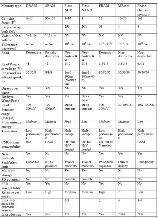
Table Captions
Chapter1
Table 1.1 Performance Comparison between volatile memory (DRAM and
SRAM) and nonvolatile memory (Flash, FRAM, MRAM and phase
change memory) devices. Among the nonvolatile memories, Flash
memory is the only memory compatible with the current CMOS
process flow. Overall, the Flash memory exhibits the best
performance except for the disadvantages of high programming
voltage and slow program/erase speed. ---10
Chapter2
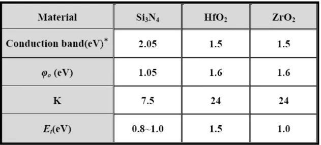
Table 2.1 Trapping material properties. ---25
Chapter3
Figure Captions
Chapter1
Fig1-1 Schematic cross section of the conventional floating gate nonvolatile
memory device. Poly-Si floating gate is used as the charge storage
element. ---11
Fig1-2 Schematic cross section of ETOX device. ---11
Fig1-3 I-V curves of a floating gate device. ---12
Fig1-4 Schematic cross section of the SONOS nonvolatile memory device. 12
Fig1-5 Energy band diagrams of SONOS Flash memory.---13
Chapter2
Fig2-1 The procedure of channel hot electrons injection (CHEI). ---26
Fig2-2 The approach of FN programming method. ---26
Fig2-3 The approach of MFN programming method. ---27
Fig2-4 The approach of TAT programming method. ---27
Fig2-5 Band diagram of a MOS structure along the vertical direction through the
depletion region illustrating band-to-band and trap-to-band tunneling
mechanisms. ---28
Fig2-6 The procedure of band to band hot electron injection. ---28
Fig2-7 The procedure of band to band hot hole injection. ---29
Fig2-8 Bandgap diagram of a SONOS device in the excess electron state,
showing retention loss mechanisms: trap-to band tunneling (T-B),
trap-to-trap tunneling (T-T), band-to-trap tunneling (B-T), thermal
excitation (TE) and Pool-Frenkel emission (PF). ---29
Fig2-9 Ideal energy band diagrams for SONOS and SOHOS structures. ---30
Fig2-10 Energy band diagram schematic of the SONOS structure with HfO
2(solid lines) or Si
3N
4(dashed lines) as the charge storage layer during
write (program) operations. ---30
Chapter3
Figure 3-1:(a)Schematic cross section oh the HfO2 SOHOS device. ---38
(b)Process flows for fabricating HfO2 SOHOS device. ---38
Figure 3-2:(a) The Ids-Vds Curves of HfO2 SOHOS device ---39
(b) The Ids-Vgs Curves of HfO2 SOHOS device ---39
Figure 3-3:(a)Program characteristics of N1 with different operating condition ---40
(b)Program characteristics of N2 with different operating condition ---40
Figure 3-4:(a)Program characteristics of N3 with different operating condition ---41
(b)Program characteristics of O1 with different operating condition ---41
Figure 3-5:(a)Program characteristics of O2 with different operating condition ---42
(b)Program characteristics of O3 with different operating condition ---42
Figure 3-6:(a)Program speed of tunnel layer as oxynitride with VD=VG=8V ---43
(b) Program speed of tunnel layer as oxide with VD=VG=8V ---43
Figure 3-7:(a)Program speed of N1 and O1with VD=VG=8V ---44
(b)Erase characteristics of N1 with different operating condition ---44
Figure 3-8:(a)Erase characteristics of N2 with different operating condition ---45
(b)Erase characteristics of N3 with different operating condition ---45
Figure 3-9:(a)Erase characteristics of O1 with different operating condition ---46
(b)Erase characteristics of O2 with different operating condition ---46
Figure 3-10:(a)Erase characteristics of O3 with different operating condition ---47
(b)Erase speed of tunnel layer as oxynitride with VG=-7 VD=7 ---47
Figure 3-11:(a)Erase speed of tunnel layer as oxynitride with VG=-7 VD=7 ---48
(b) The retention characteristics of N2 at room temperature ---49
Figure 3-13:(a) The retention characteristics of N3 at room temperature ---50
(b) The retention characteristics of O1 at room temperature ---50
Figure 3-14:(a) The retention characteristics of O2 at room temperature ---51
(b) The retention characteristics of O3 at room temperature ---51
Figure 3-15:(a) The endurance characteristics of N1 ---52
(b) The endurance characteristics of N2 ---52
Figure 3-16:(a) The endurance characteristics of N3 ---53
(b) The endurance characteristics of O1 ---53
Figure 3-17:(a) The endurance characteristics of O2 ---54
(b) The endurance characteristics of O3 ---54
Figure 3-18:(a) The retention characteristics of N1 after 104 cycles ---55
(b) The retention characteristics of O1 after 104 cycles ---55
Figure 3-19:(a) The retention characteristics of N1 at 125℃ ---56
CHAPTER 1
Introduction
1.1General Background
The application of semiconductor memory is more and more indispensable for the modern living. For instance, the semiconductor memories are used in personal computers, cellular phones, digital cameras, smart-media, networks, automotive systems, global positioning systems. Table 1.1 lists the characteristics of different types of semiconductor memory that either have been commercialized or are being developed in the industry.
Since the demonstration of the MOSFET in 1960, one of the most revolutionary technology driver to decide the direction of semiconductor industries development is the semiconductor memories. Because of the high cost, large volume, and high power consumption of the magnetic-core memory, the electronic industries urgently needed a new kind of memory device to replace the magnetic-core memory. In 1967, D. Kahng and S. M. Sze invented the first floating-gate (FG) nonvolatile semiconductor memory at Bell Labs [1]. To date, the stacked-gate floating gate device structure, as shown in Fig. 1-1, continues to be the most prevailing nonvolatile-memory implementation, and is widely used in both standalone and embedded memories. The invention of FG memory impacts more than the replacement of magnetic-core memory, and creates a huge industry of portable electronic systems. The most widespread memory array organization is the so-called Flash memory, which has a byte-selectable write operation combined with a sector “flash” erase.
attracted more and more attention due to the booming market of portable electronic devices such as cellular phones and digital cameras. These applications require the memory to have ten years data retention time, so that the nonvolatile memory (NVM) device has become indispensable. There are mainly four types of nonvolatile memory technology: Flash memory, Ferro-electric Random Access Memory (FeRAM), Magnetic Random Access Memory (MRAM) and Phase Change Memory (PCM).
Among four types of nonvolatile memory , Flash memory is presently the most suitable choice for the following reasons:
(1)FeRAM is not a perfect nonvolatile memory since its reading mode is a kind of destructive operation. A programming verification is required to restore the data after reading. On the contrary, Flash memory doesn’t need the additional action. This means that the reading operation of Flash memory is not destructive, and the operation affects slighter data retention disturbance than FeRAM.
(2) Flash memory can achieve the highest chip density. A Flash memory cell consists of only one transistor [2]. A FeRAM memory cell generally consists of one transistor and one capacitor [3], while a MRAM cell needs a transistor and a magnetic tunnel junction [4]. Phase Change Memory was expected to be a promising nonvolatile memory [5]; however, its memory cell consists of one resistor and a bipolar junction transistor. Until now, only a 256MB phase change memory chip has been demonstrated. It will take more effort to demonstrate whether the Phase Change Memory is really a promising technology.
(3) Flash memory possesses the multi-bit per cell storage property [6]. Four distinct threshold voltage (Vth) states can be achieved in a Flash memory cell by controlling the
amount of charge stored in its floating gate. Two-bits/cell (with four Vth states) Flash memory cells have already been commercialized. A four-bits/cell Flash memory device is feasible and is under development now [7]. Multi-bit storage increases memory density and thus reduces the cost per bit significantly. Furthermore, Matrix Semiconductor Inc. demonstrated multi-layer (sometimes called “three-dimensional integration”) SONOS Flash memory recently [8]. This novel idea offers another possibility to achieve even higher density and lower cost technologies based on Flash memory.
(4) Flash memory fabrication process is compatible with the current CMOS process and is a suitable solution for embedded memory applications. A Flash memory cell is simply a MOSFET cell, except that a poly-silicon floating gate [9] (or Silicon Nitride charge trap layer [8]) is sandwiched between a tunnel oxide and an inter-poly oxide to form a charge storage layer. All other nonvolatile memories require integration of new materials that are not as compatible with a conventional CMOS process. It is easier and more reliable to integrate Flash memory than other nonvolatile memories with logic and analog devices in order to achieve better chip performance for wireless communication and wireless computation [10].
Since Flash memory possesses above four key advantages, it has become the mainstream nonvolatile memory device nowadays.
The Flash memory cell structure was presented for the first time by D. Kahng and S. M. Sze in 1967. And the famous commercial Flash memory is Intel ETOX (EPROM Tunnel Oxide) structure in 1988 [11]. The ETOX device structure is shown in Fig. 1-2. The operation principal is using the underside poly-silicon which is named Floating Gate ( FG ) as the charge store unit for the device. And the ETOX are “written” and “erase” by
Channel-Hot-Electron (CHE) programming and Fowler-Nordheim tunneling (F-N) or Band-to-Band-Hot-Hole (BTBHH),respectively. After electrons which injected from channel, the threshold voltage of devices will be shifted. The logical “0”and “1” definition of nonvolatile memory devices are used for the difference between threshold voltage (Fig. 1-3). This detail of the concept will be described in Chapter 2.
Although a huge commercial success, conventional FG devices have their limitations. Two of the most primary limitations are: (1) the limited potential for continued scaling down of the device structure. This scaling down limitation results from the extreme requirements of the tunnel oxide layer. The tunnel oxide must be thin enough to allow quick and efficient charge transport to and from the floating gate (FG). On the other hand, the tunnel oxide needs to provide superior isolation under retention, endurance, and disturbed conditions in order to maintain information integrity over periods of up to a decade. When the tunnel oxide is thinner for operation speed consideration, the retention characteristics may be degraded. And when the tunnel oxide is made thicker to take the isolation into account, the speed of the operation will be slower. Therefore, for mass production, there is a trade-off between speed and reliability for the optimal tunnel oxide thickness. (2) The quality and strength of tunnel oxide after plenty of program/erase cycles. Once a leaky path has been created in the tunnel oxide, all the charges stored in the floating gate will be lost. Therefore, two suggestions, Poly-Silicon/Oxide/Nitride/Oxide/Silicon (SONOS) [12-14] and nanocrystal nonvolatile memory devices [15-17], are proposed to overcome this oxide quality limit of the conventional FG structure. These technologies replace the floating gate structure with a great number of charge-storage nodes in the dielectric or in the nanocrystal. Unlike the
floating gate, stored charges in isolated nodes cannot easily redistribute among themselves and the local leaky path will not cause the fatal loss of information for the nanocrystal nonvolatile memory device. This effectively prevents the leakage of all the stored charges out of the floating gate.
The charge storage elements in SONOS memory (Fig. 1-4 ) are the charge traps distributed throughout the volume of the Si3N4 layer. A typical trap has a density of the order 1018~1019 cm-3 according to Yang et al [18] and stores both electrons and holes (positive charges) injected from the channel. The nitride-based memory devices were extensively studied in the early 70s after the first metal-gate nitride device metal/nitride/oxide/silicon (MNOS) was reported in 1967 by Wegener et al [19]. Initial device structures in the early 1970s were p-channel metal-nitride-oxide-silicon (MNOS) structures with aluminum gate electrodes and thick (45nm) silicon nitride charge storage layers. Write/erase voltages were typically 25-30 V. In the late 1970s and early 1980s, scaling moved to n-channel silicon-nitride-oxide-silicon (SNOS) devices with write/erase voltages of 14-18 V. In the late 1980s and early 1990s, n- and p-channel SONOS devices emerged with write/erase voltages of 5-12 V. In the SONOS device, an oxide layer is introduced between the gate and the nitride region. Thus, it forms the SiO2/Si3N4/SiO2 (ONO) gate dielectric stack instead of capping the nitride layer with just a metal or semiconductor gate. The purpose of the top blocking oxide is to reduce the charge injection from the control gate into the nitride layer, limiting the memory window of both MNOS and SNOS devices.
channel can tunnel across the SiO2 into the nitride layer. Some electrons will continue to move through the nitride layer then across the control oxide finally into the control gate. The remaining trapped charges in the nitride layer provide the electrostatic screening of the channel from the control gate. Therefore, there is a threshold voltage (Vth) shift resulting from trapped charges in nitride and because of that SONOS can be used as a memory device just like conventional floating gate devices.
In past decade, about 20% of semiconductor market is given by the semiconductor memory. And the output value of Flash memory is expected to reach US$ 60 billions in 2010. Developing the higher-capacity and faster Flash nonvolatile memory is always one of the most important issues for a wide range of applications. In order to pursue the goal, down sizing or multi-bit is the key point for pushing next generation development. And the most important performances of Flash memory are reliability characteristics, such as program/erase cycling and data retention. It is well known that the tunnel oxide
degradation during FN (Fowler-Nordheim) stress is due to the oxide trap and interface trap generation. Thus, how to improve the reliability of Flash memory is the focus in this study.
1.2 Motivation
According to the International Technology Roadmap for Semiconductors (ITRS) [20], high-k dielectric materials would be able to maintain an equivalent potential difference from the floating gate to the device body for a larger thickness compared to . The charge leakage of trap layer would be minimized and the scaling limits would be extended.
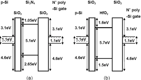
In addition, using high-k dielectric trapping layer (which is called SOHOS, Poly-Silicon/Silicon-Oxide/High-k/Silicon-Oxide/Silicon) show some advantages, for instance, high program/erase speed, easy to fabricate, low power consumption and low programming voltage, better potential for scalability below the 70-nm node, according the ITRS. Hafnium oxide (HfO2) is consider to replace the Si3N4 trapping layer of SONOS-type Flash memory[21]. HfO2 is expected to have better charge trapping characteristics than the conventional Si3N4 film. Because of the density of trap state and deep trap energy level SOHOS can achieve longer retention time than SONOS [22-24].
Although SONOS Flash memory device has attracted much attention due to its advantages over the traditional floating-gate Flash memory device, it still faces challenges for further improvement. For example, the tunnel oxide thickness cannot be reduced below 25Å to improve the programming speed, if 10-years retention time must be guaranteed [25]. As shown in Fig. 1-5, there are two charge-loss mechanisms:
(1) direct tunneling, with an associated barrier height φo+Et ; and (2) thermally assisted de-trapping into the nitride conduction band and subsequent tunneling through the tunnel oxide, with associated barrier height φo. A high conduction band offset φo between the trapping layer and the tunnel oxide is essential for achieving long retention time. The offset φo for a nitride trapping layer is only 1.05 eV and the offset φo for HfO2 trapping layer is up to 1.6 eV. Because of the valid reason we choose the HfO2 film as the trapping lever rather than Si3N4 film in this research.
The other method to modify the retention and endurance of Flash memory is improving the tunnel oxide quality and strength. When the Flash memory device through
plenty of program/erase (P/E) cycles, the tunnel oxide degradation during FN (Fowler-Nordheim) stress is due to the oxide traps and interface traps generation. If the oxide thickness is reduced below 10nm, high-field stress manifests through a degradation of the insulating properties of the oxide well before the occurrence of breakdown. Stress-induced leakage currents (SILC) are responsible for serious data retention problems in Flash memory and represent the main concern in the process of scaling the tunnel oxide thickness to lower values. Thus, a JVD silicon-nitride was studied to replace the dry tunnel oxide due to its higher dielectric constant and the low stress-induced leakage current (SILC) in recently years [26-27]. However, the interface between Nitride/Silicon is not as good as the SiO2/Silicon interface and the Si-SiN barrier height is lower than that of Si-SiO2 [27-28]. Therefore, the oxide layer with nitrogen treatment (called Oxynitride film) is also a popular choice and has been studied broadly because of its excellent endurance [29-30]. This film proves the promising candidate to substitute thermal oxide right now.
In this study, we propose a novel process for forming an ultrathin oxynitride film with high nitrogen topping. The oxynitride growth includes three main process stages- chemical oxide growth, nitridation and subsequent dry oxidation. By this technique, the desirable nitrogen concentration profile can be obtained to meet the requirement of device performance. By replacing the conventional dry oxide film with novel oxynitride film, we expect to advance the reliabilities of the Flash memories.
1.3 Organization of This Thesis
described as follows.
In chapter 1, the potential memory devices about nonvolatile memory (NVM) 、 conventional Flash、SONOS and SOHOS devices are introduced in this chapter.
In chapter 2, this section focuses on the basic program and erase mechanisms of Flash memory device.
In chapter 3, the SOHOS structure with HfO2 trapping layer, oxynitride and oxide as tunnel oxide layer is proposed in this section. Finally, compare the oxynitride layer with conventional oxide layer, the device characteristics will be discussed between two different tunnel oxide process conditions.
Table 1.1: Performance Comparison between volatile memory (DRAM and SRAM) and nonvolatile memory (Flash, FRAM, MRAM and phase change memory) devices. Among the nonvolatile memories, Flash memory is the only memory compatible with the current CMOS process flow. Overall, the Flash memory exhibits the best performance except for the disadvantages of high programming voltage and slow program/erase speed.
Fig1-1: Schematic cross section of the conventional floating gate nonvolatile memory device. Poly-Si floating gate is used as the charge storage element.
Fig1-3: I-V curves of a floating gate device when there is no charge stored in the FG (“1”-curve) and when a negative charge Q is stored in the FG (“0”-curve).
Fig1-4: Schematic cross section of the SONOS nonvolatile memory device. The nitride layer is used as the charge-trapping element.
Fig1-5: Energy band diagrams of SONOS Flash memory. Large 0
ϕ will block electron
CHAPTER 2
Basic Principles of Nonvolatile Memory
2.1 Program/Erase Operation Mechanisms
Most of operations on novel nonvolatile memories, such as nanocrystal and SONOS memories are base on the concept of Flash memory. If charge has to be stored in a bit of the memory, there are some different procedures. The threshold voltage shift of a Flash memory transistor can be written as [31-32]:
... .2 1
TH FCQ
V
e
C
Δ
= −
q
−
where Q is a negative charge stored in the FG, and CFC is the capacitances between the floating gate (FG) and control gate. The threshold voltage of the memory cell can be altered by changing the amount of charge present between the gate and the channel, corresponding to the two states of the memory cell, i.e., the binary values (“1” and “0”) of the stored bit. Figure 1-3 shows the threshold voltage shift between two states in a Flash memory. Regarding a nonvolatile memory, it can be “written” into either state “1” or “0” by either “programming” or “erasing” operation, which are decided by the
definition of memory cell itself. There are many solutions to achieve “programming” or “erasing”. In general, hot carrier electron injection (HCEI), F-N tunneling and band to band tunneling (BTBT), are three kinds of common operation mechanism employed in novel nonvolatile memories. The three mechanisms will lead difference characteristics for nonvolatile memories.
2.1.1 Channel Hot-Electron Injection (CHEI)
The physical mechanism of CHEI is relatively simple to understand qualitatively. An electron traveling from the source to the drain gains energy from the lateral electric field and loses energy to the lattice vibrations (acoustic and optical phonons). At low fields, this is a dynamic equilibrium condition, which holds until the field strength reaches approximately 100kV/cm [33]. For fields exceeding this value, electrons are no longer in equilibrium with the lattice, and their energy relative to the conduction band edge begins to increase. Electrons are “heated” by the high lateral electric field, and a small fraction of them have enough energy to surmount the barrier between oxide and silicon conduction band edges. Figure 2-1 shows schematic representation of CHEI MOSFET and the energy-distribution function with different fields. Electrons flowing from source to drain gain energy from the high-field region near the drain junction. The electrons arriving at the Si- SiO2 interface near the drain junction with enough energy to surmount the surface barrier are emitted into the SiO2 layer.The gate current is composed of those electrons which pass over the potential barrier between the channel and the gate. For an electron to cross this potential barrier three conditions must hold[34]:
(1) Its kinetic energy has to be higher than the potential barrier. (2) It must be directed toward the barrier.
(3) The field in the oxide should be collecting it.
This hot-electron emission is an attenuated version of the programming current developed in certain PROM devices
During programming, the positive voltages applied to the gate and drain while the source is grounded. These voltages generate a lateral and vertical electric field along the
channel. The electrons will move from the source to the drain and be accelerated by high lateral field near the drain junction in the channel. Once the electrons gain enough energy, they can surpass the energy barrier of the oxide layers and inject into trapping layer and be trapped. The current density of CHEI is expressed as
( ) 2 /
... .2 2
b Em m inj d ds bE
I
A I
λ
e
ϕ λeq
ϕ
−⎛
⎞
=
⎜
⎟
−
⎝
⎠
Here Ids is the channel current and Adis a constant.
2.1.2 Tunneling Injection
Tunneling mechanisms are demonstrated in quantum mechanics. Basically, tunneling injection must to have available states on the other side of the barrier for the carriers to tunnel into. If we assume elastic tunneling, this is a reasonable assumption due to the thin oxide thickness involved. Namely, no energy loss during tunneling processes. The tunneling probability, depending on electron barrier height (ϕ(x) ), tunnel dielectric
thickness ( d ), and effective mass ( me ), is express as
* 0
( )
exp
2
... .2 3
d ex m
T
=
⎛
⎜
−
ϕ
dx
⎞
⎟
−
⎜
⎟
⎝
∫
h
⎠
eq
Tunneling through the oxide can be attributed to different carrier-injection mechanisms. Which process applies depends on the oxide thickness and the applied gate field or voltage. Direct tunneling (DT), Fowler-Nordheim tunneling (FN), modified Fowler-Nordheim tunneling (MFN) and trap assistant tunneling (TAT) are the main programming mechanisms employed in memory [35-38].
2.1.2-(a) Direct Tunneling (DT)
For nanocrystal memories, the control-gate coupling ratio of nanocrystal memory devices is inherently small [39]. As a result, FN tunneling cannot serve as an efficient write/erase mechanism when a relatively thick tunnel oxide is used, because the strong electric field cannot be confined in one oxide layer. The direct tunneling is employed in nanocrystal memories instead. In the other hand, the direct tunneling is more sensitive to the barrier width than barrier height, two to four orders of magnitude reduction in leakage current can still be achieved if large work function metals, such as Au or Pt [40].
2.1.2-(b) Fowler–Nordheim Tunneling (FN)
The Fowler–Nordheim (FN) tunneling mechanism occurs when applying a strong electric field (in the range of 8~10MV/cm) across a thin oxide. In these conditions, the energy band diagram of the oxide region is very steep. Therefore, there is a high probability of electrons’ passing through the energy barrier itself. Using a free-electron gas model for the metal and the WKB (Wentzel-Kramers-Brillouim) approximation for the tunneling probability [41], one obtains the following expression for current density [42]:
(
*)
1/ 2(
)
3/ 2 2exp
8
2
... .2 4
3
ox B ox oxm
q
J
E
eq
hqE
π
⎡
−
Φ
⎤
⎢
⎥
=
−
⎢
⎥
⎣
⎦
Where Φ B is the barrier height (3.1eV for Si-SiO2) , m*oxis the effective mass of the
electron in the forbidden gap of the dielectric, h is the Planck’s constant, q is the
electronic charge, and Eox is the electric field which is defined as the applied voltage
tunneling mechanism.
2.1.2-(c) Modified Fowler–Nordheim Tunneling (MFN)
Modified Fowler–Nordheim tunneling (MFN) is similar to the traditional FN tunneling mechanism, yet the carriers enter the nitride at a distance further from the tunnel oxide-nitride interface. MFN mechanism is frequently observed in SONOS memories. The SONOS memory is designed for low-voltage operation (<10V, depending on the Equivalent oxide thickness), a relatively weak electrical field couldn’t inject charges by DT or FN tunneling mechanism. Figure 2-3 shows the MFN tunneling mechanism.
2.1.2-(d) Trap Assistant Tunneling (TAT)
The charge storage mediums with many traps may cause another tunneling mechanism. For example, the charges tunnel through a thin oxide and arrive to the traps of nitride layer at very low electrical field in SONOS systems. During trap assisted injection the traps are emptied with a smaller time constant then they are filled. The charge carriers are thus injected at the same distance into the nitride as for MFN injection. Because of the sufficient injection current, trap assistant tunneling may influence in retention [43]. Figure 2-4 shows the TAT tunneling mechanism.
3 * 3 * 2 3 2 1/ 2
2
4 2
exp
... .2 5
4
3
qpp g b b gm q V
m E
J
e
E
q
ε
π
ε
−⎡
⎤
⎢
⎥
=
−
⎢
⎥
⎣
⎦
h
h
q
−
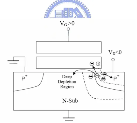
In MOS structures, band-to-band tunneling typically occurs at high source or drain voltage and low gate voltage. In Flash memory devices, these conditions take place in cells under erase operations, or in unselected cells sharing the same bit line with a cell under programming. BTBT contributes to the so called Gate Induced Drain Leakage current (GIDL) [44-45] , which can be a significant fraction of the subthreshold drain leakage current and can compromise proper functioning of the substrate bias generators.
Band to band tunneling application to nonvolatile memory was first proposed in1989. I. C. Chen and et al. demonstrated a high injection efficiency (~1%) method to programming EPROM devices [46]. Band-to-band Tunneling (BTBT) process occurs in the deeply depleted doped surface region under the gate to drain or gate to source overlap region. Figure 2-5 shows the band diagram of a MOS and illustrates BTBT mechanism. In this condition, the band-to-band tunneling current density is expressed as
2.1.3-(a) Band to Band Hot Electron Tunneling Injection
When band-bending is higher than the energy gap of the semiconductor, the tunneling electron from the valence band to the conduction band becomes significant. The mechanism is at the condition for positive gate voltage and negative drain voltage. Hence, the hot electrons are injected through the tunnel oxide and then recombine the stored holes as shown in Figure 2-6.
2.1.3-(b) Band to Band Hot Hole Tunneling Injection
The injection is applied for p-type substrate nonvolatile memory device. The mechanism is at the condition for negative gate voltage and positive drain voltage. Hence, the hot holes are injected through the tunnel oxide and then recombine the stored
electrons as shown in Figure 2-7.
2.2 Nonvolatile Memory Device Reliability
For a nonvolatile memory, the performance worthy to concern is distinguishing between two states of memory cell. However, in many times operation and charges storage for a long term, the states are not easily distinguishable because of charges loss. The nonvolatility of NVM implies at least 10 years of charge retention, and the cell has to store information also after many read/program/erase cycles. Endurance (also called Cycling) and retention experiments are performed to investigate Flash memory cell reliability.
2.2.1 Retention
As in any nonvolatile memory technology, Flash memories are specified to retain data for over ten years. This means the loss of charge stored in the FG must be as
minimal as possible. In updated Flash technology, due to the small cell size, the capacitance is very small and at an operative programmed threshold shift—about 2V- corresponds a number of electrons in the order of 103 to 104. A loss of 20% in this number (around 2–20 electrons lost per month) can lead to a wrong read of the cell and then to a data loss.
For SONOS memory devices, data are represented as electrons stored in the silicon nitride layer, the stored electrons leak away from the trapping layer through the tunnel oxide or through the interpoly dielectrics; moreover, the lateral migration of charges trapped in the silicon nitride layer also result in the wrong information [47-48].
Possible causes of charge loss are: (1) by tunneling or thermionic emission mechanisms; (2) defects in the tunnel oxide; and (3) detrapping of charge from insulating layers surrounding the storage medium.
First, several discharge mechanisms may be responsible for time and temperature dependent retention behavior of nonvolatile memory devices. Figure 2-8 shows a bandgap diagram of a SONOS device in the excess electron state, illustrating trap-to-band tunneling, trap-to-trap tunneling, and band-to-trap tunneling, thermal excitation and Poole-Frenkel emission retention loss mechanisms [49]. These mechanisms may be classified into two categories. The first category contains tunneling processes which are not temperature sensitive (trap-to-band tunneling, trap-to-trap tunneling and band-to-trap tunneling). The second category contains the other mechanisms which are temperature dependent. Moreover, trapped electrons may redistribute vertically inside the nitride by Poole–Frenkel emission, which will give rise to a shift in the threshold voltage.
Secondly, the generation of defects in the tunnel oxide can be divided into an extrinsic and an intrinsic one. The former is due to defects in the device structure; the latter to the physical mechanisms which are used to program and erase the cell. Finally, electrons can be trapped in the insulating layers surrounding the storage medium during wafer processing. The electrons can subsequently de-trap with time, especially at high temperature. However, the charge variation results in a variation of the storage medium potential.
which usually adopt high electric fields and hostile environments at high temperature.
2.2.2 Endurance
Endurance is the number of erase/write operations that the memory can still
complete and continue to operate as specified in the data sheet. In general, Flash cells are requested to guarantee 105 erase/program cycles. This endurance requirement is sufficient for the user to take 700 photos with a 1MB size every day for 10 years [48].Endurance of Flash memory can be limited by two failure modes: 1) the reduction of p/e efficiency due to oxide aging, which brings to a parametric failure, 2) single-cell failures due to tunnel oxide defects.
As the experiment was performed applying constant pulses, the variations of program and erase threshold voltage levels are described as “program/erase threshold voltage window closure” and give a measure of the tunnel oxide aging [50-51]. In particular, the reduction of the programmed threshold with cycling is due to trap generation in the oxide and interface state generation at the drain side of the channel. The evolution of the erase threshold voltage reflects the dynamics of net fixed charge in the tunnel oxide as a function of the injected charge. The initial lowering of the erase is due to a pile-up of positive charge which enhances tunneling efficiency, while the long-term increase of the erase is due to a generation of negative traps.
The endurance characteristics give the memory threshold voltage window, which is the threshold voltages difference between the programmed state and the erased state. It is the parameters to describe how reliable is a nonvolatile memory cell. The program/erase
cycles are usually measured by the FN tunneling or channel hot electron injection mechanism under room temperature environment.
2.3 High-k Material as Trapping Layer
In order to improve the programming speed and/or lower the programming voltage of a SONOS-type memory device, it is desirable to use a trapping material with a lower conduction band edge (higher electron affinity) to achieve a larger offset φo, as well as to
provide for programming by direct tunneling at low voltages. Recently, high-k (“high-permittivity”) dielectric materials such as HfO2 and ZrO2 have been investigated to replace thermal oxide as the MOSFET gate dielectric [52-53]. A comparison of dielectric material properties is given in Table 2.1. Such materials have a lower conduction band edge than does silicon nitride. Thus, it should be advantageous to use a high-k material as the trapping layer in a SONOS-type memory device, provided that it contains a sufficient density of deep trap states. The electron trap level Et has been
reported to be 1.0 eV for ZrO2 [52]; it has been reported to be 1.5eV for JVD HfO2 [53]. In principle, the trap density and trap energy level in a high-k trapping layer can be tuned by adjusting the deposition process parameters.
For SOHOS (Poly-Silicon/Oxide/High-k/Oxide/Silicon) devices, the charges may be trapped in electron and hole traps in the HfO2 layer or by charge confinement in the quantum well. From the ideal energy band diagrams of SONOS and SOHOS structures shown in Fig. 2-9 (a) and (b), respectively, the quantum well formed by the conduction band is deeper for the SOHOS structure as compared to the SONOS structure (1.6 eV
Fowler–Nordheim (MFN) tunneling dominates, the electrons must tunnel through a thicker energy barrier in SONOS to the conduction band of the charge storage layer (Si3N4) as compared to SOHOS. The conduction band offset of Si3N4 with respect to silicon is 2.05 eV, as compared to a 1.5 eV conduction band offset of HfO2 with respect to silicon. This is illustrated in Fig. 2-10, where the modified F–N tunneling consists of direct tunneling through the thin tunnel oxide layer and F–N tunneling through the charge storage layer. Hence, electron tunneling and storage in the quantum well will be easier in SOHOS as compared to SONOS devices.
Fig 2-1: The procedure of channel hot electrons injection (CHEI).
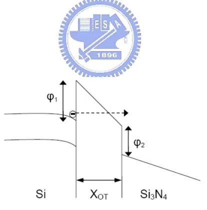
Fig 2-2: The approach of FN programming method, when
1OT OT E X φ >
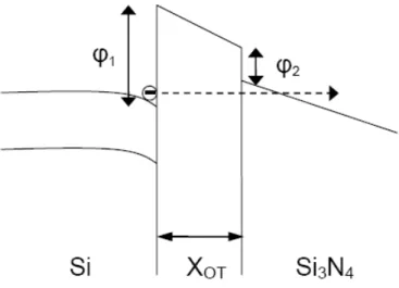
Fig 2-3: The approach of MFN programming method,
when
1 2 1 2 OT OX OT OT N N E X X X φ φ φ φ ε ε − > > − ⎛ ⎞ + ⎜ ⎟ ⎝ ⎠Fig 2-4: The approach of TAT programming method,
when
3 3 3 1 2 , OT t OX OT OT N N E X X X φ φ φ φ φ φ ε ε > > = − − ⎛ ⎞ + ⎜⎝ ⎟⎠Fig 2-5: Band diagram of a MOS structure along the vertical direction
through the depletion region illustrating band-to-band and
trap-to-band tunneling mechanisms.
V
G>0
Fig 2-7: The procedure of band to band hot hole injection.
Fig 2-8: Bandgap diagram of a SONOS device in the excess electron state,
showing retention loss mechanisms: trap-to band tunneling (T-B),
trap-to-trap tunneling (T-T), band-to-trap tunneling (B-T),
Fig 2-9: Ideal energy band diagrams for (a) SONOS and (b) SOHOS
structures.
Si
3N
4Fig2-10: Energy band diagram schematic of the SONOS structure with
HfO
2(solid lines) or Si
3N
4(dashed lines) as the charge storage
layer during write (program) operations.
CHAPTER 3
Device Fabrication and Characterization
3.1 Introduction
Polysilicon–oxide–nitride–oxide–silicon (SONOS) Flash memory is one of the most attractive candidates to realize Flash vertical scaling. An increase in the
programming speed of SONOS devices and a lower voltage operation has been
previously accomplished by reducing the tunnel-oxide thickness. However, this seriously degrades the charge-retention capability of the device. To overcome this limitation, the so-called polysilicon–oxide–high-κ–oxide–silicon (SOHOS) Flash memory has been attempted by replacing the silicon nitiride layer with a high-dielectric constant (high-κ) material. The SOHOS structure, with hafnium oxide (HfO2) as the charge-storage layer, demonstrates a superior charge-storage capability at low voltages, faster programming, and less over-erase problems compared to conventional SONOS devices.
Poly-Silicon/Oxide/High-k/Oxide/Silicon (SOHOS) structure, stores charges in spatial deep level traps, making it less vulnerable to a single defect in the tunnel oxide. This significantly helps to minimize the discharge of the memory cell [56]. During the program operation of the SOHOS n-channel transistor device, electrons tunneled through the tunnel oxide and are stored in the deep level traps [57]. During the erase operation under negative gate bias, electrons trapped in the high-k material are detrapped via tunneling through the oxide layer into the silicon substrate. Therefore, the HfO2 material is selected in our research and we will look for the optimum process conditions.
trapping amount and the low stress-induced leakage current [58-59]. In general, benefit of a silicon oxynitride film is that the nitrogen accumulates at the silicon interface to reduce the concentration of strained Si-O bond and the creation of hot electrons as many as three orders of magnitude. Nowadays, lower process temperature and thinner oxynitride films are preferred in ULSI technology. In this study, we proposed a novel approach for forming an oxynitride tunnel dielectric with high nitrogen content. In the oxyenitride, we can obtain Si-rich at the bottom and N-rich at the top. The desirable structure can be obtained to meet the requirement of the SONOS type nonvolatile memory device performance.
3.2 Experiments
3.2.1 Fabrication of HfO
2Trapping Layer Memory Device
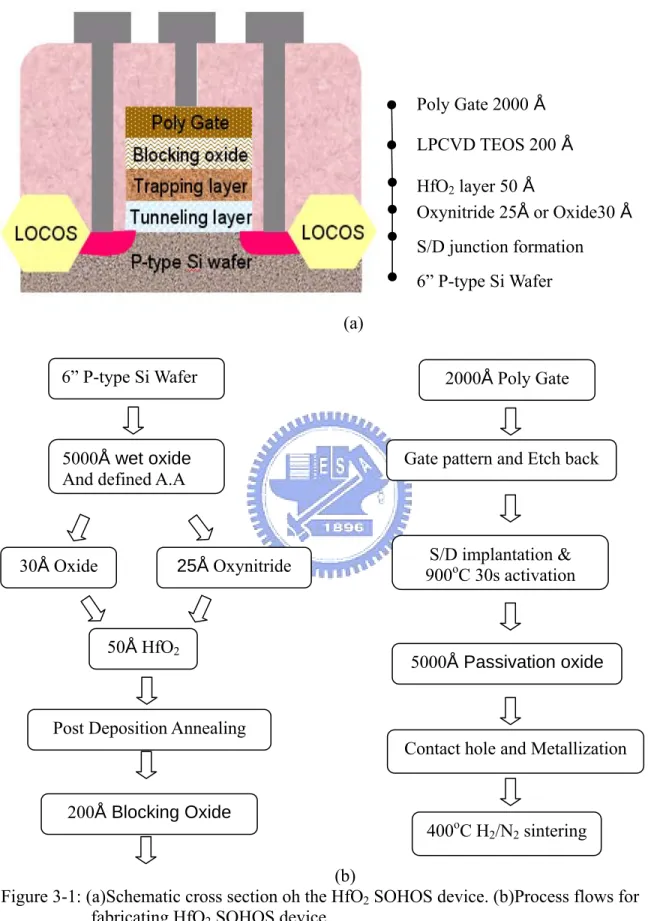
Figure 3-1 (a)-(b) schematically depicts the cross-section and the process flow of the SOHOS Flash memory cell with HfO2 trapping layer. The experimental process of the memory device were carried out on 6-inch p-type (100)-oriented silicon substrate wafers. First of all, the wafers were cleaned down by standard RCA cleaning. Before growing the tunnel oxide film, the all wafers were dipped into diluted HF solution to remove the chemical oxide which grown during the standard RCA cleaning.
In the same way, the characteristics of HfO2 memory devices should be compared between the control and experimental samples. Therefore, the tunnel oxide of control sample grew in atmospheric furnace at 900 . Subsequently, the experimental devices ℃ were steeped into H2O2 solution at room temperature immediately. The immersion
process let wafers grow about 10 Å chemical oxide in 20 min. Then the chemical oxide carried out the nitridation process through LPCVD (Low Pressure Chemical Vapor Deposition) furnace in low-pressure (180 mTorr) NH3 ambient at 750℃ for 15 min. Next, the nitrided chemical oxide was placed in atmospheric O2 ambient at 900 for 70 sec. ℃ Now, the whole tunnel oxide process is completed, and the initial chemical oxide already become the oxynitride film. Then 45~50 Å HfO2 film was deposited by MOCVD ( Metal organic chemical vapor deposition ), followed by post-deposition annealing (PDA) in the nitrogen ambient using a RTA (Rapid Temperature Annealing) system. Afterward, about 200 Å blocking oxide was deposited by LPCVD TEOS. Then, the poly-silicon gate 2000 Å is formed by LPCVD at 900 for 30 min. After poly℃ -silicon/blocking oxide/HfO2/tunnel oxide stack formation, gate pattern were defined by lithography and etched back. Subsequently, The transistors undergo source/drain implantation, followed by activation annealing at 950℃ for 30 s. Next, the passivation layer 5000 Å by LPCVD followed removing on the gate, source and drain region. Then we define the contact hole by lithography and BOE etching back.
Lastly, the top electrode about 9000 Å aluminum (Al-Si-Cu) metal film was deposited by sputtering system. Then the Al film was patterned and sintered to define the metal pad. Figure 3-4 schematically describes the construction of measurement system. The electrical characteristics of SOHOS memory device and test capacitors are measured by HP4284 Precision LCR Meter and HP4156C Precision Semiconductor Parameter Analyzer. The transistor structures tested have gate width to gate length dimensions of W/L = 1/10 mμ .
3.3 Results and Discussions
3.3.1 Electrical Characteristic of HfO
2Memory Device
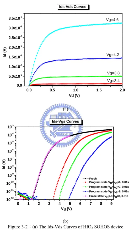
This section will analyze the electric characteristics of the SOHOS Flash memory with HfO2 trapping layer. in N2 ambient and the split table is listed in Table 3.1. Fig 3.2(a) shows the ID-VD curve and Fig 3.2(b) show s the ID-VG curve of Flash memory devices. When the device programmed, the electron was trapped in the HfO2 layer and make the Vth shift to positive side. When the device erased, the electron was detrapped and make the Vth. return the initial state. The memory devices are programmed by CHE., as shown in Fig 3-3 (a), Fig 3-3 (b), Fig 3-4(a), Fig 3-4(b), Fig 3-5(a), Fig 3-5(b). The CHE (channel hot electron) program is to set VD=VG=6V、VD=VG=7V、VD=VG=8V and VD=VG=9V.We compare the program speed of tunnel layer as oxynitride with different PDA in Fig 3-6(a), and as oxide with different PDA in Fig 3-6(b). We can observe that the program speed of device undergo higher PDA slightly higher than the others. The reason for faster program speed is that HfO2 trapping layer is more crystallized and induce more traps .The compared program speed of tunnel layer as oxynitride or oxide in Fig 3-7 (a). We can observe that the tunnel layer as oxynitride faster than oxide. It is attributed to the thinner tunnel oxide of N1. Because the more electric field across the thinner tunnel oxide.
The memory devices are erased by The BTBT tunneling, as shown in Fig 3-7 (b) , Fig 3-8 (a), Fig 3-8(b) , Fig 3-9 (a) , Fig 3-9 (b) , Fig 3-10 (a).The BTBT erase is to set VG=-5V VD=5 V、VG=-6V VD=6 V、VG=-7V VD=7 V、VG=-8V VD=8 V. We compare the erase speed of tunnel layer as oxynitride with different PDA in Fig 3-10(b) ,and as oxide with different PDA in Fig 3-11(a). The compared erase speed of
tunnel layer as oxynitride or oxide in Fig 3-11 (b). The tunnel layer as oxynitride faster than oxide. The reason as like as program.
Subsequently, the compared retention property of tunnel layer as oxynitride or oxide is shown in Fig 3-12(a), Fig 3-12(b), Fig 3-13(a), Fig 3-13(b), Fig 3-14(a), Fig 3-14(b). The result that the devices undergo lower PDA performs the better retention characteristic is observable. The data retention degradation attributes to the charge loss. Some possible causes of charge loss are defects in tunnel oxide, defects in blocking oxide or mobile ion contamination. Therefore, we thought that higher PDA will induce more traps with shallower energy level in the trapping layer, which give rise to larger window and poor charge retention[64].
The compared endurance property of tunnel layer as oxynitride or oxide is shown in in Fig 3-15(a), Fig 3-15(b), Fig 3-16(a), Fig 3-16(b), Fig 3-17(a), Fig 3-17(b).
The tunnel layer as oxynitride owned slightly better retention. In order to further confirm the improvement, the retention after 104 program/erase cycles in Fig 3-18(a), Fig 3-18(b) and the retention at 125℃ in Fig 3-19(a), Fig 3-19(b). These retention results reveal that the oxynitride process can reduce the defects of tunnel oxide and reform the data integrity of Flash memory.
3.4 Summary
From experimental data and analysis, oxynitride as tunneling layer perform better
rentention after 104 program/erase cycles and at 125℃ than dry oxide. When tunnel oxide scale down to 3nm, the oxynitride can replace thermal oxide as the SOHOS tunnel layer. If we replace conventional oxide with oxynitride process technology, the interface state and defects generation
after repeatedly operation can be diminished. In this study, a novel memory structure, based on the oxynitride as tunneling layer, the HfO2 as trapping layer, is to achieve faster programming and better retention performance.
PDA700℃ 30sec
PDA700℃ 60sec
PDA800℃ 30sec
Oxynitride
Layer(25
Αo)
N1 N2 N3
Oxide layer
(30
Αo)
O1 O2 O3
(a)
(b)
Figure 3-1: (a)Schematic cross section oh the HfO2 SOHOS device. (b)Process flows for fabricating HfO2 SOHOS device.
2000Å Poly Gate
Gate pattern and Etch back
S/D implantation & 900oC 30s activation 5000Å Passivation oxide LPCVD TEOS 200 Å HfO2 layer 50 Å Poly Gate 2000 Å Oxynitride 25Å or Oxide30 Å S/D junction formation 6” P-type Si Wafer 6” P-type Si Wafer 5000Å wet oxide And defined A.A
30Å Oxide 25Å Oxynitride
50Å HfO2
Post Deposition Annealing
Contact hole and Metallization
200Å Blocking Oxide
400oC H
0.0 0.5 1.0 1.5 2.0 0.0 5.0x10⁻⁶ 1.0x10⁻⁵ 1.5x10⁻⁵ 2.0x10⁻⁵ 2.5x10⁻⁵ 3.0x10⁻⁵ 3.5x10⁻⁵ Ids-Vds Curves Id ( A ) Vd (V) Vg=4.6 Vg=4.2 Vg=3.8 Vg=3.4 (a) 0 1 2 3 4 5 6 7 8 9 10-12 10-11 10-10 10-9 10-8 10-7 10-6 10-5 10-4 10-3 Ids-Vgs Curves Id (A) Vg (V) Fresh Program state VD=VG=6, 0.01s Program state VD=VG=7, 0.01s Program state VD=VG=8, 0.01s Erase state VG=-8 VD=8, 0.01s (b)
Figure 3-2:(a) The Ids-Vds Curves of HfO2 SOHOS device (b) The Ids-Vgs Curves of HfO2 SOHOS device
10-6 10-5 10-4 10-3 10-2 10-1 100 0 1 2 3 4 5 6 7 Pulse Width (s) VD=VG=6 VD=VG=7 VD=VG=8 VD=VG=9 Oxynitride RTA700oC 30s Δ V th (V ) (a) 10-6 10-5 10-4 10-3 10-2 10-1 100 0 1 2 3 4 5 6 7 Pulse Width (s) Oxynitride RTA700oC 60s Δ V th (V ) VD=VG=6 VD=VG=7 VD=VG=8 VD=VG=9 (b)
Figure 3-3:(a)Program characteristics of N1 with different operating condition (b)Program characteristics of N2 with different operating condition
10-6 10-5 10-4 10-3 10-2 10-1 100 0 1 2 3 4 5 6 7 Pulse Width (s) Oxynitride RTA800oC 30s VD=VG=6 VD=VG=7 VD=VG=8 VD=VG=9 Δ Vth (V) (a) 10-6 10-5 10-4 10-3 10-2 10-1 100 0 1 2 3 4 5 6 7 Pulse Width (s) Oxide RTA700oC 30s Δ V th (V) VD=VG=6 VD=VG=7 VD=VG=8 VD=VG=9 (b)
Figure 3-4:(a)Program characteristics of N3 with different operating condition (b)Program characteristics of O1 with different operating condition
10-6 10-5 10-4 10-3 10-2 10-1 100 0 1 2 3 4 5 6 7 Pulse Width (s) Oxide RTA700oC 60s VD=VG=6 VD=VG=7 VD=VG=8 VD=VG=9 Δ Vth (V) (a) 10-6 10-5 10-4 10-3 10-2 10-1 100 0 1 2 3 4 5 6 7 Pulse Width (s) Oxide RTA800oC 30s VD=VG=6 VD=VG=7 VD=VG=8 VD=VG=9 Δ V th (V) (b)
Figure 3-5:(a)Program characteristics of O2 with different operating condition (b)Program characteristics of O3 with different operating condition
10-6 10-5 10-4 10-3 10-2 10-1 100 0 1 2 3 4 5 6 7 VD=VG=8 Pulse Width (s) Δ Vth (V ) Program speed Oxynitride RTA700oC 30s Oxynitride RTA700oC 60s Oxynitride RTA800oC 30s (a) 10-6 10-5 10-4 10-3 10-2 10-1 100 0 1 2 3 4 5 6 VD=VG=8 Δ V th (V ) Program speed Pulse Width (s) Oxide RTA700oC 30s Oxide RTA700oC 60s Oxide RTA800oC 30s (b)
Figure 3-6:(a)Program speed of tunnel layer as oxynitride with VD=VG=8V (b) Program speed of tunnel layer as oxide with VD=VG=8V
10-6 10-5 10-4 10-3 10-2 10-1 100 0 1 2 3 4 5 6 7 Program speed Δ V th (V ) Pulse Width (s) Oxynitride RTA700oC 30s Oxide RTA700oC 30s VD=VG=8 (a) 10-7 10-6 10-5 10-4 10-3 10-2 10-1 100 0 1 2 3 4 5 6 Pulse Width (s) Oxynitride RTA700oC 30s Δ Vth (V) VG=-5,VD=5 VG=-6,VD=6 VG=-7,VD=7 VG=-8,VD=8 (b)
Figure 3-7:(a)Program speed of N1 and O1with VD=VG=8V
10-7 10-6 10-5 10-4 10-3 10-2 10-1 100 0 1 2 3 4 5 6 Pulse Width (s) Oxynitride RTA700oC 60s Δ Vth (V ) VG=-5,VD=5 VG=-6,VD=6 VG=-7,VD=7 VG=-8,VD=8 (a) 10-7 10-6 10-5 10-4 10-3 10-2 10-1 100 0 1 2 3 4 5 6 Pulse Width (s) Δ V th (V ) Oxynitride RTA800oC 30s VG=-5,VD=5 VG=-6,VD=6 VG=-7,VD=7 VG=-8,VD=8 (b)
10-7 10-6 10-5 10-4 10-3 10-2 10-1 100 0 1 2 3 4 5 6 Pulse Width (s) Oxide RTA700oC 30s VG=-5,VD=5 VG=-6,VD=6 VG=-7,VD=7 VG=-8,VD=8 Δ V th (V) (a) 10-7 10-6 10-5 10-4 10-3 10-2 10-1 100 0 1 2 3 4 5 6 Pulse Width (s) Oxide RTA700oC 60s Δ Vth (V ) VG=-5,VD=5 VG=-6,VD=6 VG=-7,VD=7 VG=-8,VD=8 (b)
Figure 3-9:(a)Erase characteristics of O1 with different operating condition (b)Erase characteristics of O2 with different operating condition
10-7 10-6 10-5 10-4 10-3 10-2 10-1 100 0 1 2 3 4 5 6 Δ Vth (V ) Pulse Width (s) Oxide RTA800oC 30s VG=-5,VD=5 VG=-6,VD=6 VG=-7,VD=7 VG=-8,VD=8 (a) 10-7 10-6 10-5 10-4 10-3 10-2 10-1 100 0 1 2 3 4 5 Erase speed VG=-7,VD=7 Δ Vth (V) Pulse Width (s) Oxynitride RTA700oC 30s Oxynitride RTA700oC 60s Oxynitride RTA800oC 30s (b)
Figure 3-10:(a)Erase characteristics of O3 with different operating condition (b)Erase speed of tunnel layer as oxynitride with VG=-7 VD=7
10-7 10-6 10-5 10-4 10-3 10-2 10-1 100 0 1 2 3 4 5 Erase speed VG=-7,VD=7 Oxide RTA700oC 30s Oxide RTA700oC 60s Oxide RTA800oC 30s Δ Vth (V) Pulse Width (s) (a) 10-7 10-6 10-5 10-4 10-3 10-2 10-1 100 -5 -4 -3 -2 -1 0 VG=-7,VD=7 Erase speed Δ V th (V ) Pulse Width (s) Oxynitride RTA700oC 30s Oxide RTA700oC 30s (b)
Figure 3-11:(a)Erase speed of tunnel layer as oxynitride with VG=-7 VD=7 (b)Erogram speed of N1 and O1with VG=-7 VD=7
100 101 102 103 104 105 106 107 108 1.0 1.5 2.0 2.5 3.0 3.5 4.0 4.5 5.0 5.5 6.0 Program state Erase state Oxynitride RTA700oC 30s V t (V ) Time(sec) 90% (a) 100 101 102 103 104 105 106 107 108 1.0 1.5 2.0 2.5 3.0 3.5 4.0 4.5 5.0 5.5 6.0 V t (V ) Program state Erase state Oxynitride RTA700oC 60s Time(sec) 88% (b)
Figure 3-12:(a) The retention characteristics of N1 at room temperature (b) The retention characteristics of N2 at room temperature
100 101 102 103 104 105 106 107 108 2.0 2.5 3.0 3.5 4.0 4.5 5.0 5.5 6.0 6.5 7.0 Time(sec) Oxynitride RTA800oC 30s V t (V) Program state Erase state 86% (a) 100 101 102 103 104 105 106 107 108 1.0 1.5 2.0 2.5 3.0 3.5 4.0 4.5 5.0 5.5 6.0 Program state Erase state V t (V ) Time(sec) Oxide RTA700oC 30s 82% (b)
Figure 3-13:(a) The retention characteristics of N3 at room temperature (b) The retention characteristics of O1 at room temperature
100 101 102 103 104 105 106 107 108 1.0 1.5 2.0 2.5 3.0 3.5 4.0 4.5 5.0 5.5 6.0 Program state Erase state Oxide RTA700oC 60s V t (V) Time(sec) 79% (a) 100 101 102 103 104 105 106 107 108 2.0 2.5 3.0 3.5 4.0 4.5 5.0 5.5 6.0 6.5 7.0 Program state Erase state V t (V ) Oxide RTA800oC 30s Time(sec) 74% (b)
Figure 3-14:(a) The retention characteristics of O2 at room temperature (b) The retention characteristics of O3 at room temperature
100 101 102 103 104 1.0 1.5 2.0 2.5 3.0 3.5 4.0 4.5 5.0 5.5 6.0 Oxynitride RTA700oC 30s V t (V) Program state Erase state P/E Cycles (a) 100 101 102 103 104 1.0 1.5 2.0 2.5 3.0 3.5 4.0 4.5 5.0 5.5 6.0 Oxynitride RTA700oC 60s V t (V ) P/E Cycles Program state Erase state (b)
Figure 3-15:(a) The endurance characteristics of N1 (b) The endurance characteristics of N2
100 101 102 103 104 2.0 2.5 3.0 3.5 4.0 4.5 5.0 5.5 6.0 6.5 7.0 Oxynitride RTA800oC 30s V t (V ) Program state Erase state P/E Cycles (a) 100 101 102 103 104 1.0 1.5 2.0 2.5 3.0 3.5 4.0 4.5 5.0 5.5 6.0 P/E Cycles V t (V ) Oxide RTA700oC 30s Program state Erase state (b)
Figure 3-16:(a) The endurance characteristics of N3 (b) The endurance characteristics of O1
100 101 102 103 104 1.0 1.5 2.0 2.5 3.0 3.5 4.0 4.5 5.0 5.5 6.0 Oxide RTA700oC 60s Program state Erase state V t (V) P/E Cycles (a) 100 101 102 103 104 3.0 3.5 4.0 4.5 5.0 5.5 6.0 6.5 7.0 Oxide RTA800oC 30s P/E Cycles Program state Erase state (b) Figure 3-17:(a) The endurance characteristics of O2