516 IEEE ELECTRON DEVICE LETTERS, VOL. 22, NO. 11, NOVEMBER 2001
Low Turn-On Voltage Field Emission Triodes With
Selective Growth of Carbon Nanotubes
K. J. Chen, W. K. Hong, C. P. Lin, K. H. Chen, L. C. Chen, and H. C. Cheng
Abstract—A low turn-on voltage, field emission triode array
has been fabricated using the selective deposition of carbon nanotubes (CNTs) in a microwave plasma chemical vapor de-position (MPCVD) system. The field emission triodes exhibited a low turn-on voltage of 13 V and a large emission current of 23 A with the gate voltage at 60 V. Short-term stress reveals a 10% current fluctuation within 1800 sec. The excellent electric properties suggest that the array shows potential for application in field emission displays and vacuum microelectronics.
Index Terms—Carbon nanotubes, field emission display, field
emission triode.
I. INTRODUCTION
C
ARBON NANOTUBES (CNTs) are increasinglyat-tracting attention due to their potential in applications in vacuum microelectronics. Several groups [1]–[5] have demon-strated the low turn-on electric field properties and extremely large emission currents of the CNTs field emission diodes. However, the driving voltage of the diode type field emission devices remains prohibitive. Lowering the driving voltage is crucial in field emission device applications, such as field emission displays, to reduce the cost of the driving circuits. Triode type field emission devices employing arc-produced CNTs were thus demonstrated to reduce the driving voltage. Lee, et al. [6] fabricated a gated CNT-FED by utilizing a metal mesh as the gate electrode, and achieved a turn-on voltage of 100 V. Wang, et al. [7] demonstrated a triode type field emission display with a specific filling method to reduce the operational voltage: a low turn-on voltage of about 25 V was obtained and the emission current reached 0.3 A for a gate voltage of 50 V. The gate– induced electric field must be increased by shrinking the gate aperture, to diminish the gate voltage. However, shrinking the gate aperture is difficult using conventional arc-produced CNTs. In this work, CNTs field emission triodes were fabricated by IC process and selective growth of CNTs via MPCVD. The fabricated device exhibited a low turn-on voltage of 13 V and an extremely high emission current of 23 A for a gate voltage of 60 V.
Manuscript received July 6, 2001. This work was supported in part by the National Science Council of Taiwan, R.O.C., under Contracts NSC 89-2215-E-009-108, NSC 89-2215-E-009-109, and NSC-89-2112-M-002-047. The review of this letter was arranged by Editor J. Sin.
K. J. Chen, W. K. Hong, C. P. Lin, and H. C. Cheng are with the Department of Electronics Engineering and Institute of Electronics, National Chiao Tung University, Hsinchu, Taiwan, R.O.C. (e-mail: [email protected]).
K. H. Chen is with the Institute of Atomic and Molecular Sciences, Academia Sinica, Taipei, Taiwan, R.O.C.
L. C. Chen is with the Center for Condensed Matter Sciences, National Taiwan University, Taipei, Taiwan, R.O.C.
Publisher Item Identifier S 0741-3106(01)09406-X.
Fig. 1. Process flow to fabricate the CNTs triodes array.
II. EXPERIMENT
Fig. 1(a)–(d) presents the fabrication procedure of the CNTs field emission triodes. The fabrication process begins with thermal oxidation and poly Si deposition; the thicknesses were 450 nm and 200 nm, respectively. The poly Si layer was doped using a POCl source following the removal of the backside poly Si and SiO . The pattern was formed by photolithography and etched by RIE, as displayed in Fig. 1(a). The patterned sample was continuously wet-etched in poly Si etching solution, and the under cut of the poly Si gate was thus formed as a gate-to-emitter gap to avoid the short circuit problem. Subsequently, a thin layer of 15 nm-thick iron was deposited as the catalyst metal for CNTs growth, as shown in Fig. 1(b). Following the lift-off process, the CNTs layers were selectively grown in the emitter areas by MPCVD, as shown in Fig. 1(c) and (d). The reaction gases were CH , N , and H , and the flow rates were 20, 80, and 80 sccm, respectively. The microwave power was kept at 1.2 kW and the chamber pressure was set to 40 torr. The substrate temperature was estimated at about 600 C and the deposition time was 10 min.
III. RESULTS
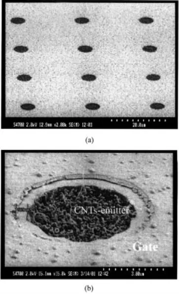
Fig. 2(a) shows the SEM micrograph of the fabricated de-vice arrays. The CNTs emitter layers were selectively deposited within the emitter areas. The gate aperture was 4 m in diam-eter. The field emission array contained 4 4 triode devices and the equivalent emitter area was approximately 200 m .
CHEN et al.: LOW TURN-ON VOLTAGE FIELD EMISSION TRIODES WITH SELECTIVE GROWTH OF CARBON NANOTUBES 517
Fig. 2. (a) SEM micrograph of the CNTs triode array. (b) SEM micrograph of the CNTs triode device.
Fig. 2(b) is the SEM micrograph of a single triode device. The interelectrode gap between gate and emitter formed by the wet etching process is about 0.6 m and no interconnection between the poly Si gate and CNTs was observed.
The fabricated device was characterized by an ultra-high vacuum measurement system and the environment was main-tained at 10 torr. The P22 phosphor coated ITO glass was applied as the anode. During measurement, the anode was set at 600 V and the distance between the anode and the CNTs triode array was about 450 m. The gate was kept at 50 V at poor vacuum for 10 min to evaporate the absorbents before measurement. Fig. 3 depicts the current-voltage (I-V) characteristics and the F–N plot of the low turn-on voltage CNTs triode array. The linearity of the F–N plot clarifies the field emission phenomenon. The turn-on voltage, defined as the voltage at which the F–N plot becomes linear, is 13 V. The emission current exceeds 23 A when the gate voltage reaches 60 V. Short-term reliability of the fabricated devices was also investigated. Fig. 4 reveals the stability of the emission current. The fluctuation was about 10% over 1800 sec when the gate voltage was set at 35 V.
Fig. 3. (a) Field emission current versus gate voltage, with anode was set at 600 V and (b) F–N plot of the fabricated device; the linearity clarifies the field emission phenomenon.
Fig. 4. The current fluctuation versus stress time as the gate voltage is set at 35 V.
IV. CONCLUSION
A CNTs based field emission triodes array with low turn-on voltage has been successfully fabricated. The CNTs emitter was selectively deposited on the patterned iron layers within the emitter area by MPCVD. The gate to emitter distance was well controlled by the wet etching process to avoid the short circuit problem between the gate and the CNTs emitter. Fabrication is an easily controllable, self-aligned, and well-established IC process. The field emission properties imply a low turn-on gate
518 IEEE ELECTRON DEVICE LETTERS, VOL. 22, NO. 11, NOVEMBER 2001
voltage of 13 V and an extremely high emission current of 23 A at 60 V. The emission current fluctuation was 10% over 1800 s. These excellent properties suggest that CNTs field emission triodes have potential in vacuum microelectronic applications and flat panel displays.
ACKNOWLEDGMENT
The authors would like to thank the Semiconductor Research Center of National Chiao Tung University for its technical sup-port.
REFERENCES
[1] P. G. Collins and A. Zettl, “A simple and robust electron beam source from carbon nanotubes,” Appl. Phys. Lett., vol. 69, pp. 1969–1971, 1996.
[2] Q. H. Wang, T. D. Corrigan, J. Y. Dai, and R. P. H. Chang, “Field emis-sion from nanotube bundle emitters at low fields,” Appl. Phys. Lett., vol. 70, pp. 3308–3310, 1997.
[3] J. M. Bonard, J. P. Salvetat, T. Stockli, W. A. de Heer, L. Forro, and A. Chatelain, “Field emission from single-wall carbon nanotube films,”
Appl. Phys. Lett., vol. 73, pp. 918–920, 1998.
[4] F. G. Tantair, L. C. Chen, S. L. Wei, W. K. Hong, K. H. Chen, and H. C. Cheng, “High current density field emission from arrays of carbon nanotubes and diamond-clad Si tips,” J. Vac. Sci. Technol. B, vol. 18, no. 3, pp. 1207–1211, 2000.
[5] K. Matsumoto, S. Kinosita, Y. Gotoh, T. Uchiyama, S. Manalis, and C. Quate, “Ultralow biased field emitter using single-wall carbon nanotube directly grown onto silicon tip by thermal chemical vapor deposition,”
Appl. Phys. Lett., vol. 78, no. 4, pp. 539–540, 2001.
[6] N. S. Lee, W. B. Choi, W. K. Yi, Y. W. Jin, Y. S. Choi, J. E. Jung, S. G. You, J. H. You, C. G. Lee, S. H. Cho, and J. M. Ki, “The carbon-nanotubes based field-emission displays for future large and full color displays,” in Microprocesses and Nanotechnol. Conf., 2000 Int., 2000, pp. 124–126.
[7] Q. H. Wang, M. Yan, and R. P. H. Chang, “Flat panel display prototype using gated carbon nanotube field emitters,” Appl. Phys. Lett., vol. 78, pp. 1294–1296, 2001.