國
立 交 通 大 學
電子工程學系 電子研究所碩士班
碩 士 論 文
未摻雜之氧化鋅薄膜電晶體的製作與特性分析
Fabrication and Characterization of Undoped-ZnO
Thin Film Transistors
研 究 生: 李信宏
指導教授: 林鴻志 博士
黃調元 博士
未摻雜之氧化鋅薄膜電晶體的製作與特性分析
Fabrication and Characterization of Undoped-ZnO
Thin Film Transistors
研 究 生: 李信宏
Student : Shin-Hung Li
指導教授: 林鴻志 博士
Advisors: Dr. Horng-Chih Lin
黃調元 博士
Dr. Tiao-Yuan Huang
國 立 交 通 大 學
電子工程學系 電子研究所碩士班
碩 士 論 文
A Thesis
Submitted to Department of Electronics Engineering & Institute of Electronics College of Electrical Engineering and Computer Engineering
National Chiao Tung University in Partial Fulfillment of the Requirements
for the Degree of Master of Science
in
Electronics Engineering July 2013
Hsinchu, Taiwan, Republic of China
i
未摻雜之氧化鋅薄膜電晶體
的製作與特性分析
研究生 : 李信宏 指導教授 : 林鴻志 博士
黃調元 博士
國立交通大學
電子工程學系 電子研究所碩士班
摘要
本篇論文中,我們利用反轉堆疊式薄膜電晶體的技術成功地製作出氧化鋅薄膜電晶 體。利用射頻濺鍍的方式製作氧化鋅薄膜,擁有製程溫度低、大面積均勻性佳等等的優 點。此外,因為反轉堆疊式結構的製程步驟簡單與低成本,讓我們能夠進行不同沉積條 件下的氧化鋅薄膜所造成的影響,其中包括氧氣流量、溫度控制和厚度控制。然後利用 適切的製程參數製作的氧化鋅薄膜電晶體做進一步的分析,例如自由電子在電晶體通道 裡產生的頻率響應。 此外,更進一步地討論氧化鋅薄膜電晶體的可靠度,包括了變溫量測、照光和電壓 測試。我們觀察到在持續加正電壓情況下,因為閘極介電層內有很多缺陷易抓住電子而 造成臨界電壓的正偏移;此外,我們也觀察到當有照光的情況下通道會產生很多的電子 電洞對,使元件受影響。ii
Fabrication and Characterization of Undoped-ZnO
Thin Film Transistors
Student : Shin-Hung Li Advisors : Dr. Horng-Chih Lin Dr. Tiao-Yuan Huang
Department of Electronics Engineering and Institute of Electronics National Chiao Tung University, Hsinchu, Taiwan
Abstract
In this thesis, we have successfully fabricated ZnO TFTs with the inverted-staggered
structure. RF sputter method, which has merits of low manufacture temperature and good uniformity on a large scale, was employed to deposit the ZnO films,. Because of the simple fabrication processes on inverted-staggered structure, we can investigate the impacts of various deposition conditions on the ZnO films, such as the oxygen flow rate, substrate temperature, and ZnO thickness. Finally, the ZnO TFTs fabricated with suitable manufacture parameters were investigated further. In addition to the I-V measurements, multi-frequency C-V characterization is also performed.
Subsequently, we also investigated the reliability of ZnO TFTs, including the dependence of measurement temperature, illumination and voltage stress. We observed obvious positive shift and little degradation of S.S. by the positive voltage stress, indicating that the shift is mainly caused by electron trapping in the gate dielectric. The effects of additional illumination were also explored.
iii
Acknowledgement
首先,我要特別感謝我的兩位指導老師,黃調元博士與林鴻志博士。黃老師總是很 有耐心的教導我們半導體物理與製程的觀念,且總是面帶笑容,讓學生相處起來不會有 太大的壓力,因而更能夠親近老師、勇敢地發問。而林老師在實驗上總是不吝嗇、絲毫 不苟的給學生指導和建議,讓我學習到做學術研究的精神並且感受到老師對學生和做研 究的熱情。兩位老師的態度總是能激勵學生積極向學,不僅僅在實驗方面而已,老師待 人處事的態度也讓學生受益良多,這些都將為學生以後進公司甚至未來生活帶來很大的 幫助。 接下來我要感謝實驗室的成員,因為他們的協助,讓我可以順利的完成實驗。第一 次做實驗帶領我的郭嘉豪和呂榮哲學長,無論是機台或觀念有不懂都會不厭其煩地主動 指導我,還有在討論實驗遇到的問題和現象,總是可以提出精闢的看法。此外,其他學 長姐,蔡子儀學長、林政頤學長、鐘嘉文學長、謝博璿學長以及李克慧學姊在我實驗遇 到困難時也會適時的幫助我,這些我也將銘記在心。且不僅僅是實驗上的幫助,在日常 生活中也充滿了許多歡樂和加油打氣,特別是呂榮哲學長,總是會號召實驗室成員一起 聚餐,聊天分享生活趣事。 在 631 的成員,由於維軒的實驗主題跟我很像,所以總是可以跟我討論實驗上的問 題,且適時地給我幫助和建議,讓我的實驗更能夠順利進行。湘婷經常帶一堆美食給大 家吃,讓我可以認識更多的美食。明鴻、靜玲、佳文、浩君、宇安都是我碩士生涯的夥 伴,大家一起努力,這些都是珍貴的回憶。還有後來加入的 628 的學弟妹以及 629 的管 金儀學長,你們的加入讓 ADTL 實驗室充滿了更多的歡樂和回憶。iv
CONTENTS
Abstract (Chinese)………...….i
Abstract (English) ………..ii
Acknowledgement………..iii
Contents………...………iv
Table Captions……….………...vi
Figure Captions………..vi
Chapter 1 Introduction………..………
1
1.1 General Background of Metal-Oxide Based Thin-Film Transistors
(TFTs)……….1
1.2 Properties and Conductive Mechanisms of ZnO………...2
1.3 Motivation……….4
1.4 Organization of this Thesis………..5
Chapter 2 Device Fabrication, Measurement Setup and
Parameter Extraction……….6
2.1 Device Fabrication and Process Flow……….6
v
2.3 Source/Drain Series Resistance………...8
2.3.1 Metal-Semiconductor Contacts………..8
2.3.2 Parasitic Series S/D Resistance……….……..9
2.3.3 Comparison of Junctionless, Accumulation and Inversion mode.10
Chapter 3 Results and Discussion………
…...
11
3.1 Properties of ZnO………...11
3.2 Extraction of Density of States (DOS) with Multi-Frequency C-V
Measurements……….12
3.3 Effects of Different Deposition Conditions…
…………...15
3.3.1 Effects of ZnO Thickness (
𝑻
𝒁𝒏𝑶)………..
15
3.3.2 Effects of Deposition Temperature………...15
3.3.3 Effects of Oxygen Flow………
…………..16
3.4 Reliability………
………….17
Chapter 4 Conclusions and Future Work………...20
4.1 Conclusions……….…….20
4.2 Future Work………21
References………..22
Tables………..27
vi
Table Captions
Table 1.1
Comparison
of
amorphous-Si:H
(a-Si:H),
poly-Si
and
metal-oxide TFTs [13]……….27
Table 3.1
Hall
measurement
results
for
films
with
following
fixed
deposition
parameters:
RF
power
=
100
W, Ar flow = 50 sccm
and chamber pressure = 5 mTorr………...28
Figure Captions
Chapter 1
Fig. 1.1 The
hexagonal
wurtzite
structure
of
zinc
oxide.
O
atoms
are
represented
by
the
larger
white
spheres
and Zn
atoms
are
the
smaller black spheres [2]………...29
Fig. 1.2 The rock salt (left) and zicblende (right) structures of zinc oxide. O
atoms are the larger white spheres and Zn atoms are smaller black
sphere [2]………29
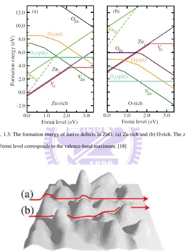
Fig. 1.3 The formation energy
of native defects in ZnO; (a) Zn-rich and (b)
O-rich.
The
zero of
Fermi
level
corresponds
to the
valence-band
maximum [18]……….30
vii
Fig. 1.4 Illustration of percolation model. (a) An electron chooses a shorter
but
higher
barrier path.
(b)
An electron chooses
a longer, but lower
barrier path [19]……….30
Chapter 2
Fig. 2.1 (a)
A
3-dimentional
schematic
and (b)
a
cross-sectional
schematic
of the process after gate electrode definition………...31
Fig. 2.2 A cross-sectional
schematic (a) after
photoresist pattern
formation
and (b) the subsequent Al deposition………31
Fig. 2.3 (a) A
3-dimentional
schematic
and (b)
a cross-sectional schematic
of the device after S/D definition………..31
Fig. 2.4 (a) A
3-dimentional
schematic
and (b) a cross-sectional schematic
of
the
complete
device
structure
with
defined
channel length
(L)……….31
Fig. 2.5 (a)
Parallel-
(b)
and series-version,
and
(c)
complete
equilavent
circuit of TFTs devices………...32
Fig. 2.6 Band
diagrams
of
metal-semiconductor
contacts
(a)
under
zero
bias
and
(b)
forward biased
with
a voltage (
𝑽
𝒂) applied on metal
[31]………32
Fig. 2.7 Major resistance components in (a) conventional MOSFET and (b)
inverted-staggered
tpye
TFTs,
both
showing the physical channel
length
L,
effective
channel
length
𝑳
𝒆𝒇𝒇= 𝑳 − ∆𝑳
and
viii
Fig. 2.8 An
intersection
point
is
obatined
in
the
𝑹
𝒎− 𝑳
plots
of
conventional MOSFETs [28]……….33
Fig. 2.9 No
intersection point is observed
among the
𝑹
𝒎− 𝑳 plots
of the
IGZO TFTs [32]………..34
Fig.
2.10 Comparison of transfer characteristics of junctionless,
inversion-mode, and accumulation-mode transistors…………34
Chapter 3
Fig. 3.1 The XPS spectra of O 1s for sample A in Table 3.1………...35
Fig. 3.2 The XPS spectra of O 1s for sample B in Table 3.1………...35
Fig. 3.3 The XPS spectra of O 1s for sample C in Table 3.1………...36
Fig. 3.4 The XPS spectra of O 1s for sample D in Table 3.1………...36
Fig. 3.5 The XRD spectra for sample A in Table 3.1………...37
Fig. 3.6 The XRD spectra for sample B in Table 3.1………...37
Fig. 3.7 The XRD spectra for sample C in Table 3.1………...38
Fig. 3.8 The XRD spectra for sample D in Table 3.1………...38
Fig. 3.9 The XRD spectra for sample E in Table 3.1………...39
Fig. 3.10 The XRD spectra for sample F in Table 3.1……….39
Fig. 3.11 TEM image showing the granular structure of ZnO (the black
regions)………...40
ix
Fig. 3.12
versus
plots of a ZnO TFT measured under different
frequencies……….40
Fig.
3.13 The transfer characteristics of a TFT at
and 1 V….41
Fig.
3.14 The band diagram of ZnO TFTs when the gate bias is (a) below
and (b) above threshold condition [22]………41
Fig.
3.15 The equivalent circuits of the ZnO TFT: (a) with the
frequency-dependent components (
and
); (b) without
the frequency-dependent
components……….42
Fig. 3.16 The C-V characteristics of a device under frequency of 100, 1k,
5k and 10k
Hz………42
Fig.
3.17
The extracted gate capacitance after de-embedding of the
frequency-dependent
components………...43
Fig. 3.18 DOS
and
as a function of
……….43
Fig. 3.19
The
versus
plot for oxygen flow = 1 sccm…….44
Fig. 3.20
Transfer characteristics and field-effect mobility………44
Fig. 3.21 Transfer characteristics of TFTs
with various
…………..45
Fig.
3.22
C-V
characteristics
for
various
under 100 Hz
condition……….45
Fig.
3.23
Transfer
characteristics of devices with various deposition
temperatures………..46
x
Fig. 3.24
Hall measurement results of ZnO films as a function of deposition
temperature.
Insets show the corresponding transfer curves…46
Fig.
3.25
The hysteresis of devices with channel deposited at room
temperature
and 200
, respectively……….47
Fig. 3.26
The XRD analysis of the two ZnO films deposited at 25 and 200
o
C,
respectively………47
Fig.
3.27
The transfer characteristics of devices with various oxygen flow
conditions……….48
Fig. 3.28
The
versus
plot for the device with oxygen flow =
9
sccm………48
Fig.
3.29
The band diagram of ZnO TFTs under off-state condition
(
)………49
Fig.
3.30
The band diagram showing the stage as the Fermi level at the
interface
reaches
around
the peak of DOS………..49
Fig.
3.31
The transfer characteristics of devices before (fresh) and after
PBS for 1, 100, 500 and 1000 seconds………50
Fig.
3.32
Transfer characteristics of devices before (fresh) and after NBS
for 1, 100, 500 and 1000 seconds………50
Fig. 3.33
Transfer characteristics of devices before (fresh) and after NBLS
for 1, 100, 500 and 1000 seconds
……….51
Fig. 3.34
Transfer characteristics of devices before (fresh) and after PBLS
xi
Fig.
3.35
Transfer characteristics of a device measured at 25, 50, 75, 100
and 125
………52
Fig. 3.36
Transfer
characteristics
of
a
device
measured
at
25
and
125
………...52
Fig.
3.37
Transfer characteristics under measurement temperatures of 50,
1
Chapter 1
Introduction
1.1 General Background of Metal-Oxide Based Thin-Film
Transistors (TFTs)
Oxides have been an important part of electronic products for generations. They had played a key role as insulators, but now they have been technologically studied as semiconductors. One of the most popular materials is zinc oxide (ZnO) which has been studied widely a few years ago [1-5] because of many advantages the material exhibits, such as wide bandgap, large exciton binding energy, good piezoelectric properties, transparency, and so on. A number of methods are available for preparing ZnO, such as pulse laser deposition (PLD) [3], atomic layer deposition (ALD) [4] and radio-frequency (RF) magnetron sputter [5]. However, various preparation methods bring about distinctive device characteristics. Annealing [6] and surface passivation [7] have also been studied and proposed to be useful for improving the device characteristics.
The innovation of active-matrix liquid crystal display (AMLCD) has sprouted the TFT technology, even though TFT was conceptualized many years ago. Recently metal-oxide based TFTs, such as In-Ga-Z-O (IGZO), In-Z-O (IZO), ZnO, have been regarded as potential candidates to be used in AMLCD and active-matrix organic light emitting diode (AMOLED) [8-10]. While metal-oxide TFTs exhibit excellent electrical performance comparable to that of poly-Si TFTs, they could be much more attractive since they could be fabricated at low temperatures. Another characteristic feature of the metal-oxide TFTs is the low off-current as
2
compared with the state-of-the-art low-temperature poly-silicon (LTPS) technology. Actually the application of metal-oxide TFTs is not limited to the display territory. For example, it has been reported recently that this active device technology can be embedded in Cu-interconnects of an IC for building on-chip high-voltage control and I/O circuit blocks [11-12]. Without doubt, there are still lots of applications of zinc oxide, such as varistor, gas sensor, and solar cells. Table 1.1 [13] lists a performance comparison between metal-oxide, poly-Si and a-Si:H TFT technologies.
1.2 Properties and Conductive Mechanisms of ZnO
ZnO belongs to II-VI compound semiconductor and it has a hexagonal wurtzite lattice structure, as illustrated in Fig. 1.1 [2]. In general, one Zn ion (𝑍𝑛2+) is surrounded by
tetrahedron oxygen ions (𝑂2−) and they form an especial polarity which affects lots of
properties of ZnO. However, in an ideal wurtzite structure, the crystal geometry parameters c/a and u in a primitive cell are about 1.593 and 0.3856, respectively [14]. In addition to wurtzite structure, ZnO also exhibits cubic zincblende and rocksalt (NaCl) structures under specific conditions, as shown in Fig. 1.2 [2]. In solid-state physics, the basic interactions in metal oxides are usually between metal-d orbitals (𝑀𝑑) and overlapping 2p orbital (𝑂2𝑝) [15].
Another concept is, if the metal-oxide exists as imperfect crystal structure, in due course it will behave as a semiconductor. In other words, defects play a key role in affecting the semiconductor properties of metal-oxides. However, to optimize the performance of ZnO-based devices, basic physics of ZnO must be accurately explored. In spite of previous studies on native defects, such as first-principle study of native point defects in ZnO [16] and energetic native defects in ZnO [17], controlling the electrical conductivity of zinc oxides still remains as a main challenge. In general, two components of native point defects, which are donor like and acceptor like, can be objectively separated. By means of previous studies, the
3
defects include vacancies, interstitials, and antisites. Most investigations suggest that oxygen vacancies and zinc interstitials are the sources of n-type conductivity. On account of thermal-dynamic theory illustrated in Fig. 1.3 [18], the oxygen vacancies and zinc interstitials are abundant in ZnO. This is the reason that intrinsic zinc oxide is n-type semiconductors and the native defects contained inside will almost dominate the conduction of zinc oxide. Thus, changing the oxygen level, which is controlled by anthropogenic sources, can manipulate the electrical conductivity of the material. Oxygen level changes may be seen as an advantage of flexibility but at the same time it may also cause an unexpected variation in properties. Another disadvantage is that it’s difficult to form p-type ZnO because of the action of the native defects described above.
Studies on metal-oxide TFTs have shown interesting concepts in conductive mechanisms. For example, the percolation model [19] is a new way to reinterpret the conductive mechanism of amorphous-metal-oxide. The fundamental physical concept of percolation model is that there are different electron conduction paths, and it further assumes that fluctuated potential barriers are present in the amorphous-metal-oxide, resulting in a number of conduction paths, as illustrated in Fig. 1.4. Nevertheless, because zinc oxide is apt to form polycrystalline phase, the presence of grain boundary barrier modulation in ZnO [20] is another way to analyze the conductive mechanism. For simplicity, assuming a single grain boundary and the defect states are interpreted by a Gaussian distribution expressed as [20]
( ) { ( − )2}, (Eq. 1-1)
where ( ) and are the density of defect states and trap states, respectively, is the trap energy inside the band gap, and 2 are the peak energy and decay energy, respectively. The linear region of transfer curve of a device can be roughly described by the following equation:
4
where 𝑑 is the drain current, W, L and are channel width, length and geometry capacitance, respectively. , 𝑑 and are gate bias, drain bias and threshold voltage of the transistor, respectively. The grain-boundary model succeeds in explaining the mobility changes with gate bias and a wide range of drain current characteristics [20]. Furthermore, an exponential term ( ) where is the energy barrier in the grain boundary, can be added to the drain current equation in order to achieve a more accurate prediction. More recently, extraction of the density of states (DOS) is employed to explore the operation of the devices [21-27], and parts of them adopting conductance method which has been published in early days [28]. The concept is that sub-gap states can also influence the conduction mechanism by changing the surface potential. No matter what concept is, partially distinctive information is obtained from the analysis. In this thesis, study on the conductive mechanisms of ZnO TFTs is one of our objectives and in Chapter 3 we present and characterize our experimental results to address this issue in detail.
1.3 Motivation
According to the superior performance reported and confirmed in the literature, metal-oxide based TFTs show a large potential to substitute silicon-based TFTs in practical manufacturing. Actually, it’s very likely to bring the display industry to another climax. In the future, other applications would also be benefitted from the innovation of metal-oxide TFTs. Nonetheless, more accurate understanding of the operation principle and experimental observations are urgently requiring innovation. In this thesis, we have chosen ZnO as the channel material of the fabricated devices, due to its high carrier mobility and potentially cheaper cost as compared with IGZO which contains the rare and expensive indium. In another side, we used RF sputter as ZnO deposition method because it is more versatile than chemical vapor deposition (CVD) and can be processed at a low temperature. Furthermore, by
5
varying the ZnO deposition conditions, we can compare and study the effects of various factors. Since this is the first work on ZnO TFTs in our groups, we also intend to optimize the process parameters.
1.4 Organization of this Thesis
In this chapter we briefly review the history of ZnO TFTs. In Chapter 2 we will describe the fabrication and process flow of n-type ZnO TFTs. Another portion is measurement setup and some characteristics which are cause of fabrication. In Chapter 3 we will discuss fruitful experimental results by using various physical models and mathematic tools. Finally, we will give conclusions and suggestions for future works based on our experimental results.
6
Chapter 2
Device Fabrication, Measurement Setup and
Parameter Extraction
2.1 Device Fabrication and Process Flow
In this thesis, we use an inverted-staggered type structure which is one of the commonly-used TFTs in display industry due to its simple fabrication processes [29]. The complete fabrication processes only need four photolithography masks: gate electrode, source and drain (S/D), active area, and metal contact definition. The 3-dimensional and cross-sectional views of the fabricated ZnO TFT are shown in Figs. 2.4 (a) and (b), respectively. The detailed processes are as follows. First, Si wafers were oxidized in a horizontal furnace to simulate glass substrates for display industry. Second, a 200-nm-thick Al-Si-Cu film was deposited by physical vapor deposition (PVD) and then patterned by photolithography and wet etching to form gate electrode, as shown in Fig. 2.1. Third, a silicon dioxide (20 nm) was deposited by plasma-enhanced chemical vapor deposition (PECVD) as the gate dielectric. Fourth, a ZnO film was deposited by RF magnetron sputter as the channel layer. It should be noted that the ZnO target, which is composed of sintered ZnO powders, needs a pre-sputtering treatment prior to the deposition in order to remove the otiose particles. More importantly, the deposition conditions for the channel layers, such as oxygen flow rate, pressure, deposition temperature, and time are the key to the electrical characteristics of devices. Therefore, we intentionally explore the impacts of deposition conditions on their characteristics in Chap. 3. Moreover, in Sect. 3.1, we specially give material analyses on the deposited ZnO films before we discuss our experimental results of the ZnO TFTs. Fifth, the photo-resist was spin-coated, exposed, and developed to define the S/D regions, as illustrated
7
in Fig. 2.2 (a). Then, a 300-nm-thick Al layer was deposited by thermal coater as shown in Fig. 2.2 (b). Subsequently, the devices were immersed in a tank paired with ultrasonic oscillator to peel off the photo-resist. The S/D area appeared after the lift-off process which can suppress the damages induced on the channel surface. The active area was defined by standard photolithography and then etched by diluted hydrochloric acid (HCl), as illustrated in Figs. 2.3 and 2.4, in which the definitions of physical channel length (L) and channel width (W) were also described. Finally, the metal contact of gate was defined.
2.2 Measurement Setup
The typical current-voltage (I-V) electrical parameters are measured by an HP4156A precision semiconductor parameter analyzer, and the basic parameters of the ZnO TFTs, including sub-threshold swing (S.S.), threshold voltage ( ), field effective mobility ( 𝐹 ) and so on are also extracted. At the same time, the capacitance-voltage (C-V) electrical parameters are measured by an Agilent 4284 precision LCR meter. This method is capable of resolving a number of behaviors of the charges contained in the devices. When the charges are varied with the time-dependent electric field, it produces a displacement current [30]. Subsequently, capacitance C relates the displacement current i to the voltage V, and is defined as
𝑖 𝑑𝑉𝑑 (Eq. 2.1) or
𝑑𝑄𝑑𝑉. (Eq. 2.2)
Furthermore, the C-V characteristics are evaluated by the multi-frequency C-V method in order to extract the density of states (DOS) and understand the behaviors of the charge in responses to the frequency. The frequency of the measurements is varied between 60 Hz-100 kHz. The gate and S/D are connected with high-terminal and low-terminal,
8
respectively, as shown in Fig. 2.4(a). The equivalent circuit of basic model includes the device elements and an output resistor, which is due to the parasitic series S/D resistance ( ). The equivalent circuit of ZnO TFTs can be represented by the parallel channel resistance ( ), capacitance ( ) in series with the geometry capacitance ( ) and , as shown in Fig. 2.5(c). The circuit can be transformed to either parallel or series connection, as shown in Figs. 2.5(a) and (b), respectively. The parameters ( , , , and ) of the equivalent circuit of the ZnO TFTs can be extracted by numerical calculation.
2.3 Source/Drain Series Resistance
The metal-semiconductor contacts formed over the S/D regions are crucial for the parasitic . Moreover, the ZnO TFTs are similar to junctionless or accumulation mode transistors owing to the n-type doping nature of the material. The conduction mechanisms are discussed briefly in sub-section 2.3.3.
2.3.1 Metal-Semiconductor Contacts
The metal-semiconductor contacts are an important element in affecting the output characteristics of the fabricated devices. Here, we briefly discuss the operation of the metal-semiconductor contact, which is also called Schottky diodes. From Fundamentals of
Modern VLSI Devices [31], the band diagram of the metal-semiconductor can be described in
Fig. 2.6(a). When surface states are ignored, the barrier height of electrons (𝑞𝜑𝐵𝑛) is
𝑞𝜑𝐵𝑛 𝑞(𝜑𝑚 𝜒), (Eq. 2.3) where 𝑞φ𝑚 and qχ are the metal work function and the electron affinity of semiconductor, respectively. When the system is in thermal equilibrium with zero bias, the built-in potential 𝜑 𝑖 is
9
where 𝑐 and are conduction band minimum and quasi Fermi-Level, respectively. When we apply a positive bias on metal, there is a net flow of thermic electrons from semiconductor into metal, as illustrated in Fig. 2.6(b). According to the above illustration, the is an important factor affecting 𝑞𝜑𝐵𝑛 which is also related to the carrier concentration in the semiconductor. If the semiconductor has a higher carrier concentration, the Schottky diodes behave like an ohmic contact.
2.3.2 Parasitic Series S/D Resistance
In this sub-section, we introduce the extraction of the based on the scheme reported in literatures [28] and [32]. As shown in Fig. 2.7(a), for conventional MOSFETs the total resistance ( 𝑚 𝑑 ⁄ ) of the device can be written as 𝑑
𝑚 𝑐 + 𝜇 −∆
𝑒𝑓𝑓 𝑜𝑥(𝑉𝑔−𝑉𝑡ℎ)+ (eq. 2.5)
where is field effective mobility, is gate bias, is threshold voltage, and 𝑐 is channel resistance, respectively. L is the physical gate length and ΔL is the extent of reduction in channel length due to the formation of S/D junctions, and thus L-ΔL represents the effective channel length, 𝐿 . Although with a structure distinctly different from the
conventional one, 𝐿 of inverted-staggered structure can still be defined as illustrated in Fig. 2.7(b). However, it should be noted that 𝐿 of inverted-staggered type is determined by the mask. For simplicity, the 𝑚 can be written as
𝑚 𝜇 𝑒𝑓𝑓
𝑒𝑓𝑓 𝑜𝑥(𝑉𝑔−𝑉𝑡ℎ)+ . (eq. 2.6)
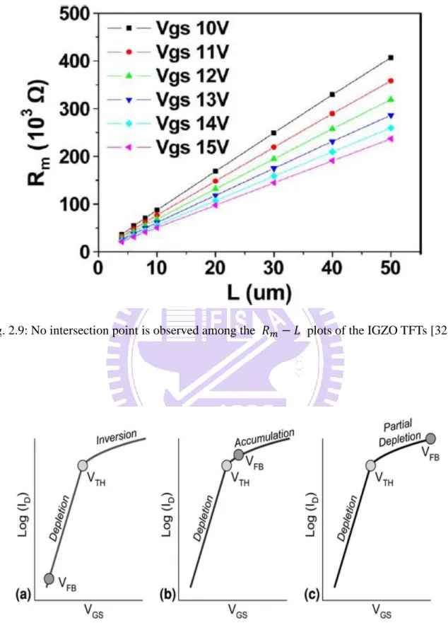
Sometimes, unlike the case of conventional MOSFETs that 𝑚-𝐿 lines have a common intersection point, as shown in Fig. 2.8 [28], the 𝑚-𝐿 lines fail to intersect at a point due to the lower carrier concentration, with an example shown in Fig. 2.9 [32]. When this happens -dependent can be determined by
𝑚 𝑐 + 𝐵 + 𝐴 𝐿 (eq. 2.7)
10
The can be used in the scheme of DOS extraction employed in Chap. 3.
2.3.3 Comparison of Junctionless, Accumulation and Inversion mode
Recently, the junctionless transistor has received much attention because it is compatible with the CMOS fabrication and offers a few advantages over the inversion-mode devices, like the elimination of junction formation process [33]. To distinguish the differences between the device operation, the transfer curve of the three types of SOI MOSFETs: inversion-mode, accumulation-mode and junctionless transistors, as shown in Fig. 2.10 in which the flat-band voltage ( ) is labeled. From the figure it is seen that the of the inversion-mode devices
is obviously below V . For accumulation-mode devices, is slightly above V , and is much larger than in the case of junctionless devices. Thus, and carrier concentration are very important in determining the type of the device and its operation mode.
11
Chapter 3
Results and Discussion
3.1 Properties of ZnO
Pure ZnO films deposited under various deposition conditions are studied in order to understand the basic material properties which are important for the device characteristics. In this section, several characterization methods, including X-ray Diffractometer (XRD), X-ray photoelectron spectroscopy (XPS) and Hall Measurement, are presented.
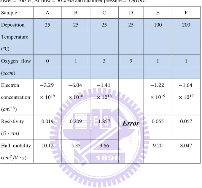
Hall measurement: In the measurements a silicon dioxide as a high resistance buffer layer is
needed in order to prevent inevitable noises. Another note is that indium balls are adhered to the measured ZnO films for reducing the contact resistance. The results of five splits (sample A-F) of different deposition conditions, including various oxygen flow and substrate temperature, are presented in Table 3.1. The information about carrier concentration, resistivity and bulk mobility are shown in Table 3.1, too. The increase in electron concentrations at the small oxygen flow condition is reasonable because more oxygen vacancies are expected to be contained in the film. In the study we found that the measurement failed for the sample D prepared under the oxygen flow of 9 sccm because the resistivity is too large to be measured. However, the electron concentration seems not to increase with increasing temperature. Effects of this finding on the transfer characteristics of ZnO TFTs are discussed in Sect. 3.2.3.
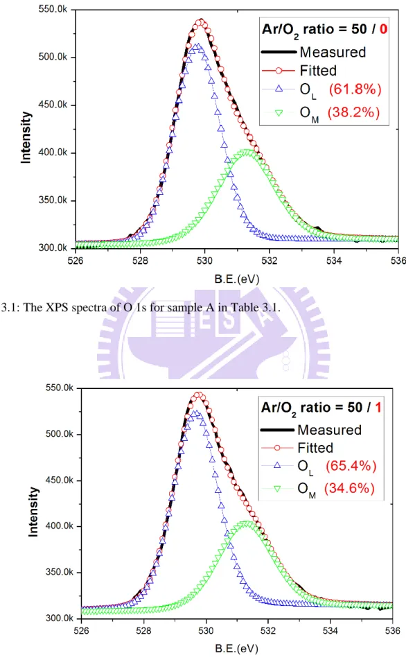
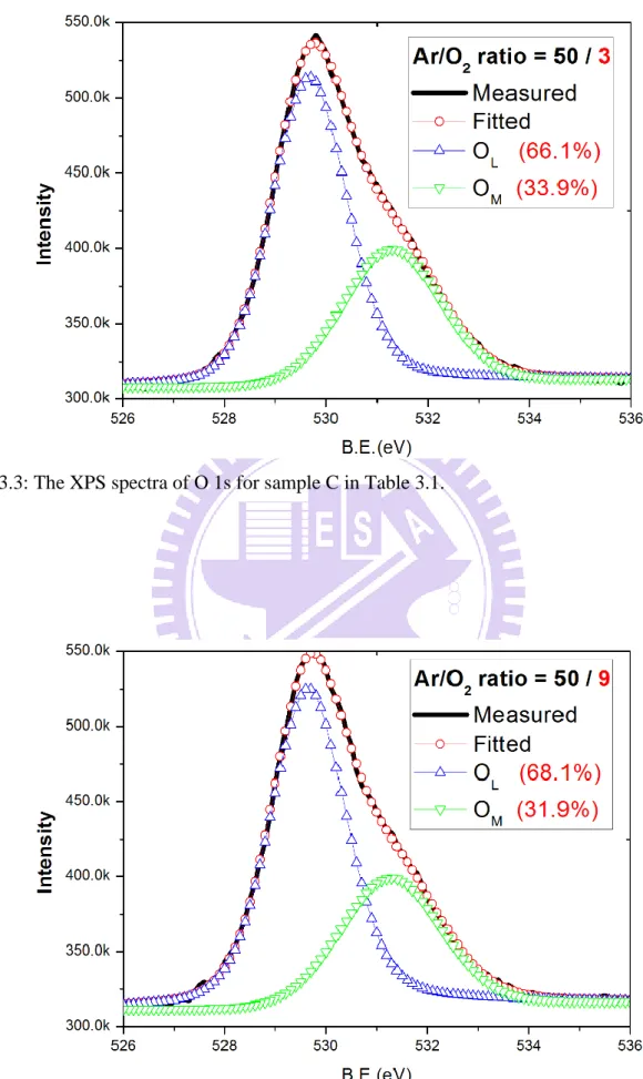
X-ray photoelectron spectroscopy: XPS was used to identify the chemical state of IGZO
films in previous work [34-35]. According to the literature [35], O 1s peak could be fitted by three waves, centered at 530.06, 531.56 and 532.62 eV, respectively. The low binding energy
12
associated with the magnitude of oxygen vacancies. The high binding energy OH is associated
with the weak bound oxygen on the surface of ZnO films, such as adsorbed H2O or O2. For
simplicity, we assume the influences of environment on various ZnO films are identical and negligible. Thus, the XPS spectrum were fitted by two waves, including OL and OM. Figs.
3.1-3.4 show the XPS spectrum of O 1s peak under various oxygen flow conditions, and they indicate that the Gaussian-fitted results fit the experimental data. The ratio ( 𝐴𝑀
𝐴𝐻+𝐴𝑀), where AM
and AH are the sum of the intensity areas of OM and OL, respectively, increases when ZnO film
was deposited under a higher oxygen flow condition. The observed trend is consistent with the experimental results of Hall Measurements that the carrier concentration decreases with increasing oxygen flow.
X-ray Diffractometer: The XRD patterns of ZnO films with various deposition conditions are
shown in Figs. 3.5-3.10. These results show that the ZnO films are highly textured with c-axis (002), and the observed peaks are nearly the same among the test samples regardless of the various deposition conditions. Moreover, the coherently diffracting domain size can be calculated by Scherrer’s equation [36]. Grain size is estimated to be in the 5~10 nm range which is in agreement with the results of transmission electron microscopy (TEM), as shown in Fig. 3.11.
3.2 Extraction of Density of States (DOS) with
Multi-Frequency C-V Measurements
In this section, we discuss the effect of varying frequency on the C-V curves and the extraction of DOS in the bandgap of the ZnO film based on the C-V results. Although varying the frequency of the applying basically does not change the equivalent circuit of devices, the components in the circuits, including capacitance and resistance, depend on the frequency. Fig. 3.12 shows the measured capacitance-V characteristics of a device under various
13
frequencies. Fig. 3.13 shows the transfer characteristics at 𝑑 0.1 and 1 V. The device’s L and W are 50 and 300 μm, respectively. The deposition conditions of the ZnO channel are the same as those of the sample B shown in Table 3.1. It is seen in Fig, 3.12 that the measured capacitance (Cm) becomes independent of the applied gate bias as the frequency is too high,
implying the charges contained in the device are not responsible to the change of the small-signal frequency. Compared with the conventional MOSFETs, the channel resistance of the thin oxide channel is huge so the frequency repose of the devices is significantly affected. Note that the C-V curves overlap each other under the lower frequency conditions (e.g., 60, 80 and 100 Hz), as shown in Fig. 3.12.
The multi-frequency C-V characterization allows us to extract the DOS in the bandgap [21-23]. When the localized states are below the quasi Fermi level, they prefer to be occupied by electrons. When they are close to 𝑐, the electrons contained in the localized states are likely to be released into the conduction band. By the same token, the valence-band electrons are likely to be trapped into the localized traps when they are close to the valence band edge. Figs. 3.14(a) and (b) illustrate the charge transfer processes between these states occurring as
Vg is smaller and larger than Vth, respectively. However, these behaviors (capture and emission)
also need time to trigger and would draw consequence on the C-V measurements. A simplified C-V equivalent circuit accounting for the above description is illustrated in Fig. 3.15(a) which includes resistance and capacitance related to localized states ( ) and capacitance due to free electrons ( 𝐹 ). If the frequency-dependent components, namely, and , can be extracted and de-embedded from the circuit, then the circuit is
modified as that shown in Fig. 3.15(b). In this figure the frequency-independent effective capacitance is denoted as Cg. The can be determined by 𝑚-vs.-𝐿 plot illustrated in
Sect. 2.3.2. The detailed processes about acquiring the Cg-vs.-Vg characteristics from the
multi-frequency C-V measurements are given in the references [21-23]. To verify the above concept, Fig. 3.16 shows the 𝑚 of the ZnO TFTs under four frequencies (100, 1k, 5k and
14
10k Hz). Based on the measured results and the procedure proposed in references [21-23], was calculated with three elements ( 𝐹 and ) and the results are shown in Fig. 3.17. Note that three different combinations of the frequencies show the same characteristics, verifying that the method is useful for eliminating the influences of frequency-dependent component. Then, the DOS can be determined as follows [22]:
𝑔𝐴 𝑉 𝑙 𝑚 𝑑𝑄 𝑑 𝑉 𝑙 𝑚 𝑞𝑑𝑄 𝑑𝑉 𝐿𝑂𝐶
( × ×𝑇𝑍𝑛𝑂)×𝑞 (eq. 3.1)
The DOS or the density of the localized states (𝑔𝐴 ) and the free electron density (𝑛 𝑟 )
versus are plotted in Fig. 3.18. The free electron density is in the 10 7~10 8 𝑐𝑚−3 range which is typical in the ZnO TFTs and is consistent with the enhancement-mode transfer characteristics shown in Fig. 3.13. One difficulty associated with such scheme is that it is hard to precisely determine the flat-band voltage ( ). For simplicity, an energy level is
defined at a specific current 𝑑 1 × 10− 3 (A) instead of ( ). Vg corresponds to the specific current level is denoted as . Note that is expected to be close to . Then, the energy distribution of the 𝑔𝐴 can be expressed as a function of the energy level E within the gap:
( ) ∫ (1 𝑔 𝑜𝑥)
𝑉𝑔
𝑉 (eq. 3.2)
and the results are shown in Fig. 3.19. Within the context of DOS and I-V transfer characteristics, the primary conduction mechanism of ZnO TFTs is similar to that of an accumulation-mode device because of the relatively low 𝑛 𝑟 . The field-effect mobility 𝐹 increases when a positive is applied, as shown in Fig. 3.20.
15
3.3 Effects of Different Deposition Conditions
3.3.1 Effects of ZnO Thickness (𝑻𝒁𝒏𝑶)
The influences of channel thickness, 𝑇𝑍𝑛 , are studied in this sub-section by characterizing the I-V transfer characteristics of ZnO TFTs with 𝑇𝑍𝑛 of 25, 40 and 55 nm. These channel films were deposited with RF power of 100 W, substrate temperature of 25℃, chamber pressure of 5 mTorr and Ar/O2 ratio of 50/1. The device L and W are 50 and 300 μm,
respectively. Obviously negative shift and slight degradation in S.S. with increasing 𝑇𝑍𝑛 are observed in Fig. 3.21. Thicker 𝑇𝑍𝑛 has more electrons in the channel, resulting in a higher conduction current at a specific gate bias. Moreover, the C-V plot in Fig. 3.22 for the one with 𝑇𝑍𝑛 -55nm is found to continuously decrease with decreasing gate voltage in the negative bias regime. The following equation,
𝑚 𝑜𝑥+ 𝑑𝑒𝑝, (eq. 3.3)
where 𝑚 and 𝑑 𝑝 are the measured capacitance and depletion capacitance, respectively, can be employed to explain the mechanism. Theoretically 𝑚 will reach a minimum as the gate bias is adequately negative so that the channel is fully depleted. For the case with 𝑇𝑍𝑛 of 55nm, obviously the channel is too thick to be fully depleted in the gate voltage range applied in the figure. Thus, the series 𝑑 𝑝 tends to further lower 𝑚 in the negative voltage regime. Note that S.S. is also influenced by 𝑇𝑍𝑛 due to the higher amount of the charges in the channel depletion region.
3.3.2 Effects of Deposition Temperature
A rise in the deposition temperature is usually expected to promote the electron mobility in the deposited ZnO because of the better crystallinity. To explore the effects of temperature, parameters of the deposition conditions except temperature are fixed. They are 𝑇𝑍𝑛 of 15 nm, RF power at 100 W, chamber pressure at 5 mTorr and ratio of Ar/O2 at 50/1. The device L
16
and W are 50 and 400 μm, respectively. Fig. 3.23 compares transfer characteristics of devices subjected to three various temperatures: 25, 100 and 200 ℃. It is seen in the figure that high temperature conditions cause a negative shift in and the S.S. degradation. The appearance of the shift is believed to be due to the increase in the electron concentration under the high temperature deposition condition as confirmed by the Hall Measurement. Fig. 3.24 shows that the electron concentration increases with increasing deposition temperature. Furthermore, Fig. 3.25 shows the hysteresis phenomenon of the two devices deposited at 25 and 200 oC, respectively. Under the room temperature condition, the hysteresis is obvious, implying that abundant defects are contained in the channel. As the temperature is raised to 200 oC, the hysteresis becomes negligible. Promotion in the crystallinity is postulated to be responsible for such an observation. Fig. 3.26 shows the intensity versus angle (2θ) of the ZnO films deposited at 25 and 200 oC, respectively. The larger intensity of the c-axis (002) signal seen in the latter indicates that the ZnO film deposited at 200 oC has better crystallinity.
3.3.3 Effects of Oxygen Flow
To optimize the electrical characteristics of ZnO TFTs, we need to carefully control the oxygen levels because the changes from Zn- to O-rich condition would cause different characteristics of ZnO TFTs. Except the oxygen flow, all other parameters of the ZnO deposition conditions are fixed, including 𝑇𝑍𝑛 of 15 nm, RF power at 100 W, chamber pressure at 5 mTorr and ratio of Ar/O2 at 50/1. The device L and W are 50 and 300 μm,
respectively. Fig. 3.27 shows the transfer characteristics of the devices with the ZnO channel deposited at various oxygen flows, including 1, 3 and 9 sccm. Based on a previous work [18], the oxygen vacancies are the source of n-type conduction carriers. Increasing the oxygen flow is thus expected to reduce the free carrier concentration which is essential for conduction of enhancement-mode devices. Fig. 3.27 shows indeed that the transfer characteristics have a positive shift when the oxygen flow increases. The cause of the positive shift is believed
17
to be due to a reduction in the oxygen vacancies in the ZnO films. XPS results shown in Figs. 3.2-3.4 confirm the behavior. However, a positive shift of with a hump effect is also observed for the device with oxygen flow of 9 sccm. In order to investigate the source of such a hump, the DOS (𝑔𝐴 ( )) in the energy gap of the ZnO channel were extracted by
multi-frequency C-V method presented in Sect. 3.2. 𝑔𝐴 ( ) versus is plotted in Fig. 3.28 for the device with oxygen flow of 9 sccm. In this figure E1 is the level
corresponding to Vg =0.4 V. As shown in Fig. 3.28, a peak at 1.5 𝑒 is clearly
observed. Band diagrams are illustrated in Figs. 3.29 and 30 to facilitate the understanding of the hump phenomenon. Fig. 3.29 is the band diagram in the off state (say, 𝑑 3.3 × 10− 4 A at 0.4 V), the states existing below were occupied by electrons. As shown in Fig. 3.30, the hump occurs as the surface potential is crossing the peak of 𝑔𝐴 ( ). The high amount of defects slows down the movement of surface potential with increasing and thus the S.S. is degraded. The result indicates that the ZnO films were changed to O-rich condition under the high oxygen flow conditions, as has been pointed out in a previous work [18]. Fig. 1.3 (b) shows that the formation energy of the oxygen interstitials (𝑂𝑖) and zinc vacancies ( 𝑍𝑛) are lower than the other species shown in the same figure, resulting in more defect states
formed (𝑂𝑖 and 𝑍𝑛). These defects are speculated to be responsible for the appearance of peak in 𝑔𝐴 ( ).
3.4 Reliability
In this section, we investigate instabilities of positive bias stress (PBS), negative bias stress (NBS), positive bias light stress (PBLS), negative bias light stress (NBLS) and the temperature dependence on ZnO TFTs. Fig. 3.31 shows the transfer characteristics of the devices subjected to PBS, NBS, PBLS and NBLS at 𝑑 0.5 . L and W of the devices are 50 and 300 μm, respectively. The deposition conditions of the ZnO are the same as those of
18
the sample B given in Table 3.1. The bias stress conditions were ±5 and 𝑑 0 , and the stress time is 1000sec. Figs. 3.31 ~ 3.34 show the characteristics of devices subjected to various stress conditions as a function of stress time. In Fig. 3.31, the PBS causes the transfer curve to shift in positive direction. The obvious positive shift and little degradation of
S.S. by the PBS indicate that the shift is mainly caused by electron trapping in the gate
dielectric interface [37]. Figure 3.32 shows that the NBS also causes a positive shift, although the extent is much smaller than that of PBS. Electron trapping due to the gate injection current is postulated to be the root cause. However, the NBLS under the light illumination shows a large negative shift in the transfer curves, as shown in Fig. 3.33. The negative bias attracts excess holes generated by the light exposure to fill the traps located at the gate dielectric, thus a larger negative shift in Vth is resulted. On the other hand, the PBLS also shows a negative shift. It implies that the hole trapping events due to the photo-generated holes also occur and even outnumber that of the electron trapping. Nonetheless, the shift in Vth quickly ceases at stress time of just 1 sec. This implies the trapping holes are close to the channel/dielectric interface and tend to impede further injection of holes from the channel.
Subsequently, the dependence of measurement temperature on I-V transfer characteristics was investigated. Fig. 3.35 shows I-V transfer characteristics measured at
𝑑=0.5 V and temperatures of 25, 50, 75, 100, and 125 ℃ r s ctiv ly. The device length
and width are 70 and 200 μm, respectively. In all devices, the and S.S. monotonically decreases and increases, respectively, with increasing temperature. In contrast, the dependency of on-current on temperature is more complicated. In Fig. 3.36, we can see that the on-current is promoted as the temperature increases from 25 to 50 oC. This is attributed to an increase of intrinsic carrier concentration in the channel which causes the increase in both the diffusion and drift current components. However, as the temperature increases further, as shown in Fig. 3.37, the reduction of mobility due to increasing phonon scattering tends to decrease the on-current. Based on a previous work [39], the reduction of mobility of ZnO
19
TFTs with temperature is due to phonon scattering under large conditions. As a result, the on-current is degraded.
20
Chapter 4
Conclusions and Future work
4.1 Conclusions
In this thesis, we have successfully fabricated and characterized ZnO TFTs. To probe the film composition and properties, the ZnO films deposited under various sputtering conditions were analyzed with several methods. As the film was thicker, we observed that the behavior is more or less similar to the junctionless transistors. Thicker 𝑇𝑍𝑛 has more electrons in the channel, resulting in a higher conduction current at a specific gate bias. As the ZnO film was deposited at a higher temperature it showed better crystallinity as confirmed by the XRD spectra. Changing the oxygen level in the ZnO film with various oxygen flow rate during deposition was also carried out in this study. The cause of the positive shift was ascribed to a reduction in the oxygen vacancies in the ZnO films, and XPS results confirmed the behavior. Moreover, a hump effect was also observed with oxygen flow of 9 sccm, and the DOS (𝑔𝐴 ( )) in the energy gap of the ZnO channel was successfully extracted by multi-frequency C-V method to understand this behavior. The results of the Hall measurement, multi-frequency C-V method, and I-V transfer characteristics indicate that the ZnO TFTs are similar to the accumulation-mode transistors.
Moreover, in Sect. 3.4, we have investigated the reliability of ZnO TFTs under PBS, NBS, PBLS and NBLS. The degradation of the S.S. and the large increase in indicate that the quality of the interface between ZnO and gate dielectric is not good. The PBLS shows a negative shift due to the abundant hole trapping. It implies that the ZnO TFTs is sensitive to the illumination.
21
characteristics of the ZnO TFTs was also explored. We observed that the dependency of the on-current on temperature is more complicated. The on-current is promoted as the temperature increases from 25 to 50 oC due to an increase in intrinsic carrier concentration. However, as the temperature increases further the reduction of mobility due to increasing phonon scattering tends to decrease the on-current.
4.2 Future Work
The preliminary investigation of the ZnO TFTs has been studied in this thesis. In order to further promote the device performance, more efforts are needed. In this thesis, we have fabricated our devices on undoped-ZnO channel prepared by the rf sputter. The mobility was still poor under a higher temperature deposition condition. P-type ZnO TFTs are desirable for CMOS applications. To further improve the device performance and create p-type devices, the same structure and concept could be extended to doped-ZnO channel, such as nitrogen. Moreover, the quality of the interface between the ZnO film and gate dielectric is also important for device performances. In this regard, various materials of gate dielectric, such as SiN and Al2O3, are worthy of study for further improving the performance.
22
R
EFERENCES[1] K. Ellmer, A. Klein, and B. Rech, “Transparent conductive zinc oxide: basics and applications in thin film solar cells,” Springer Series in materials science 104.
[2] C. Jagadish and S. Pearton, “Zinc oxide bulk, thin films and nanostructures, 1st edition processing, properties, and applications,” ISBN: 978-0-08-044722-3, 2006.
[3] B. Bayraktaroglu, K. Leedy, and R. Neidhard, “High-frequency ZnO thin-film transistors on Si substrates,” IEEE Electron Device Letts, vol. 30, pp. 946-948, 2009. [4] D. A. Mourey, D. A. Zhao, and T. N. Jackson, “ZnO thin film transistors and circuits on
glass and polyimide by low-temperature PEALD,” IEEE International Electron Devices
Meeting (IEDM), pp.195-198, 2009.
[5] M. Furuta, Y. Kamada, M. Kimura, Hiramatsu, T. Matsuda, H. Furuta, C. Li, S. Fujita, and T. Hirao, “Analysis of hump characteristics in thin-film transistors with ZnO channels deposited by sputtering at various oxygen partial pressures,” IEEE Electron
Device Letts, vol. 31, pp. 1257-1259, 2010.
[6] K. Nomura, T. Kamiya, H. Ohta, M. Hirano, and H. Hosono, “Defect passivation and homogenization of amorphous oxide thin-film transistor by wet O2 annealing,” Appl.
Phys. Lett., vol. 93, 192107-1-3, 2008.
[7] K. Nomura, T, Kamiya, and H. Hosono, “Highly stable amorphous In-Ga-Zn-O thin-film transistors produced by eliminating deep subgap defects,” Appl. Phys. Lett., vol. 99, 053505-1-3, 2011.
[8] Y. G. Mo, M. Kim, C. K. Kang, J. H. Jeong, Y. S. Park, C. G. Choi, H. D. Kim, and S. S. Kim, “Amorphous oxide TFT backplane for large size AMOLED TVs,” SID Symposium
Digest of Technical Papers, vol. 41, pp. 1037-1040, 2010.
[9] H. N. Lee, J. Kyung, M. C. Sung, D. Y. Kim, S. K. Kang, S. J. Kim, C. N. Kim, H. G. Kim, and S. T. Kim, “Oxide TFT with multilayer gate insulator for backplane of
23
AMOLED device,” Journal of the Society for Information Display, vol. 16, pp. 265-272, 2008.
[10] T. Arai, N. Morosawa, K. Tokunaga, Y. Terai, E. Fukumoto, T. Fujimori, T. Nakayama, T. Yamaguchi, and T. Sasaoka, “Highly reliable oxide-semiconductor TFT for AM-OLED display,” SID Symposium Digest of Technical Papers, vol. 41, pp. 1033-1036, 2010.
[11] K. Kaneko, N. Inoue, S. Saito, N. Furutake, and Y. Hayashi, “A novel BEOL transistor (BETr) with InGaZnO embedded in Cu-interconnects for on-chip high voltage I/Os in standard CMOS LSIs,” Symposium on VLSI Technology Digest of Technical Papers, pp. 120-121, 2011.
[12] N. Inoue, S. Saito, N. Furutake, H. Sunamura, J. Kawahara, M. Hane, and Y. Hayashi, “Highly reliable BEOL-transistor with oxygen-controlled InGaZnO and Gate/Drain offset design for high/low voltage bridging I/O operations,” IEEE International Electron
Devices Meeting (IEDM), pp. 7.4.1-7.4.4, 2011.
[13] E. Fortunato, P. Barquinha, and R. Martins, “Oxide semiconductor thin-film transistors: a review of recent advances,” Adv. Mater., vol. 24, pp. 2945–2986, 2012.
[14] J. E. JafFe and A. C. Hess, “Hartree-Fock study of phase changes in ZnO at high pressure,” Physical Review B, vol. 48, pp. 7903-7909, 1993.
[15] N. Tsuda, K. Nasu, A. Yanase, K. Siratori, “Electronic conduction in oxides,” Springer
Series in Solid-State Sciences 94.
[16] A. F. Kohan, G. Ceder, and D. Morgan, “First-principles study of native point defects in ZnO,” Physical Review B, vol. 61, pp. 15019-15027, 2000.
[17] F. Oba, S. R. Nishitani, S. Isotani, H. Adachi, and I. Tanaka, “Energetics of native defects in ZnO,” J. Appl. Phys, vol. 90, pp. 824-828, 2001.
[18] A. Janotti and C. G Van de Walle, “Fundamentals of zinc oxide as a semiconductor,”
24
[19] T. Kamiya, K. Nomura, and H. Hosono, “Electronic structures above mobility edges in crystalline and amorphous In-Ga-Zn-O: percolation conduction examined by analytical model,” Journal of Display Technology, vol. 5, pp. 462-467, 2009.
[20] F. M. Hossain, J. Nishii, S. Takagi, T. Sugihara, A. Ohtomo, T. Fukumura, H. Koinuma, H. Ohno, and M. Kawasaki, “Modeling of grain boundary barrier modulation in ZnO invisible thin film transistors,” PHYSICA E, vol. 21, pp. 911-915, 2004.
[21] S. Lee, S. Park, S. Kim, Y. J., K. Jeon, J. H. Park, J. Park, I. Song, C. J. Kim, Y. Park, D. M. Kim, and D. H. Kim, “Extraction of Subgap Density of States in Amorphous InGaZnO Thin-Film Transistors by Using Multifrequency Capacitance–Voltage Characteristics,” IEEE Electron Device Letts, vol. 31, pp.231-233, 2010.
[22] H. Bae, S. Jun, C. H. Jo, H. Choi, J. Lee, Y. H. Kim, S. Hwang, H. K. Jeong, I. Hur, W. Kim, D. Yun, E. Hong, H. Seo, D. H. Kim, and D. M. Kim, “Modified conductance method for extraction of subgap density of states in a-IGZO thin-film transistors,” IEEE
Electron Device Letts, vol. 33, pp.1138-1140, 2012.
[23] Y. Kim, M. Bae, W. Kim, D. Kong, H. K. Jeong, H. Kim, S. Choi, D. M. Kim, and D. H. Kim, “Amorphous InGaZnO thin-film transistors—Part I: complete extraction of density of states over the full subband-gap energy range,” IEEE Trans. Electron Device, vol. 59, pp.2689-2698, 2012.
[24] Y. W. Jeon, S. Kim, S. Lee, D. M. Kim, D. H. Kim, J. Park, C. J. Kim, I. Song, Y. Park, U. I. Chung, J. H. Lee, B. D. Ahn, S. Y. Park, J. H. Park, and J. H. Kim, “Subgap density-of-states-based amorphous oxide thin film transistor simulator (DeAOTS),”
IEEE Trans. Electron Devices, vol. 57, pp. 2988-3000, 2010.
[25] H. H. Hsieh, T. Kamiya, K. Nomura, H. Hosono, and C. C. Wu, “Modeling of amorphous InGaZnO4 thin film transistors and their subgap density of states,” Appl.
Phys. Lett., vol. 92, pp. 133503-1-3, 2008.
25
temperature-dependent field-effect studies,” IEEE Trans. Electron Devices, vol. 56, pp. 1177-1183, 2009.
[27] J. H. Park, S. Lee, K. Jeon, S. Kim, S. Kim, J. Park, I. Song, C. J. Kim, Y. Park, D. M. Kim, and D. H. Kim, “Density of states-based DC I-V model of amorphous gallium– indium–zinc-oxide thin-film transistors,” IEEE Electron Device Lett., vol. 30, pp. 1069-1071, 2009.
[28] D. K. Schroder, “Semiconductor material and device characterization,” third edition,
John Wiley & Sons, Inc., Hoboken, New Jersey, 2006.
[29] J. H. Cheon, J. H. Bae, and J. Jang, “Inverted staggered poly-Si thin-film transistor with planarized SOG gate insulator,” IEEE Electron Device Lett., vol. 29, no. 3, pp. 235-237, Mar. 2008.
[30] J. W. Nilsson and S. A. Riedel, “Electric circuits, 8th edition,” Prentice Hall, 2007. [31] Y. Taur and T. H. Ning, “Fundamentals of modern VLSI devices,” second edition,
Cambridge University Press, pp. 109-114, 2009.
[32] J. C. Park, C. J. Kim, S. I. Kim, I. H. Song, S. W. Kim, D. H. Kang, H. Lim, H. Yin, R. J. Jung, E. H. Lee, J. c. Lee, K. W. Kwon, and Y. S. Park, “Source/drain series-resistance effects in amorphous gallium–indium zinc-oxide thin film transistors,” IEEE Electron
Device Lett., vol. 29, no. 8, pp. 879-881, Aug. 2008.
[33] J. P. Colinge, C. W. Lee, N. D. Akhavan, R. Yan, I. Ferain, P. Razavi, A. Kranti, and R. Yu, “Junctionless transistors: physics and properties,” Semiconductor-On-Insulator
Materials for Nanoelectronics Applications Engineering Materials, pp. 187-200, 2011.
[34] M. Chen, Z.L. Pei, C. Sun, L.S. Wen, and X. Wang, “Surface characterization of transparent conductive Al-doped ZnO films,” Journal of Crystal Growth, vol. 220, pp. 254-262, 2000.
[35] B. D. Ahn, H. S. Shin, G. H. Kim, J. S. Park, and H. J. Kim, “A novel amorphous InGaZnO thin film transistor structure without source/drain layer deposition,” Japanese
26
Journal of Applied Physics, vol. 48, pp. 03B019-1-4, 2009.
[36] C. V. Ramana, K. Kamala Bharathi, A. Garcia, and A. L. Campbell, “Growth behavior, lattice expansion, strain, and surface morphology of nanocrystlline, nonoclinic HfO2 thin
films,” J. Phys. Chem., pp. 9955-9960, 2012
[37] K. Ghaffarzadeh, A. Nathan, J. Robertson, S. Kim, S. Jeon, C. Kim, U. I. Chung, and J. H. Lee, “Instability in threshold voltage and subthreshold behavior in Hf-In-Zn-O thin film transistors induced by bias-and light stress,” Appl. Phys. Lett., vol. 97, no. 11, pp. 113504-1-3, Sep. 2010.
[38] K. Hoshino, D. Hong, H. Q. Chiang, and J. F. Wager, “Constant-voltage-bias- stress testing of a-IGZO thin-film transistors,” IEEE Trans. Electron Devices, vol. 56, no. 7, pp. 1365-1370, Jul. 2009.
27
Table 1.1: Comparison of amorphous-Si:H (a-Si:H), poly-Si and metal-oxide TFTs [13] a-Si:H Poly-Si ZnO Mobility(𝑐𝑚2 𝑠) < 1 < 100 < 100
Off-state leakage(A) 10− 2 10− 2 10− 4
Sub-threshold swing(V d cad )
0.4~0.5 0.2~0.3 0.1~0.5
Light stability Low High Medium Deposition
temperature(℃)
< 250 < 500 25 250
28
Table 3.1 Hall measurement results for films with following fixed deposition parameters: RF power = 100 W, Ar flow = 50 sccm and chamber pressure = 5 mTorr.
Sample A B C D E F Deposition Temperature (℃) 25 25 25 25 100 200 Oxygen flow (sccm) 0 1 3 9 1 1 Electron concentration (𝑐𝑚−3) 3.2 × 10 .04 × 10 8 1.41 × 10 8
Error
1.22 × 10 1. 4 × 10 Resistivity ( 𝑐𝑚) 0.019 0.209 1.857 0.055 0.057 Hall mobility (𝑐𝑚2 𝑠) 10.12 5.35 3.66 9.20 8.04729
Fig. 1.1: The hexagonal wurtzite structure of zinc oxide. O atoms are represented by the larger white spheres and Zn atoms are the smaller black spheres. [2]
Fig. 1.2: The rock salt (left) and zincblende (right) structures of zinc oxide. O atoms are the larger white spheres and Zn atoms are smaller black spheres [2].
30
Fig. 1.3: The formation energy of native defects in ZnO; (a) Zn-rich and (b) O-rich. The zero of Fermi level corresponds to the valence-band maximum. [18]
Fig. 1.4: Illustration of percolation model. (a) An electron chooses a shorter but higher barrier path. (b) An electron chooses a longer, but lower barrier path. [19]
31
Fig. 2.1: (a) A 3-dimentional schematic and (b) a cross-sectional schematic of the process after gate electrode definition.
Fig. 2.2: A cross-sectional schematic (a) after photoresist pattern formation and (b) the subsequent Al deposition.
Fig. 2.3: (a) A 3-dimentional schematic and (b) a cross-sectional schematic of the device after S/D definition.
Fig. 2.4: (a) A 3-dimentional schematic and (b) a cross-sectional schematic of the complete device structure with defined channel length (L).
32
Fig. 2.5: (a) Parallel- (b) and series-version, and (c) complete equilavent circuit of TFTs devices.
Fig. 2.6: Band diagrams of metal-semiconductor contacts (a) under zero bias and (b) forward biased with a voltage ( ) applied on metal. [31]

![Fig. 1.2: The rock salt (left) and zincblende (right) structures of zinc oxide. O atoms are the larger white spheres and Zn atoms are smaller black spheres [2]](https://thumb-ap.123doks.com/thumbv2/9libinfo/8528765.187021/42.892.131.789.117.1057/zincblende-structures-atoms-larger-white-spheres-smaller-spheres.webp)