High-Density RF MIM Capacitors Using High-k La
2O
3Dielectrics
M. Y. Yang, D. S. Yu, and Albert Chinz
Department of Electronics Engineering, National Chiao Tung University, Hsinchu 30010, Taiwan
The integrity of the metal-insulator-metal共MIM兲 capacitor with high-k La2O3dielectrics formed using a 400°C back-end process
was investigated. A very high capacitance per unit area of 9.2 fF/m2was achieved for La
2O3 MIM capacitors at 1 MHz,
significantly reducing the chip size of radio frequency共rf兲 circuits. A mathematical derivation, involving measured S parameters, yielded the small voltage-dependent capacitance (⌬C/C) ⭐ 100 ppm at 1 GHz, indicating that the precision capacitor circuit can be applied in the rf regime. Furthermore, such a high capacitance density can be maintained as the frequency is increased from 10 KHz to 20 GHz with a large Q factor⭓90.
© 2004 The Electrochemical Society. 关DOI: 10.1149/1.1752935兴 All rights reserved.
Manuscript submitted July 7, 2003; revised manuscript received January 9, 2004. Available electronically May 20, 2004.
As the very large scale integration共VLSI兲 technology continues to be scaled down, both the cutoff frequency fTand the device size of radio frequency共rf兲 metal-oxide-semiconductor field-effect tran-sistors共MOSFETs兲 are improved, allowing them to be used in wire-less communication.1-3However, the chip size and cost of rf circuits cannot be greatly scaled down because nonscaled passive rf devices usually occupy a larger area than active MOSFETs. Among various passive devices, metal-insulator-metal 共MIM兲 capacitors4-11 are widely used in rf circuits for impedance matching and direct current 共dc兲 filtering; they occupy a large fraction of the circuit area. Hence, a higher capacitance per unit area is required to reduce size and cost. Since the capacitance density of a MIM capacitor equals⑀0k/td, the use of a metal oxide with a high dielectric constant共k兲12-19and the reduction of the thickness of the dielectric (td) are methods for increasing the capacitance density. However, the use of a high-k dielectric is preferred because reducing tdexponentially increases the capacitor leakage current density and the loss-tangent due to electron tunneling. As well as having a higher k, such dielectrics must be of good quality with low defect density related leakage current when formed at 400°C and used for the VLSI back-end process integration.16 The authors have already demonstrated the good rf performance of high-k Al2O3 (k⬃ 9 – 10) and AlTaOx dielectrics.15,16,19This work further examines high-k La2O3 dielec-trics from intermediate to rf frequencies. The La2O3dielectric pro-vides the special advantage of having a higher k than other high-k dielectrics.12The voltage-dependent capacitance change (⌬C/C) of La2O3capacitors decreases rapidly to a small value⭐100 ppm as the frequency is increased into the gigahertz regime. Hence, these high-k dielectric capacitors can be used in precision circuits at rf frequencies20with a large Q factor⭓90.
Experimental
MIM capacitors were fabricated using 4 in. p-type Si wafers. A 500 nm layer of isolation-oxide was first deposited on Si wafers to integrate the high-k capacitors into the VLSI back-end process. The bottom electrode of the MIM capacitor was formed on the isolation-oxide using Pt/Ti bilayer metals. The bottom electrode was also patterned to generate the coplanar transmission line for rf measure-ments. Then, high-k La2O3was formed by depositing La metals on the Pt electrode, oxidizing at 400°C15for 45 min, and then annealing for 15 min. The above process meets the low thermal budget re-quirement of current VLSI backend integration. La2O3 dielectrics with thicknesses of 22 and 29 nm were formed. Then, Al metal was deposited on the high-k dielectrics, and patterning to form the top electrode of the MIM capacitor and the coplanar transmission line for rf measurements. The typical area of the MIM capacitor was 50⫻ 50 m. The properties of the La2O3capacitors were measured
using an HP4284A precision inductor-capacitor-resistor 共LCR兲 meter at frequencies from 10 KHz to 1 MHz, and the S parameters were measured using an HP8510C network analyzer at frequencies from 200 MHz to 20 GHz. Standard de-embedding was performed, and a through transmission line21-23was also de-embedded to reduce the parasitic series inductance to cause resonance.
Results and Discussion
DC leakage current characteristics.—Figure 1 plots the leakage current density vs. voltage (J-V) characteristics of La2O3MIM ca-pacitors. The leakage current falls rapidly as the thickness of the dielectric increases, because of electron tunneling. The asymmetry of the J-V characteristic at different polarity bias voltage follows from the different work functions of the top Al and bottom Pt elec-trodes. The leakage current density of 22 nm La2O3capacitors at⫺1 V is⬍10⫺5A/cm2. The relatively high leakage current is measured in La2O3because of simple fabrication process. The results obtained for the authors’ previously made AlTaOxMIM capacitor15were also higher than those for the Ta2O5 grown by advanced atomic-layer chemical-vapor-deposition 共ALCVD兲. However, the capacitance density plotted in Fig. 2 is very high, 9.2 fF/m2, so the leakage current density is still sufficiently low to be used in rf circuits. The leakage current density can be further reduced using advanced ALCVD. For a typical, large capacitor of 10 pF used in rf cir-cuits, leakage currents of under 10⫺10A were obtained, comparable or even slightly lower than the leakage currents in deep submi-crometer MOSFETs.3,4Notably, as VLSI technology continues to be scaled down to the 90 nm node, the operating voltage of the circuit falls only to 1.2 V.24This lower operating voltage and higher oper-ating speed of MOSFETs and circuits are important advantages that reduce the energy-delay product. The lower operating voltage also helps to increase the capacitance density of MIM capacitors without the need for very thick dielectrics.
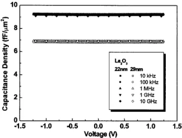
C-V characteristics at intermediate frequencies from 10 KHz to 1 MHz.—For precision analog circuit applications, MIM capacitors must be effective over a wide range of frequencies. Figure 2 plots the capacitance density vs. voltage (C-V) characteristics of La2O3 MIM capacitors. At 1 MHz, high capacitance densities of 9.2 and 6.9F/cm2are measured for La2O3capacitors with physical thick-nesses of 22 and 29 nm, respectively. The corresponding k values are 23 for La2O3dielectrics. C-V data at over 1 MHz are derived from measured S parameters and equivalent circuit models, consid-ered in a later section.
The capacitance variation, voltage-dependent capacitance (⌬C/C), is important in precision circuit applications, so ⌬C/C is determined from the plotted C-V measurements. Figure 3a and b plot⌬C/C for La2O3MIM capacitors, with physical thicknesses of 22 and 29 nm, respectively. The⌬C/C data below 1 MHz are taken from the C-V plot in Fig. 2, while those above 1 MHz are taken zE-mail: [email protected]
Journal of The Electrochemical Society, 151共7兲 F162-F165 共2004兲 0013-4651/2004/151共7兲/F162/4/$7.00 © The Electrochemical Society, Inc. F162
) unless CC License in place (see abstract).
ecsdl.org/site/terms_use
address. Redistribution subject to ECS terms of use (see
140.113.38.11
from the measured S parameters shown below and from the authors’ previously derived equations.14 The asymmetry of the ⌬C/C is caused by the difference between the top Al and bottom Pt elec-trodes, as in the case of the asymmetry in the J-V characteristics, plotted in Fig. 1. Notably, although⌬C/C is high at 10 KHz, it falls dramatically to a value of⬃100 ppm as the frequency is increased to above 1 GHz. Notably, the⌬C/C results are better than were obtained for AlTaOx,15and important for analog circuit matching.
Figure 4 plots⌬C/C and quadratic voltage coefficient, ␣, against frequency to elucidate further the frequency dependence of⌬C/C and related␣. The relationship between ␣ and ⌬C/C is expressed as follows
⌬C/C ⫽ ␣V2⫹ V 关1兴
The term is the linear voltage coefficient, and is less important than␣ according to the circuit cancellation method.20Again,⌬C/C and ␣ fall monotonically as the frequency is increased. Small ⌬C/C ⭐ 100 ppm and ␣ ⭐ 130 ppm/V2 are obtained as the fre-quency is increased into the gigahertz regime, implying that the high-k MIM capacitors can be used in precision circuits at operating frequencies into the gigahertz regime. High-k HfO2MIM capacitors
also exhibit declining ⌬C/C and ␣ as the frequency rises to 1 MHz;20a possible mechanism for this frequency dependence is the change in the relaxation time in the high-k dielectric, since the car-riers inside the high-k dielectric cannot follow the switching signal at very high signal frequencies.20This model also explains the con-tinuous decrease in⌬C/C and ␣ as the frequency increases into the gigahertz regime. Notably, the current rf circuits presently used in wireless communication are in the gigahertz regime共0.9–1.9 GHz for handset, 2.4 GHz for Bluetooth, 5.2–5.7 GHz for wireless LAN, and 3.1–10.6 GHz for ultrawide band兲. Hence, ⌬C/C in the giga-hertz regime is extremely important in both current and future rf communication.
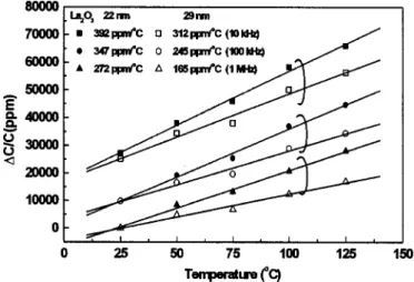
Weak dependence of capacitance on temperature is also an im-portant factor in circuit application. Figure 5 plots the ⌬C/C of La2O3 MIM capacitors as functions of temperature. The temperature-dependent⌬C/C declines as frequency increases, in a Figure 1. J-V characteristics of MIM capacitors with 22 and 29 nm La2O3
dielectrics. Asymmetry of J-V and breakdown voltage are related to the large difference between the work functions of Pt and Al.
Figure 2. C-V characteristics of MIM capacitors with 22 and 29 nm La2O3
dielectrics at various frequencies.
Figure 3. ⌬C/C of 共a兲 22 and 共b兲 29 nm La2O3 MIM capacitors as
func-tions of applied voltage at various frequencies.
Journal of The Electrochemical Society, 151共7兲 F162-F165 共2004兲 F163
) unless CC License in place (see abstract).
ecsdl.org/site/terms_use
address. Redistribution subject to ECS terms of use (see
140.113.38.11
manner consistent with Fig. 3. The⌬C/C increases with tempera-ture, exhibiting the same trend as other dielectric capacitors pub-lished in the literature.7
S-parameters and rf analysis from 200 MHz to 20 GHz.—The maximum frequency at which conventional C-V measurements can be made using a precision LCR meter is only 1 MHz; the capaci-tance C and⌬C/C at rf frequency must be extracted from measured S parameters. Figure 6a and b plot the measured S parameters of 22 and 29 nm La2O3MIM capacitors, respectively. Figure 7 shows the equivalent circuit model for MIM capacitors. Figure 2 and 3 also present extracted C and derived⌬C/C using our previously pub-lished equations and measured S parameters at 1 and 10 GHz. The ⌬C/C decreases monotonically by orders of magnitude as the fre-quency is increased into the gigahertz frefre-quency regime and is suf-ficiently low to support high-precision circuit applications20in this frequency regime.
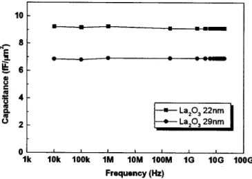
Figure 8 plots the La2O3 MIM capacitance densities vs. fre-quency. The intermediate frequency data are obtained directly from C-V measurements. The capacitance values at rf frequencies are extracted from the well-matched measured and modeled S param-eters in Fig. 6a and b. La2O3MIM capacitors exhibit a small drop in capacitance as the frequency is varied from 10 KHz to 20 GHz, indicating the excellence of high-k dielectrics formed at the low temperature of 400°C.
Figure 9 plots the dependence of the Q factor on frequency for high-k La2O3 MIM capacitors, whose parasitic inductance was de-Figure 4.⌬C/C and ␣ of La2O3and AlTaOxMIM capacitors as functions of frequency.
Figure 5.⌬C/C of La2O3MIM capacitors as a function of temperature.
Figure 6. Measured and simulated S parameters of共a兲 22 and 共b兲 29 nm
La2O3MIM capacitors.
Figure 7. Equivalent circuit model used to simulate MIM capacitor in the rf
regime.
Journal of The Electrochemical Society, 151共7兲 F162-F165 共2004兲 F164
) unless CC License in place (see abstract).
ecsdl.org/site/terms_use
address. Redistribution subject to ECS terms of use (see
140.113.38.11
embedded in the through transmission line. The de-embedded Q factor is high,⭓90, up to a resonant frequency of ⬃10 to 12 GHz. The Q factor decreases as the thickness of the dielectric falls be-cause the resistor loss parallel to the capacitor body falls, due to the larger leakage current, as indicated by the J-V characteristics.
Conclusions
High-k La2O3 dielectrics were processed at 400°C to achieve a high capacitance density of 9.2 fF/m2 and a low ⌬C/C ⭐ 100 ppm at 1 GHz. A high capacitance per unity area can be maintained from 10 KHz to 20 GHz, with a large Q factor⭓90. The good rf
device integrity of high-density La2O3 dielectric MIM capacitors can greatly reduce the chip size of rf circuits and is useful in preci-sion circuits at high frequencies.
Acknowledgments
The authors thank the National Science Council of the Republic of China, Taiwan, for financially supporting this research under con-tract no. NSC 92-2215-E-009-031. Dr. G. W. Huang at the National Nano Device Laboratory of Taiwan is appreciated for helping with the rf measurement.
National Chiao Tung University assisted in meeting the publication costs of this article.
References
1. C. H. Huang, C. H. Lai, J. C. Hsieh, J. Liu, and A. Chin, IEEE Microwave Wireless Comp. Lett., 12, 464共2002兲.
2. C. H. Huang, K. T. Chan, C. Y. Chen, A. Chin, G. W. Huang, C. Tseng, V. Liang, J. K. Chen, and S. C. Chien, IEEE RF-IC Int. Microwave Symp. Dig., 2003, 373. 3. Y. H. Wu, A. Chin, C. S. Liang, and C. C. Wu, IEEE RF-IC Int. Microwave Symp.
Dig., 2000, 151.
4. J. W. Lee, H. S. Song, K. M. Kim, J. M. Lee, and J. S. Roh, J. Electrochem. Soc., 149, F56共2002兲.
5. S. Y. Kang, H. J. Lim, C. S. Hwang, and H. J. Kim, J. Electrochem. Soc., 149, C317共2002兲.
6. C. P. Yue and S. S. Wong, IEEE MTT-S Int. Microwave Symp. Dig., 1999, 1625. 7. J. A. Babcock, S. G. Balster, A. Pinto, C. Dirnecker, P. Steinmann, R. Jumpertz, and
B. El-Kareh, IEEE Electron Device Lett., 22, 230共2001兲.
8. C.-M. Hung, Y. C. Ho, I. C. Wu, and K. O. , IEEE MTT-S Int. Microwave Symp. Dig., 1998, 505.
9. Z. Chen, L. Guo, M. Yu, and Y. Zhang, IEEE Microwave Wireless Comp. Lett., 12, 246共2002兲.
10. J. H. Lee, D. H. Kim, Y. S. Park, M. K. Sohn, and K. S. Seo, IEEE Microw. Guid. Wave Lett., 9, 345共1999兲.
11. K. Shao, S. Chu, K. W. Chew, G. P. Wu, C. H. Ng, N. Tan, B. Shen, A. Yin, and Z. Y. Zheng, in Proceedings of 6th International Conference on Solid-State and Integrated-Circuit Technology Digest, 2001, 243.
12. H. Iwai, S. Ohmi, S. Akama, C. Ohshima, A. Kikuchi, I. Kashiwagi, J. Taguchi, H. Yamamoto, J. Tonotani, Y. Kim, I. Ueda, A. Kuriyama, and Y. Yoshihara, Tech. Dig. - Int. Electron Devices Meet., 2002, 625.
13. S. J. Lee, H. F. Luan, C. H. Lee, T. S. Jeon, W. P. Bai, Y. Senzaki, D. Roberts, and D. L. Kwong, in Proceedings of Symposium on VLSI Technology, 2001, 133. 14. A. Chin, Y. H. Wu, S. B. Chen, C. C. Liao, and W. J. Chen, in Digest of Symposium
on VLSI Technology, 2000, 19.
15. M. Y. Yang, C. H. Huang, A. Chin, C. Zhu, M. F. Li, and D. L. Kwong, IEEE Electron Device Lett., 24, 306共2003兲.
16. S. B. Chen, J. H. Chou, A. Chin, J. C. Hsieh, and J. Liu, IEEE Electron Device Lett., 23, 185共2002兲.
17. H. Hu, C. Zhu, Y. F. Lu, M. F. Li, B. J. Cho, and W. K. Choi, IEEE Electron Device Lett., 23, 514共2002兲.
18. S. B. Chen, J. H. Chou, A. Chin, J. C. Hsieh, and J. Liu, IEEE MTT-S Int. Micro-wave Symp. Dig., 2002, 201.
19. C. H. Huang, M. Y. Yang, A. Chin, C. X. Zhu, M. F. Li, and D. L. Kwong, IEEE MTT-S Int. Microwave Symp. Dig., 2003, 507.
20. C. Zhu, H. Hu, X. Yu, A. Chin, M. F. Li, and D. L. Kwong, Tech. Dig. - Int. Electron Devices Meet., 2003, 879.
21. K. T. Chan, A. Chin, C. M. Kwei, D. T. Shien, and W. J. Lin, IEEE MTT-S Int. Microwave Symp. Dig., 2001, 763.
22. K. T. Chan, A. Chin, Y. B. Chen, Y.-D. Lin, D. T. S. Duh, and W. J. Lin, Tech. Dig. - Int. Electron Devices Meet., 2001, 903.
23. Y. H. Wu, A. Chin, K. H. Shih, C. C. Wu, C. P. Liao, S. C. Pai, and C. C. Chi, IEEE MTT-S Int. Microwave Symp. Dig., 2000, 221.
24. T. Park, H. J. Cho, J. D. Choe, S. Y. Han, S.-M. Jung, J. H. Jeong, B. Y. Nam, O. I. Kwon, J. N. Han, H. S. Kang, M. C. Chae, G. S. Yeo, S. W. Lee, D. Y. Lee, D. Park, K. Kim, E. Yoon, and J. H. Lee, Tech. Dig. - Int. Electron Devices Meet., 2003, 27.
Figure 8. Frequency-dependent capacitance of La2O3MIM capacitors with
two dielectric thicknesses.
Figure 9. Quality factor of La2O3 MIM capacitors as a function of
fre-quency.
Journal of The Electrochemical Society, 151共7兲 F162-F165 共2004兲 F165
) unless CC License in place (see abstract).
ecsdl.org/site/terms_use
address. Redistribution subject to ECS terms of use (see
140.113.38.11