IEEE ELECTRON DEVICE LETTERS, VOL. 32, NO. 10, OCTOBER 2011 1397
Ambient Stability Enhancement of Thin-Film
Transistor With InGaZnO Capped With
InGaZnO:N Bilayer Stack Channel Layers
Po-Tsun Liu, Senior Member, IEEE, Yi-Teh Chou, Li-Feng Teng, Fu-Hai Li,
Chur-Shyang Fuh, and Han-Ping D. Shieh, Fellow, IEEE
Abstract—A thin-film transistor (TFT) with bilayer stack
struc-ture of amorphous nitrogenated InGaZnO (IGZO) (a-IGZO:N) on an IGZO channel is proposed to enhance device stability. The a-IGZO:N acting as a back-channel passivation (BCP) is formed sequentially just after the sputter-deposited amorphous IGZO (a-IGZO) film with in situ nitrogen incorporation process. The a-IGZO:N can effectively prevent the a-IGZO channel from ex-posing to the atmosphere and retarding interactions with ambient oxygen species. Also, the optical energy bandgap of the a-IGZO:N film is decreased due to the addition of nitrogen. This causes the a-IGZO TFT with a-IGZO:N BCP to exhibit high immunity to the ultraviolet-radiation impact.
Index Terms—InGaZnO (IGZO), in situ back-channel
passiva-tion (BCP), nitrogenated InGaZnO (IGZO:N).
I. INTRODUCTION
T
RANSPARENT amorphous indium (In) gallium (Ga) zinc (Zn) oxide is one of the most glaring candidates acting as semiconductor channel layer in thin-film transistor (TFT) technology for matrix liquid crystal displays and active-matrix organic light-emitting diode displays [1], [2]. There are some critical issues of electrical stability present in the amorphous InGaZnO (IGZO) (a-IGZO) TFT for the easy ab-sorption and deab-sorption reactions of the oxygen atom from the surrounding atmosphere [3], [4]. Various back-channel passivation (BCP) methods have been proposed to isolate the a-IGZO channel from the atmosphere [5], [6], but they were not successive process in the same reaction chamber as the a-IGZO sputter deposition. It will thereby increase the possibil-ity of the a-IGZO layer exposing to the atmosphere during the transportation process from the finished a-IGZO to BCP film formation. The affinity of BCPs with the a-IGZO channel alsoManuscript received June 14, 2011; accepted July 22, 2011. Date of publi-cation August 21, 2011; date of current version September 28, 2011. This work was supported by the National Science Council under Contract NSC 100-2628-E-009-016 -MY3. The review of this letter was arranged by Editor A. Nathan.
P.-T. Liu and H.-P. D. Shieh are with the Department of Photonics and the Display Institute, National Chiao Tung University, Hsinchu 30010, Taiwan (e-mail: [email protected]).
Y.-T. Chou, L.-F. Teng, and F.-H. Li are with the Department of Photonics and the Institute of Electro-Optical Engineering, National Chiao Tung Univer-sity, Hsinchu 30010, Taiwan.
C.-S. Fuh is with the Department of Electronics Engineering and the Institute of Electronics, National Chiao Tung University, Hsinchu 30010, Taiwan.
Color versions of one or more of the figures in this letter are available online at http://ieeexplore.ieee.org.
Digital Object Identifier 10.1109/LED.2011.2163181
had the impact on electrical characteristics of a-IGZO TFTs [7]. In addition to the environment-dependent metastability, the a-IGZO film with an energy bandgap of 3.5–3.8 eV is sensitive to ultraviolet (UV) radiation [8], [9]. The exposure to UV radia-tion usually occurs in the photolithography process during TFT array manufacture, module encapsulation, and even the TFT-based circuit operation under the atmosphere. The UV radiation can cause a disturbance of oxygen atoms in the a-IGZO film and result in the threshold voltage (Vth) shift toward the relatively negative voltage [10], [11]. The UV-shielding effects of the BCP layers on the a-IGZO TFT were little studied. In this letter, we propose an a-IGZO TFT device with in situ BCP of amorphous nitrogenated IGZO (a-IGZO:N) for stabilizing the device characteristics. The effects of the a-IGZO:N layer on both the ambient stability and the immunity to UV-radiation impact are also investigated comprehensively by electrical and optical analysis methods.
II. EXPERIMENT
An inverted staggered TFT structure is studied in this letter. A 100-nm-thick thermal oxide was first grown on an n+heavily doped silicon substrate in a thermal furnace at 650 ◦C. The low-resistivity substrate also acted as the gate electrode of the blanket samples. The 50-nm-thick a-IGZO active channel layer was then formed by dc sputtering with a power of 100 W and an argon (Ar) gas flow rate of 10 sccm at room temperature. After finishing the a-IGZO film, N2 gas with a flow rate of 2 sccm was in situ injected to the deposition chamber without breaking a vacuum to form the a-IGZO:N layer. The thickness of the a-IGZO:N film was 10 nm. The deposition pressure was also fixed at 5× 10⁻³ torr. The In:Ga:Zn:O:N atomic ratio of the a-IGZO:N film deposited with the N2 flow of 2 sccm was 1:1:0.8:5.2:1.8, while that of the a-IGZO film without the nitrogen incorporation was 1:1:0.7:5.4:0, respectively, by Rutherford backscattering spectrometry analysis. In our previ-ous study, the analysis on chemical compositions has indicated that the nitrogen species in the a-IGZO:N thin film has an electronic state similar to the one in Zn3N2-based material [12]. The active island was defined through a shadow mask process, and then, a 50-nm-thick indium tin oxide layer was formed subsequently as source/drain electrodes. Finally, all specimens were thermally annealed in a thermal furnace at 350◦C for 1.5 h. The 100-nm-thick a-IGZO:N films prepared with different N2 gas flow rates, ranging from 0 to 2 sccm,
1398 IEEE ELECTRON DEVICE LETTERS, VOL. 32, NO. 10, OCTOBER 2011
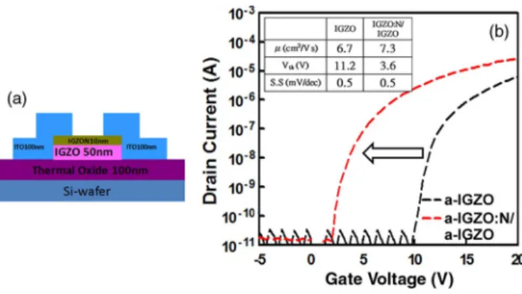
Fig. 1. (a) Schematic TFT device structure with a-IGZO:N/a-IGZO stacked channel layers, where the a-IGZO:N acts as a capping layer on the a-IGZO channel. (b) Transfer characteristics of a-IGZO TFT devices with and without the a-IGZO:N channel passivation layer. The a-IGZO:N film was sputter deposited at N2 flow rate of 2 sccm. The inset shows several key device
parameters, including threshold voltage (Vth), subthreshold swing (S.S), and
carrier mobility (μ).
were also deposited on a Corning Eagle 2000 glass substrate for optical transmittance analysis.
III. RESULTS ANDDISCUSSIONS
The TFT device with the a-IGZO:N film acting as a capping layer on the a-IGZO channel is referred to as the a-IGZO:N/ a-IGZO TFT, schematically shown in Fig. 1(a). The transfer characteristics of the a-IGZO:N/a-IGZO TFT in comparison with the a-IGZO TFT without the a-IGZO:N passivation layer are shown in Fig. 1(b). The corresponding device parameters were extracted and shown in the inset in Fig. 1(b). Both the increase of the carrier mobility and the decrease of Vthvalues are clearly observed in the a-IGZO:N/a-IGZO TFT device. The difference in the electronegativity between oxygen and nitrogen could be another possible cause for the Vth shift, in addition to a-IGZO:N effectively blocking the absorption of ambient oxygen to the a-IGZO channel [12]. The electronegativities of oxygen and nitrogen are 3.44 and 3.04, respectively, and they specifically describe the ability of an atom to attract a shared electron to itself [13]. The effective carrier concentration in a conductive oxide semiconductor might be increased due to the doping of nitrogen with low electronegativity. In this work, the slight incorporation of nitrogen into the a-IGZO channel could occur during the sequent film deposition of a-IGZO/a-IGZO:N stack layers. Therefore, the a-IGZO/a-IGZO:N TFT can exhibit lower Vththan the a-IGZO TFT.
Furthermore, the time-dependent Vth values of the a-IGZO TFT and a-IGZO:N/a-IGZO TFT devices under the atmosphere with 50% relative humidity at 25◦C for 7 days are shown in Fig. 2(a). It is first observed that Vthdecreases with increasing the storage time under the atmosphere. The electrical instability of IGZO-based materials is strongly related to the inactive oxygen in the a-IGZO channel layer. For the inactive oxygen, the oxygen desorption reaction easily occurs continuously in the passivation-free back-channel region and forms oxygen va-cancies in the a-IGZO film [6], resultantly causing the reduction of Vthvalues with prolonged staying durations. The average of
Vthshifts during the entire measurement period is−4.57 V for
Fig. 2. (a) Variation of Vthvalues for a-IGZO TFT devices with and without
a-IGZO:N capping layer staying under the ambient atmosphere with 50% relative humidity at 25◦C for 7 days. Each error bar includes five different measuring results for each TFT device. (b) Threshold voltage shifts of gate bias stress a-IGZO TFT devices without and with a-IGZO:N channel capping layers (10, 50, and 100 nm). The conditions of gate bias stress test are under the positive and negative gate biases with electrical field of 1 MV/cm, respectively, for 104s.
the a-IGZO TFT, while it reduces to−2.09 V for the a-IGZO:N/ a-IGZO TFT device. In addition to the decrease of the Vthshift, the shrinkage of the measuring error bars also indicates that electrical uniformity of the a-IGZO:N/a-IGZO TFT device is significantly improved in comparison with that of the a-IGZO TFT. When the nitrogen is in situ doped into the a-IGZO to form the a-IGZO:N film, nitrogen atoms can partially replace the inactive oxygen atoms and reduce the oxygen desorption reaction occurring in the a-IGZO:N film. The a-IGZO:N pas-sivation layer also can diminish the desorption of oxygen out of the underneath a-IGZO channel layer. The variation of Vth values with increasing the storage duration is thereby decreased for the a-IGZO:N/a-IGZO TFT device. To verify the effects of the a-IGZO:N layer on electrical reliability enhancement, the gate bias stress testing with an electrical field of 1 MV/cm for 104s at room temperature was applied to a-IGZO TFT devices with and without the a-IGZO:N BCP layer. Fig. 2(b) shows Vth shifts of the a-IGZO TFT with different thicknesses (10, 50, and 100 nm) of capping a-IGZO:N after the positive/negative gate bias stress as a function of stress time durations. It is clearly observed that the Vthshifts of the a-IGZO:N/a-IGZO TFT after the positive or negative gate bias stress are all less than those of the a-IGZO TFT. The bias electrical field can influence the number of carrier concentrations accumulated in the a-IGZO channel region and disturb the oxygen absorption/desorption reaction between the back channel and ambient air [3], [4]. By using the in situ deposited a-IGZO:N channel passivation which is less sensitive to the ambient, oxygen and moisture species can be effectively prevented from contacting with the a-IGZO channel layer. Thus, electrical characteristics of the a-IGZO/ a-IGZO:N TFT device keep stable even after gate bias stress and exhibit less Vthshift.
Optical properties of the a-IGZO films with different con-centrations of nitrogen were studied, as shown in Fig. 3(a). The transparency of the a-IGZO:N films is high in the visible region, which is the same for the a-IGZO film, and it is in the range of 94% ± 1% at 550-nm measuring wavelength. In contrast, an even obvious optical absorption of the a-IGZO:N film is observed in the UV-light region in comparison with that of the a-IGZO film without nitrogen incorporation. The optical trans-parency of dielectric materials is proportional to their optical
LIU et al.: AMBIENT STABILITY ENHANCEMENT OF TFT WITH IGZO CAPPED WITH IGZO:N LAYERS 1399
Fig. 3. (a) Transmittance of a-IGZO:N films on a glass substrate. The a-IGZO:N films were sputter deposited with in situ N2gas flow rates ranging
from 0 to 2 sccm. The inset shows the corresponding values of optical energy bandgap (Eg) of a-IGZO:N films prepared with different N2 gas flow rates.
(b) Threshold voltage shifts of a-IGZO TFT devices with and without a-IGZO:N capping layer under light illumination with wavelengths ranging from 250 to 600 nm. The thickness of a-IGZO:N capping layers includes 10, 50, and 100 nm.
bandgaps (Eg), which can be theoretically obtained according
to Tauc’s model [14]. The obtained values of optical bandgaps for the a-IGZO films deposited with different N2gas flow rates are summarized in the inset table in Fig. 3(a). The optical bandgaps of the a-IGZO:N films decrease from 3.6 down to 3.2 eV with the increase of N2 gas flow rate up to 2 sccm during a-IGZO film deposition. The UV absorption coefficient of the IGZO:N film is higher than that of the IGZO film, and the coefficients are 1.08× 10⁴ and 7.41× 103 cm−1 for the IGZO:N and IGZO, respectively, under g-line UV illumination. It also exhibits a great potential for the a-IGZO:N film to absorb UV light and prevent the a-IGZO active channel from UV-radiation impact. Fig. 3(b) shows the Vth shifts of the a-IGZO TFT devices with different thicknesses of a-IGZO:N capping layers under the light radiation with wavelengths ranging from 600 to 300 nm. The Vth value keeps intact for the visible-light illumination with wavelengths between 600 and 400 nm, while obvious Vthshifts are observed in the UV-light radiation regions with wavelengths shorter than around 350 nm. The UV wavelengths less than 436 nm are targeted to be blocked from degrading the channel layer and TFT device performance in this work. It can be particularly noted that the Vthshift of the TFT device under UV-light radiation is remarkably reduced with increasing the a-IGZO:N passivation layer thickness ranging from 10 to 100 nm. These aforementioned results confirm the effects of the a-IGZO:N channel passivation layer on the ambi-ent stability enhancemambi-ent for the IGZO-based TFT technology applications.
IV. CONCLUSION
The a-IGZO TFT with the in situ a-IGZO:N channel passi-vation layer has been proposed for enhancing device stability. Electrical reliability and uniformity of a-IGZO:N/a-IGZO TFT
were improved obviously under electric operation at the atmo-sphere, even after gate bias stress. The a-IGZO:N/a-IGZO TFT device also exhibited superior immunity against UV-radiation impact, since the top layer of the a-IGZO:N film played the role of UV-light shield layer for the underneath a-IGZO channel. The efficiency of UV shielding was promoted with increasing the thickness of the a-IGZO:N capping layer. Therefore, the a-IGZO:N/a-IGZO TFT structure can effectively enhance device reliability and stability to the ambient.
REFERENCES
[1] J. S. Park, K. S. Kim, Y. G. Park, and Y. G. Mo, “Novel ZrInZnO thin-film transistor with excellent stability,” Adv. Mater., vol. 21, no. 3, pp. 329– 333, Jan. 2009.
[2] S. Narushima, H. Mizoguchi, K. Shimizu, K. Ueda, H. Ohta, M. Hirano, T. Kamiya, and H. Hosono, “A p-type amorphous oxide semiconductor and room temperature fabrication of amorphous oxide p-n heterojunction diodes,” Adv. Mater., vol. 15, no. 17, pp. 1409–1413, Sep. 2003. [3] D. Kang, H. Lim, C. Kim, I. Song, J. Park, Y. Park, and J. G. Chung,
“Amorphous gallium indium zinc oxide thin film transistors: Sensitive to oxygen molecules,” Appl. Phys. Lett., vol. 90, no. 19, p. 192 101, May 2007.
[4] P. T. Liu, Y. T. Chou, and L. F. Teng, “Environment-dependent meta-stability of passivation-free indium zinc oxide thin film transistor after gate bias stress,” Appl. Phys. Lett., vol. 95, no. 23, p. 233 504, Dec. 2009. [5] D. Stryakhilev, J. S. Park, J. Lee, T. W. Kim, Y. S. Pyo, D. B. Lee, E. H. Kim, D. U. Jin, and Y. G. Mo, “Electrical Instability of a-In–Ga–Zn–O TFTs biased below accumulation threshold,”
Electro-chem. Solid-State Lett., vol. 12, no. 11, pp. J101–J104, 2009.
[6] K. Takechi, M. Nakata, K. Azuma, H. Yamaguchi, and S. Kaneko, “Dual-gate characteristics of amorphous thin-film transistors as compared to those of hydrogenated amorphous silicon thin-film transistors,” IEEE
Trans. Electron Devices, vol. 56, no. 9, pp. 2027–2033, Sep. 2009.
[7] S. E. Liu, M. J. Yu, C. Y. Lin, G. T. Ho, C. C. Cheng, C. M. Lai, C. J. Lin, Y. C. King, and Y. H. Yeh, “Influence of passivation layers on characteristics of a-InGaZnO thin-film transistors,” IEEE Electron Device
Lett., vol. 32, no. 2, pp. 161–163, Feb. 2011.
[8] D. K. Seo, B. H. Kong, and H. K. Cho, “Composition controlled super-lattice InGaO3(ZnO)m thin films by thickness of ZnO buffer layers and thermal treatment,” Cryst. Growth Des., vol. 10, no. 10, pp. 4638–4641, 2010.
[9] H. Hiramatsu, K. Ueda, H. Ohta, T. Kamiya, M. Hirano, and H. Hosonoe, “Excitonic blue luminescence from p-LaCuOSe/n-InGaZn5O8light-emitting diode at room temperature,” Appl. Phys. Lett.,
vol. 87, no. 21, p. 211 107, Nov. 2005.
[10] K. Takechi, M. Nakata, T. Eguchi, H. Yamaguchi, and S. Kaneko, “Com-parison of ultraviolet photo-field effects between hydrogenated amor-phous silicon and amoramor-phous InGaZnO4 thin-film transistors,” Jpn. J.
Appl. Phys., vol. 48, no. 1, p. 010 203, Jan. 2009.
[11] P. T. Liu, Y. T. Chou, and L. F. Teng, “Charge pumping method for photosensor application by using amorphous indium–zinc oxide thin film transistors,” Appl. Phys. Lett., vol. 94, no. 24, p. 242 101, Jun. 2009. [12] P. T. Liu, Y. T. Chou, L. F. Teng, F. H. Li, and H. P. Shieh, “Nitrogenated
amorphous InGaZnO thin film transistor,” Appl. Phys. Lett., vol. 98, no. 5, p. 052 102, Jan. 2011.
[13] S. S. Zumdahl, Chemical Principles, 6th ed. Boston, MA: Houghton Mifflin, 2007.
[14] D. L. Wood and J. Tauc, “Weak absorption tails in amorphous semicon-ductors,” Phys. Rev. B, Condens. Matter, vol. 5, no. 8, pp. 3144–3151, Apr. 1972.
[15] S. Y. Sung, J. H. Choi, U. B. Han, K. C. Lee, J. H. Lee, J. J. Kim, W. Lim, S. J. Pearton, D. P. Norton, and Y. W. Heo, “Effects of ambient atmosphere on the transfer characteristics and gate-bias stress stability of amorphous indium–gallium–zinc oxide thin-film transistors,” Appl. Phys.