i
國
立
交
通
大
學
材料科學與工程學系
博
士
論
文
(鎳、鈦與鎢)氧化物之電性及應用於電阻式隨機
記憶體研究
Electric Characteristics and Application of (Nickel, Titanium and
Tungsten) Oxides on Resistive Random Access Memory
(RRAM)
研 究 生:李明道
指導教授:姚永德 教授
ii
(鎳、鈦與鎢)氧化物之電性及應用於電阻式隨機記憶體研究
Electric Characteristics and Application of (Nickel, Titanium and
Tungsten) Oxides on Resistive Random Access Memory
(RRAM)
研 究 生:李明道 Student : Ming-Daou Lee
指導教授:姚永德 Advisor : Yeong-Der Yao
國 立 交 通 大 學
材料科學與工程學系
博 士 論 文
A Thesis
Submitted to Department of Materials Science and Engineering National Chiao Tung University
in partial Fulfillment of the Requirements for the Degree of Doctor of Philosophy
in
Materials Science and Engineering January 2012
Hsinchu, Taiwan, Republic of China
i (鎳、鈦與鎢)氧化物之電性及應用於電阻式隨機記憶體研究 學生:李明道 指導教授: 姚永德教授 國立交通大學 材料科學與工程 學系﹙研究所﹚博士班 摘 要 近年來,由於傳統浮動閘極結構之非揮發性記憶體(Flash memory)在小於二十 奈米節點技術將面臨其物理極限,一些新式非揮發性記憶體如磁阻式記憶體 (MRAM)、相變化記憶體(PCRAM)、以及電阻式記憶體(RRAM)之研究在下世代資 訊儲存應用也變得越趨重要。另一方面,由於某些電阻式記憶體材料具備 CMOS 製程完全相容、高存取速度、高可靠度、以及高容量等優越特性在下世代記憶體 元件中具有高商業價值潛力,故本篇論文也聚焦於 RRAM 之相關研究。 雖然有很多金屬氧化物材料可應用於 RRAM 元件,然而與 CMOS 製程完全相 容的材料包含氧化鎳、氧化鈦以及氧化鎢三種材料而且在 RRAM 特性上也有不錯 的表現。在 CMOS 製程中鎳化矽(NiSi)用於中段製程,其作用為降低金氧半導體 (MOS)接面上的阻值,氮化鈦(TiN)則用於中段以及後段製程(BEOL),其目的為增 加金屬附著性以及當作擴散阻障層,而金屬鎢(W)則廣用於中段接觸(Contact)製 程,為 CMOS 元件與後段電路連接的主要金屬材料,綜觀以上特點,以氧化鎳、 氧化鈦或是氧化鎢作為電阻式記憶體元件材料可與現今半導體 CMOS 製程完全相 容。而在本篇論文中將深入探討這三種材料之 RRAM 特性包括電性表現、電阻翻 轉機制以及相關之應用。 在實驗中我們發現氧化鎳材料屬於多晶結構而且具有雙極式 (Bipolar) RRAM 特性,其電性顯示出薄膜特性而且電性表現與氧化程度有著直接的關係,氧化程 度越高的樣品其電阻變化也相對明顯,而電子的傳導遵循著蕭基發射(Schottky emission)傳導機制,藉由此一機制可以得知蕭基能障的變化與元件電阻的變化息息 相關,此外更可以得知氧化程度越低的樣品其介電常數越高,這也進一步解釋了 低氧化程度的樣品在電阻翻轉過程中需要更大的外加電壓才足夠抵銷樣品內部所 產生的反向電場。 類似於氧化鎳材料系統,氧化鈦材料同樣擁有雙極式 RRAM 特性,其電性表 現顯示出明顯的界面特性,薄膜厚度對其電性表現影響不大,其電子的傳導機制 與氧化鎳材料相同都遵循著蕭基發射傳導機制,而且蕭基能障的變化也與元件電 阻的變化有著直接的關係,而在氧化鈦/氧化矽複合材料的實驗當中進一步證實氧 化鈦 RRAM 的界面特性,而且此一複合材料的資訊保存能力也比單一氧化鈦薄膜 有著明顯的改善。 而在氧化鎢薄膜的實驗當中,我們發現這種材料有著多方面應用的潛力,舉 例來說,它不但可以用於單次儲存(OTP)而且可以用於多次儲存(MTP)記憶體裝
ii 置,而在多次儲存記憶體裝置中又可以使用雙極式以及單極式(Unipolar)操作來控 制其電阻阻態,而且耐久性皆大於一千次,由於這種材料也具有相當大的電阻阻 距,因此非常適合用於多層單元(MLC)儲存記憶體的應用,而且在製程微縮的實驗 中得知氧化鎢電阻式記憶體有著製程微縮的可行性,這種材料也展現出高可靠度 特性,例如在攝氏二百五十度的高溫環境之下表現出超過一千小時的熱穩定性。 而在電子傳導機制中氧化鎢電阻式記憶體之低電阻狀態表現出接近於導體的 minimum-metallic-conductivity (MMC) 傳 導 機 制 , 而 高 電 阻 狀 態 則 遵 循 著 variable-range-hopping (VRH) 傳導機制,而且根據計算可以得到高電阻狀態之躍遷 距離大約為十五 Å 。 綜觀以上三種材料的電性表現,氧化鎳以及氧化鈦材料由於界面之電荷效應 的影響在電子特性上並沒有比較傑出的表現,然而由於塊材特性的氧化鎢材料擁 有包括單次儲存(OTP)、多次儲存(MTP)、多層單元(MLC)儲存記憶體應用、雙極 式操作以及單極式操作等優越特性,在 RRAM 領域有著較高的商業應用潛力。
iii
Electric Characteristics and Application of (Nickel, Titanium and Tungsten) Oxides on Resistive Random Access Memory (RRAM)
Student : Ming-Daou Lee Advisor : Yeong-Der Yao
Department of Materials Science and Engineering National Chiao Tung University
ABSTRACT
Due to the fact that traditional nonvolatile memory (Flash memory) with polycrystalline floating-gate structure will face the physical limitation below 20nm technology node, some emerging non-volatile memories such as magnetic random access memory (MRAM), phase change random access memory (PCRAM), and resistive random access memory (RRAM) are widely investigated. Since the advantages of RRAM include CMOS fully compatibility, high speed operation, good reliability, and high capacity, RRAM exhibits high potential in commercial applications for the next generation. The RRAM study is thus the main theme of this thesis.
Although there are several materials successfully revealing resistance bistability under a certain electrical operation, it’s a pity that their CMOS compatibility is limited. Recently, metallic oxides by nickel (Ni), titanium (Ti), and tungsten (W) are reported to present good RRAM performance. Meanwhile, in the CMOS integration, nickel silicide (NiSi) is used in the middle-end-of-line (MEOL) process for reducing the contact resistance of both N- and P-MOS. Titanium nitride (TiN) is utilized respectively for back-end-of-line (BEOL) and MEOL processes to increase the metal adhesion and diffusion barrier capability. Tungsten (W) is widely accepted in the contact plug fabrication and it is the main material for the interconnection between CMOS device and BEOL circuit. Accordingly, RRAM materials with nickel oxide (NiOx), titanium oxide (TiOx), and tungsten oxide (WOx) are also the CMOS fully compatible materials. In this thesis, we discuss the RRAM characteristics of all these three materials in details, including the electrical performance, the switching model, and the applications.
In NiOx-based RRAM study, bipolar resistance switching behavior in polycrystalline thin film shows obvious thin film contribution and oxygen content effects on on/off ratio; that is, the higher oxygen content sample exhibits higher on/off ratio. Also, its conduction mechanism entirely follows the Schottky emission, and the on/off ratio is strongly barrier height dependent. According to Schottky emission simulation, NiOx-based RRAM thin film with low oxygen content presents higher
iv
dielectric constant. The result could explain why NiOx-based RRAM thin film with low oxygen content needs higher energy to countervail the inner opposite electric field in the resistive switching process.
In TiOx-based RRAM study, similar to the previous NiOx-based system, TiOx-based RRAM also shows bipolar resistance switching behavior. It is clear that the interfacial characteristics between TiOx-based thin film and electrode dominates the electrical performance, while the thickness effect of TiOx thin film on resistance switching properties is relatively minor. Again, similar to NiOx-based system, the transportation follows the Schottky emission and the on/off ratio is found to be strongly barrier height dependent. In addition, the designed experiment, TiOx / SiO2 hybrid system, indicates the importance of interfacial contribution, and the data retention is further found to be improved by this hybrid system.
In WOx-based RRAM study, we found this system has high potential for several applications, such as the memory device with one-time-programming (OTP) and multi-times-programming (MTP) functionality. For MTP application, resistive state of WOx-based system can be switched reversibly by either bipolar or unipolar operation with the cycle endurance of exceeding 1000. On the other hand, this RRAM system is suitable for the multi-level-cell (MLC) application, too, due to its sufficient on/off ratio higher than 1000X. The highly scalable ability of this system is also discussed in this thesis. Meanwhile, a reliable characteristics is also demonstrated: high thermal stability of over 1000 hours at 250℃.
With the mathematical fitting of WOx-based RRAM system, the electron conduction of high resistance state and low resistance state respectively follow the variable-range-hopping (VRH) transportation and minimum-metallic-conductivity (MMC). According to the fitting results, the hopping distance of high resistance state is found to be around 15Å .
NiOx, TiOx, and WOx materials, which are all CMOS fully compatible without contamination risk, are summarized here for RRAM applications. For the overall comparison of RRAM functionality, interfacial contribution (NiOx or TiOx) cannot provide better characteristics than bulk contribution (WOx) because the electron charging affects at interface to worsen the electrical performance of such kind of RRAM system. And the system with bulk contribution in turn could provide high potential for several commercial applications on electron devices, such as OPT, MTP, MLC, and unipolar operation as well.
v
誌
謝
首先要感謝指導老師姚永德教授這些年來的栽培,讓學生學習到很多做人以 及做事的方法,在學期間不管是學業或者生活方面老師總是能夠適時給予指導以 及幫助,在學業方面老師讓學生在面對問題的時候能夠正面思考以解決問題,而 在待人處事方面老師更是學生的榜樣,凡事嚴以律己寬以待人,讓學生了解待人 圓融的重要。 再來要感謝盧志權老師在工研院時的教導,讓學生在就學期間可以接觸許多 製程以及分析儀器,從廠商的聯繫到機台的組裝都能夠讓學生親自參與,在這段 期間讓學生學到相當多的專業技能,從軟體的機台設計到硬體的儀器組裝學生都 有參與,而這些技能也在學生之後的就業上也幫了很大的忙。 之後要感謝何家驊博士的指導與提攜,讓學生瞭解半導體界的相關知識,不 管是邏輯或是記憶體方面都讓學生受益良多,而在就業方面何博也讓學生明白人 和的重要性,凡事以和為貴這樣公司所交代的事才能進行的順利,而在帶人方面 也要善待下屬才能夠完全發揮團隊合作的功能。 這裡也要感謝劉瑞琛協理、謝光宇處長以及楊富量主任的栽培,感謝瀛文、 藍青、泰彥跟維志在工研院時期的幫忙,也感謝所有共事過的同事夥伴,在這一 路上的照顧以及扶持。 最後要感謝老婆育芬這些年默默付出的辛勞,為這個家盡心盡力讓我在工作 以及學業上無後顧之憂。
vi 目 錄 中文摘要 ……… i 英文摘要 ……… iii 誌謝 ……… v 目錄 ……… vi 表目錄 ……… viii 圖目錄 ……… ix 一、 Introduction……… 1
1.1 Floating gate Flash……… 3
1.1.1 NOR Flash……… 4
1.1.2 NAND Flash……… 5
1.2 Magnetic Random Access Memory (MRAM)……… 6
1.3 Phase Change Random Access Memory (PCRAM)……… 7
1.4 Resistance Random Access Memory (RRAM)……… 9
1.4.1 The history of RRAM development……… 10
1.4.2 Metal-Oxide RRAM……… 13
二、 Experiment……… 14
2.1 BEOL Process flow……… 14
2.1.1 Deposition……… 15
2.1.2 Lithography……… 17
2.1.3 Etching……… 18
2.1.4 Chemical Mechanical Polishing (CMP)……… 19
2.2 Layout……… 20
2.3 Analysis……… 21
2.3.1.1 Cycle Endurance Measurement………… 22
2.3.1.2 Thermal Stability Measurement………… 22
2.3.1.3 Stress Test………… 23
2.3.1.4 Data retention Measurement 24 2.3.2.1 XPS Analysis 25 2.3.2.2 TEM Analysis 26 2.3.2.3 PPMS Measurement 27 2.3.1 Electrical analysis……… 22 2.3.2 Material analysis……… 25 三、 Principle……… 28
3.1 Basic resistance switching characteristics and nomenclature………… 28
3.1.1 Bipolar, unipolar, nonpolar operation……… 30
3.1.2 Basic resistance switching nomenclature……… 32
3.2 Electron transportation mechanism ……… 33
3.2.1 The metallic transportation mechanism ……… 33
3.2.2 The Schottky emission ……… 34
3.2.3 The Poole-Frenkel emission ……… 35
3.2.4 The electron hopping transportation mechanism ……… 37
3.2.5 The space-charge-limited-current (SCLC) ……… 38
3.2.6 The trap-assisted-tunneling (TAT) ……… 40
3.3 Resistance switching mechanism ……… 42
3.3.1 The conducting filament characteristics ……… 42
vii
3.4 Resistance switching model ……… 45
3.4.1 The “Rupture Ball” model ……… 46
3.4.2 The stochastic model ……… 47
3.4.3 The thermal dissolution model ……… 48
3.4.4 The two-variable-resistor model ……… 51
3.4.5 The compact model ……… 52
3.4.6 The filament anodization model ……… 55
3.4.7 The numerical model ……… 55
3.5 The key physical parameters influence RRAM performance ………… 58
3.5.1 Thickness ……… 58
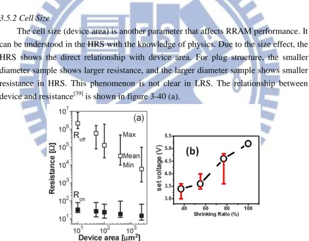
3.5.2 Cell size ……… 59
3.5.3 Electrode ……… 60
3.5.4 Doping effect ……… 61
3.5.5 Electric field ……… 61
3.5.6 Density of oxygen vacancy ……… 63
四、 Results……… 64
4.1 Outline of results……… 64
4.2 NiOx based RRAM……… 65
4.3 TiOx based RRAM……… 73
4.4 WOx based RRAM……… 79
4.4.1 One-time-programming (OTP) RRAM……… 82
4.4.2 Bipolar multi-times-programming (MTP) RRAM……… 87
4.4.3 Unipolar multi-times-programming (MTP) RRAM……… 93
4.4.4 Scaling effect……… 100
4.5 Metal-oxide RRAM organization ……… 103
五、 Summary……… 104
Reference……… 105
viii
表 目 錄
Table 1-1 Non-volatile memories comparison……… 1
ix
圖 目 錄
Figure 1-1 Floating gate structure Flash sketch ……… 3
Figure 1-2 Programmed and Erased states of Flash ……… 4
Figure 1-3 (a) The reading electrical character of Flash (b) The electrical symbol of Flash device ……… 4
Figure 1-4 NOR type Flash device circuit ……… 5
Figure 1-5 NOR Flash (a) write process by channel hot electron injection. (b) erase process by F/N tunneling ……… 5
Figure 1-6 NAND type Flash device circuit ……… 6
Figure 1-7 NAND Flash (a) write process (b) erase process by F/N tunneling ……… 6
Figure 1-8 The magneto resistance curve ……… 7
Figure 1-9 The MRAM structure sketch ……… 7
Figure 1-10 The sketch of PCRAM ……… 8
Figure 1-11 The working mechanism of PCRAM ……… 8
Figure 1-12 The sketch of RRAM ……… 9
Figure 1-13 The electrical character of bipolar method RRAM ……… 9
Figure 1-14 The electrical character of unipolar method RRAM ……… 10
Figure 1-15 The early electric characteristics in niobium oxide film……… 11
Figure 1-16 The cycle endurance data of CMR-based RRAM……… 11
Figure 1-17 The thermal stability test of unipolar operation tungsten oxide film… 12 Figure 1-18 The elements (red marked) that their metal-oxide were found to exhibit resistance switching characteristics by bipolar (solid line) and unipolar operation. The metal oxide with dash line can be switched by both bipolar and unipolar operation……… 13
Figure 2-1 The sketch of semiconductor process ……… 14
Figure 2-2 The BEOL process flow and the sketch of BEOL profile ……… 14
Figure 2-3 The sketch of physics vapor deposition (PVD) system ……… 15
Figure 2-4 The sketch of chemical vapor deposition (CVD) process ……… 16
Figure 2-5 The sketch of IBD system……… 17
Figure 2-6 The sketch of lithography process ……… 18
Figure 2-7 The anisotropic and isotropic etching process ……… 19
Figure 2-8 The sketch of dry etching process ……… 19
Figure 2-9 The sketch of chemical mechanical polishing (CMP) process ……… 20
Figure 2-10 The top-view and cross-section of nickel oxide and titanium oxide RRAM structure ……… 20
Figure 2-11 The top-view and cross-section of tungsten oxide RRAM structure 21
Figure 2-12 The 2 bits/cell cycle endurance test of RRAM……… 22
Figure 2-13 The typical thermal stability test ……… 23
Figure 2-14 The typical stress test of RRAM ……… 23
Figure 2-15 The data retention test of 2bits/cell RRAM device ……… 24
Figure 2-16 The typical read disturb test of RRAM device ……… 25
Figure 2-17 The sketch of X-ray photoelectron spectroscopy (XPS) ……… 26
Figure 2-18 The sketch of transmission electron microscopy (TEM) ……… 27
Figure 3-1 The typical dc sweep bipolar operation characteristics……… 29
Figure 3-2 The bipolar operation characteristics by applied pulse voltage……… 30
Figure 3-3 The typical unipolar and nonpolar operation characteristics………… 31
x
Figure 3-5 The resistance switching characteristics of unipolar RRAM………… 32
Figure 3-6 The multiple-level-cell (MLC) of 2bits/cell RRAM……… 33
Figure 3-7 The temperature dependence relationship of metal electrical characteristics……… 34
Figure 3-8 The energy band diagram of a metal-semiconductor contact………… 34
Figure 3-9 The typical electrical curve of Schottky emission……… 35
Figure 3-10 The energy band diagram of Poole-Frenkel emission……… 36
Figure 3-11 The typical electrical curve of Poole-Frenkel emission……… 36
Figure 3-12 The band diagram of variable range hopping……… 37
Figure 3-13 The electrical curve of Mott variable range hopping (VRH)………… 38
Figure 3-14 The band diagram of space-charge-limited-current……… 39
Figure 3-15 The electrical curve of space-charge-limited-current (SCLC)……… 39
Figure 3-16 The band diagram of trap assisted tunneling (TAT)……… 40
Figure 3-17 The electrical curve of trap assisted tunneling (TAT)……… 41
Figure 3-18 The electrical curve of trap assisted tunneling (TAT) of RRAM…… 41
Figure 3-19 Sketch of (a) RESET process (from LRS to HRS) and (b) SET process (from HRS to LRS)……… 42
Figure 3-20 Sequence of EBIC image and I-V characteristic (a) Initial state (b) Switch to LRS (c) Back to HRS (d) sweep to LRS……… 43
Figure 3-21 The conducting atom force microscopy (CAFM) of ON and OFF states……… 44
Figure 3-22 Schematic illustration of conduction transport in (a) LRS (b) HRS… 45 Figure 3-23 Schematic diagram of dielectric status of RRAM at (a) fresh (b) after “forming” process, and (c) after “reset” process (d) after “set” process, and (e) after “over reset” process, respectively……… 46
Figure 3-24 Measured and calculated relationships between the set/reset voltage and (a) the sweep rate or (b) the set/reset transition times……… 47
Figure 3-25 Calculated I-V curves for set and reset states. The dashed lines connect transition point at equal transition times on two curves…… 48
Figure 3-26 (a) The reset switching I-V curve and the temperature dependence relationship with resistance (inner) (b) Temperature has been evaluated from I-V curve……… 49
Figure 3-27 Measured and calculated I-V curve during reset process……… 50
Figure 3-28 Simulation results for thermal dissolution of the CF. The left four images show the four bias points A-D in figure 3-27 and the right image shows the temperature profile of A-D……… 50
Figure 3-29 Schematics to explain the resistive switching in the Al/TiOx/Al structure considering the variation of the filled-trap region (Ron) of TiOx by injected carrier……… 51
Figure 3-30 Calculated I-V curve of the Al/TiOx/Al device and the measured data……… 52
Figure 3-31 (a) the structure of RRAM and the filament is in the RS layer. (b) The equivalent circuit of RRAM device. (c) The flowchart of the model……… 53
Figure 3-32 The simulated I-V curves of bipolar RRAM by compact model…… 54
Figure 3-33 The simulated I-V curves of unipolar RRAM by compact model…… 54
Figure 3-34 A schematic view of the condition of the filaments in LRS and HRS 55 Figure 3-35 The I-V curve of multiple reset process……… 56
Figure 3-36 The schematic for multiple states. (a) Full set state. (b) Intermediate state with small metallic CF. (c) dispersed CF (d) Full reset state…… 56
xi
Figure 3-37 (a) The measured EAC as function of resistance. (b) The calculated CF
diameter as function of resistance……… 57
Figure 3-38 The temperature dependence relationship of (a) LRS (b) HRS……… 58 Figure 3-39 The “Forming” and “set” voltage dependence on TiO2 thickness of
Pt/TiO2/Pt RRAM……… 59
Figure 3-40 (a) The relationship between device area and resistance state. (b) The
relationship between shrinking ratio and SET voltage……… 59
Figure 3-41 The resistance characteristics of different metal and metal oxide cap
layers in Pt/HfO2/TiN system……… 60
Figure 3-42 The resistance characteristics of different metal and metal oxide cap
layers in TiN/HfO2/TiN system……… 60
Figure 3-43 Distributions of the HRS in (a) NiO and (b) Ti:NiO as a function of
the pulse width in the reset process……… 61
Figure 3-44 Electric enhancement structure (left) and the electric field distribution
for 20nm (up-right) and 100nm (down-right) RRAM devices……… 62
Figure 3-45 Forming voltage verse dielectric constant of RRAM……… 62
Figure 3-46 The unipolar operation character with different oxidation time……… 63
Figure 4-1 HRTEM image of polycrystalline NiOx film ……… 65
Figure 4-2 The enlarged part of polycrystalline nickel oxide film (Inset shows
the SAED image) ……… 66
Figure 4-3 The resistive switching character of different thickness NiOx film … 67 Figure 4-4 The relationship between sample thickness and the on/off ratio…… 67
Figure 4-5 The endurance test of different thickness NiOx films………… 68
Figure 4-6 The on/off ratio of different thickness NiOx films in the endurance
measurement ……… 68
Figure 4-7 The resistive switching character of nickel oxide film with different
oxygen flow ratio ……… 69
Figure 4-8 The relation between on/off ratio and oxygen flow ratio ………… 69
Figure 4-9 Schottky emission approximation of nickel oxide film ……… 70
Figure 4-10 Dielectric constant and the barrier high change with various oxygen
flow ratio ……… 71
Figure 4-11 The influence of dielectric constant in the operation process ……… 71 Figure 4-12 The temperature dependent electric character of NiOx film ………… 72
Figure 4-13 Cross-section view of TiOx-based RRAM……… 73
Figure 4-14 The bipolar resistive switching characteristics of TiOx film 73 Figure 4-15 The resistive switching phenomenon from high resistance state to low
resistance state……… 74
Figure 4-16 Voltage dependent on/off ratio ……… 74
Figure 4-17 The resistive switching character of TiOx film at various thicknesses 75 Figure 4-18 The thickness relationship with transition voltage and the on/off
ratio……… 75
Figure 4-19 The curving fitting of I-V data for TiOx at various thickness ……… 76 Figure 4-20 The temperature dependent electric characteristics of TiOx film…… 76 Figure 4-21 Data retention of titanium oxide RRAM with/without SiO2 hybrid
system ……… 77
Figure 4-22 Cycle endurance test of TiOx-based RRAM……… 77
Figure 4-23 Cycle endurance test of TiOx-based RRAM with SiO2 hybrid system 78 Figure 4-24 Read disturb test of TiOx-based RRAM with SiO2 hybrid system … 78
Figure 4-25 The WOx RRAM process flow ……… 79
xii
Figure 4-27 The enlarge part of TEM ……… 80
Figure 4-28 The XPS data of WOx for O and W analysis. (a)~(d) are peak profile of at surface, depth of 15 Å, depth of 70 Å, and depth of 140Å …… 81
Figure 4-29 Vertical variation of W-ion that are analysis by deconvolution of the XPS signal ……… 81
Figure 4-30 The vertical distribution of oxygen content ……… 82
Figure 4-31 The resistance state verse the number of pulse shots……… 83
Figure 4-32 The resistance switching by 70 ns and 100 ns pulse width……… 83
Figure 4-33 The one shot OTP operation character……… 84
Figure 4-34 The influence of the pulse width with applied voltage about 1.5V… 85 Figure 4-35 The 10mV read disturb of 2 bits/cell WOx film……… 85
Figure 4-36 The data retention (left) and thermal stability (right) of 2bits/cell WOx film……… 86
Figure 4-37 The electric character of four resistance states……… 86
Figure 4-38 Temperature effect on “00” state. The dashed lines is optimized fitting by power law.……… 86
Figure 4-39 The resistance switching character by 80ns pulse bipolar operation… 87 Figure 4-40 Above thousand cycle operation in the cycle endurance test ……… 88
Figure 4-41 The thermal stability test at 150 (left) and 250℃(right) ……… 89
Figure 4-42 The stress test for low resistance state ……… 89
Figure 4-43 The resistive variation by applied bias with different pulse width … 90 Figure 4-44 The relation between pulse width and threshold voltage ……… 90
Figure 4-45 The endurance test of 2bits/cell bipolar operation memory………… 91
Figure 4-46 The I-V curve of LRS and HRS ……… 91
Figure 4-47 The temperature dependent electrical character and VRH fitting curve (inner) for high resistance state……… 92
Figure 4-48 The temperature dependent electrical character for low resistance state ……… 92
Figure 4-49 The temperature dependent electrical character of WOx film ……… 93
Figure 4-50 The pulse width influence of resistance state ……… 94
Figure 4-51 The WOx thickness relationship with different oxidation time …… 94
Figure 4-52 The unipolar operation character with different oxidation time…… 95
Figure 4-53 The resistance change by using negative voltage with varies pulse width……… 95
Figure 4-54 The cycle endurance test of unipolar operation……… 96
Figure 4-55 The thermal stability of unipolar operation at 150 and 250℃ ……… 97
Figure 4-56 The stress influence of unipolar RRAM ……… 97
Figure 4-57 The high stress test of high resistance state ……… 98
Figure 4-58 The electric character of LRS and HRS……… 99
Figure 4-59 The VRH fitting curve of unipolar operation RRAM ……… 99
Figure 4-60 The hopping distance varies in the cycle endurance test……… 100
Figure 4-61 (a) The sketch of scaling reducing profile (b) TEM image of scaling reducing experiment (c) The enlarge part of WOx film ……… 101
Figure 4-62 The threshold voltage varies with different reducing scale ………… 101
Figure 4-63 The relationship between shrinking ratio and set voltage ………… 101
Figure 4-64 The shrinking ratio influence with hopping distance and density of state ……… 102
Figure 4-65 The thermal stability with different shrinking ratio ……… 102
1 Chapter 1: Introduction
Nonvolatile memory plays an important role in our lives. Almost all of the portable electric devices (such as cell phone, digital camera, walkman, USB Flash …etc.) need this memory for data storage or transfer. The traditional flash with floating gate structure has advantages in the electrical market with its high capacity and low price. By the end of 2010, the latest advanced technology of 25 nm node NAND flash with 64 Gbit was announced by Intel and Micron. However, with the technology shrinking below 25 nm node, the floating gate flash will meet the physical bottleneck: insufficient to identify the memory state. The development of new nonvolatile technology becomes urgent in recent years.
Table.1-1 compares the NAND Flash and novel nonvolatile memories. Three new nonvolatile memories: magnetic random access memory (MRAM), phase change random access memory (PCRAM), and resistive random access memory (RRAM), exhibit better performance than NAND flash. High program speed, low power consumption, and good endurance are the major advantages of these novel memories. Their good performance leads to high potential for the memory applications of the next generation.
For MRAM, there are several real products in recent years. According to the large cell size (10-45 F2), the capacity of MRAM is only 4 Mbit and it is always used in special application such as aerospace industry. For PCRAM, the most popular emergence memory before 2010, lots of companies investigate the possibility for next generation memory, but high power consumption and pollution limited the production growth. Among them, RRAM with fully CMOS compactable exhibits suitable performance (smaller cell size, high program speed, low power consumption and better endurance) for next generation memory applications.
Table 1-1. Non-volatile memory comparison.
NAND Flash MRAM PCRAM RRAM Cell size (F2) 4 6-45 6-16 2-10 W/E time (ns) 10μs/1ms 1-35 70/500 10-50
W/E voltage (V) 18 1-3 3 3
Power consumption
Low High High Low
Endurance 105 1015 109 106
2
For the past 70 years, numerous researches have been done in the resistive switching phenomenon. Several RRAM systems based on this resistive switching operation have been developed in recent years. These RRAM materials include colossal magneto-resistance (CMR) material[1-4], polymer[5-9] , conductive bridging RAM (CBRAM) [10-12], doped metal-oxide [13-19], metal-oxide[20-29], and so on. Table1-2 compares five RRAM systems. Due to the complex film stacked, CMR-base and polymer RRAM have no potential for production market. Recently, these two systems are only placed in the physics character study. CBRAM also faces the reliability problem because its low operation voltage and the thermal effect will interfere the memory states. The other doping-type RRAM of ternary SrZrO3 (SZO) with low program speed and complex film stacked seems to be able to change the research direction to doping on binary metal-oxide.
Table 1-2. Comparison of five RRAM systems.
CMR-b ase
Polymer CBRAM Doping Metal-Oxi de Binary Metal-Oxide Material Pr0.7Ca0 .3MnO3 P(VDF/T rFET) [5] Ag in GeSe[10] Nb-doped SrZrO3[19] ...etc WOx[20], NiO[21], TiO2[22]…etc Retention ??? 25C, 168hrs[6] 70C, 24 hrs[10] 125C, 1 month[19] 250C, 2000 hrs[20] Endurance 1,000[1] 1,000[6] 1,000,000[10] 10,000,00 0 [19] 1,000,000[23] W/E voltage (V) 2.5V / -2.5V[1] 15V 0.3ms/ 15V 0.5ms[5] 0.3V/-0.1V[10] 2V /-3V[19] 5V / -4V[20] W/E time 50ns/ 10ns[1] 0.3ms/ 0.5ms[5] N/A 500us[19] 80ns[20] (uni-polar:4V, 50ns,1us[24]) On/Off ratio 17[2] 10,000[7] 100,000[10] 100[19] 1,000[20]
Operation Bipolar Bipolar Bipolar Bipolar Bi-polar Unipolar[24] Fab.
Compatible
3
In recently years, binary metal-oxide based RRAM becomes more and more popular with simple stacked film and better performance. Moreover, CMOS fully compatible materials (such as W, Ni, Cu and Ti) exhibit high potential for next generation nonvolatile memory.
In this chapter, we will show the overview of several non-volatile memories, including floating-gate flash, MRAM, PCRAM, and RRAM.
1.1 Floating Gate Flash
Flash, the first floating gate structure memory was published by Kahng and Sze[30] in 1967. Figure 1-1 shows the sketch of floating gate structure flash. The memory states can be identified by the charge storage status in floating gate (poly 1). Figure 1-2 shows the memory states of Flash device. For the programmed state ( “0” state), the charge was stored in the floating gate region, and the floating gate without charge storage indicated the erased state (“1” state). For the electrical character reading, the source current between source and drain depends on the charge storage state. Figure 1-3 (a) shows the source current (Ids) versus control gate bias (Vcg) of reading process. With an applied voltage in control gate, we can obtain the logic signal of this memory state. Moreover, figure 1-3 (b) shows the electrical symbol of flash device.
Figure 1-1. Floating gate structure flash sketch1.
4
Figure 1-2. Programmed and Erased states of flash.
Figure 1-3. (a) The reading electrical character of flash. (b) The electrical symbol of flash device.
1.1.1 NOR Flash
The first NOR flash device circuit was designed by F. Masuoka[31] while working for Toshiba in 1985. Moreover, Intel Corporation saw the potential of the memory market and published the first NOR type flash chipin 1988. Recently, NOR flash was located at low capacity and high speed non-volatile memory application. Figure 1-4 shows the sketch of NOR flash device circuit. The random access function was defined by the applied bias on bit line (BL) and word line (WL). Moreover, the cell size was shrinked by means of the command drain site to increase the capacity. As figure 1-5 (a) shown, the channel hot electron injection mechanism was used for the writing process. With the applied perpendicular electric field by control gate (CG) and another applied electric field by source-drain voltage, the charge can be trapped from source-drain channel and stored in the floating gate to finish the writing process. On the other hand, the Fowler-Nordheim (FN) tunneling mechanism was used for the erasing process, which was shown in figure 1-5 (b). With the applied opposite electron field by CG and
5
another bias on source site, the charge can be pulled out from the floating gate to finish the erasing process.
Figure 1-4. NOR type flash device circuit2.
Figure 1-5. NOR flash (a) write process by channel hot electron injection. (b) erase process by F/N tunneling.
1.1.2 NAND Flash
The first NAND flash device circuit was also designed by F. Masuoka[32] in 1989. Recently, NAND flash was located at high capacity non-volatile memory application. Figure 1-6 shows the sketch of NAND flash device circuit. This circuit consists of an eight floating gate series structure and two necessary transistors at the end of this series. As figure 1-7 shows, the NAND flash used tunnel injection for writing and tunnel release for erasing. With applied bias at CG (~20 V) and zero bias for others (source, drain and substrate), the electrons can be injected to the floating gate from substrate to finish the writing process. On the other hand, by means of the zero bias at CG and applied bias for source, drain and substrate, the electrons can be tunnel released from floating gate to finish the erasing process.
6
Figure 1-6. NAND type flash device circuit3.
Figure 1-7. NAND flash (a) write process and (b) erase process by F/N tunneling.
1.2 Magnetic Random Access Memory (MRAM)
A. Fert and P. Grunberg are well-known for their discovery of the giant magneto resistance (GMR) in 1988[33]. The operation mechanism of MRAM was based on this magneto resistance. Recently, the greater magneto resistance (MR) ratio of ferromagnetic/isolation/ferromagnetic sandwich structure with tunnel magneto resistance (TMR) was used in the MRAM device. The first room temperature Fe/Al2O3/Fe TMR junction was published by T. Miyazaki in 1995[34]. With the different magnetization directions between these two Fe layers (parallel or anti-parallel), the resistance of this junction exhibits different resistance states. Figure 1-8 shows the typical TMR effect of Fe/Al2O3/Fe junction[34]. With the applied magnetic field changing, the resistance exhibits large MR ratio about 20 %. With this different resistance, we can define the memory states and use the applied magnetic field to
7
change the memory states. Figure 1-9 shows the sketch of MRAM structure. The bottom Fe layer is pin layer and the magnetization direction was fixed to one direction. The top Fe layer is free layer and the magnetization direction is changed by the magnetic field. However, this magnetic field was produced by two perpendicular currents. Finally, the memory access was controlled by the change of the magneto resistance.
Figure 1-8. The magneto resistance curve.
Figure 1-9. The MRAM structure sketch4.
1.3 Phase Change Random Access Memory (PCRAM)
Ge2Sb2Te5 (GST), the phase-change material is widely used on the rewritable optical media (such as CD-RW or DVD-RW) applications. The crystallinity of GST material can be distinguished as the different memory states by optical reflection or
8
electrical resistance. For PCRAM, the resistance-identifying mechanism, the resistance of GST is dependent on the crystalline state. The crystalline, which presents low resistance state (LRS), indicates the memory state as “1” state, and the amorphous, which presents high resistance state (HRS), indicates as “0” state. As figure 1-10 shows, the GST material was placed between two metal layers and the crystalline state was defined by the pulse current. As figure 1-11 shows, the high-short pulse current provides power to make GST the amorphous state, and the low-long pulse current makes GST the crystallization state.
Figure 1-10. The sketch of PCRAM5.
Figure 1-11. The working mechanism of PCRAM6.
9 1.4 Resistance Random Access Memory (RRAM)
RRAM, a new type of non-volatile memory component, is under the academic attention. While RRAM using material falls into many categories, the most eye-catching one is the metal oxide material. Due to the simpler compound and better performance, metal oxide based RRAM is more competitive than other materials. As shown in figure 1-12, the RRAM device structure is the same with PCRAM. Both are sandwiched between two metal layers, but the way of functioning is different.
Figure 1-12. The sketch of TiO2 RRAM.
The operational mechanism of RRAM is divided into bipolar and unipolar. For the bipolar method, the resistance state is dependent on the direction of applied voltage. As figure 1-13 shows, the resistance of memory device was switched from LRS to HRS with a positive applied voltage. Moreover, this resistance can also be switched back to LRS with a negative applied voltage. By using the polar of applied voltage, we can control the resistance state of this memory device.
Figure 1-13. The electrical character of bipolar method RRAM7.
6
http://alfin2100.blogspot.com/2007/09/phase-change-memory-using-nanowires.html 7 C.H.Ho et al, IEDM, 19.1, (2010)
10
As for the unipolar method, the resistance state is dependent on the waveform of applied voltage. As figure 1-14 shows, the resistance state is switched from LRS to HRS by means of a short applied pulse voltage. With the increase of wavelength, the resistance state is switched from HRS to LRS. This kind of resistance switching method controls the memory state with an applied waveform.
Figure 1-14. The electrical character of unipolar method RRAM.
However, the physical theory of RRAM switching mechanism is controversial today. Most theories that point to this mechanism have strong relationship with oxygen vacancy. The electrical characteristics exhibit the filament phenomenon while the electrons pass through these oxygen vacancies. Moreover, the electron transportation mechanism shows high relationship with the barrier. Despite the fact that the theoretical foundation of RRAM development is not very complete, RRAM has become a rising star in the non-volatile memory due to the high potential of researches in recent years.
1.4.1 The History of RRAM Development
According to the development of RRAM, the first research began in 1970s. During this period, Gibbon and Beadle[35] reported the resistance switching research of nickel oxide (NiOx) material. In addition to the NiOx, the research of resistance switching in niobium oxide (NbOx) and titanium oxide (TiOx) are reported by Hiatt and Hickmott[25] and Argall[22], respectively. In these studies, the performance of these resistance switching materials is not good enough for device applications. It can be attributed to the poor fabrication technology during that period. In 1970s, the research of resistance switching was focused on the characteristics description and the physics explanation. Most studies only showed the I-V curve of resistance switching characteristics and described the physics phenomenon. Figure 1-15 shows the I-V curve of NbOx film[25]. Like other researches in this period, it didn’t show the reliability, such as cycle
11
endurance, data retention, and thermal stability. People did not think it had any value in device applications during that period. Topped with poor fabrication technology, the research of the resistance switching was not the eye-catching technology in 1970s.
Figure 1-15. The early electric characteristics in NbOx film.
Figure 1-16. The cycle endurance data of CMR-based RRAM.
In 2000, Liu[2] reported his resistance switching research with better performance. In his research, the CMR material of Pr0.7Ca0.3MnO3 (PCMO) was used for the resistance switching material, and it showed several times of resistance switching phenomenon. Figure 1-16 shows the cycle endurance data of PCMO material. Moreover, the good reliability performance of high on/off ratio (1700 %) and fast switching time (100 ns) causes an attention in resistance switching research. First, the high on/off ratio has potential for multi-level-cell (MLC) application. It means this material can be used
12
for high density memory applications. Second, the fast switching time has potential for high speed programming applications. According to these results, the PCMO material shows high potential in non-volatile memory (NVM) application. After the publication of electric-pulse-induced reversible resistance NVM by Liu in 2000, many researchers started their study on resistance switching research, and the resistance switching has become the eye-catching technology of NVM application in recent years.
However, the CMR material is not so in industry fabrication because it is not the full CMOS compatible material. Moreover, this quaternary compound has more uncertainties than others in the manufacturing process. So, the binary oxide materials have attracted considerable interest in RRAM research. In 2007, the first tungsten oxide (WOx) based RRAM was reported by Ho et al.[20]. In their study, the CMOS fully compatible tungsten oxide showed good reliability performance, such as good data retention, better cycle endurance, good thermal stability, high on/off ratio, fast switching time, and so on. These results indicated this material has high potential for NVM applications. In their extended research, this material also showed the unipolar operation resistance switching characteristics and good thermal stability. This unipolar operation characteristic also indicated the higher capacity density in memory applications. Figure 1-17 shows the thermal stability data of tungsten oxide film at 150 ℃. In this figure, it is clear to see that both resistance states keep their memory state for ten years at temperature about 150 ℃. The result indicates that this WOx based RRAM can achieve the target of data retention in NVM applications.
Figure 1-17. The thermal stability test of unipolar operation WOx film.
Even though the RRAM performance shows great improvement in recent years, it still can’t replace the flash memory. The bottleneck of RRAM application is the excessive switching current and the unclear resistance switching mechanism. However, there is one thing for sure that the binary oxide is the most possible candidate for RRAM applications.
13 1.4.2 Metal-Oxide RRAM
According to table 1-2, even though there are five types of RRAM materials, the suitable material of RRAM applications is the metal-oxide based RRAM. Due to its simple fabrication process, better performance, multiple application, and full CMOS compatibility, many studies have been involved in the metal-oxide material research in recent years. Moreover, binary metal oxides show potential in the RRAM applications. Those binary metal oxides include TiOx, NiOx, CuOx, et al., which is shown in figure 1-18. In this figure, the metal oxides of elements with both solid and dash marked shows the bipolar resistance switching characteristics. Moreover, the metal oxides of elements with dash marked show both bipolar and unipolar resistance switching characteristics.
Figure 1-18. The elements (red marked) that their metal-oxide were found to exhibit resistance switching characteristics. The metal oxides with solid line can be switched by bipolar operation. The metal oxide with dash line can be switched by both bipolar and unipolar operation.
In non-volatile memory application, the unipolar operation RRAM shows higher capacity than bipolar operation due to its one-diode-one-resistor (1D1R) circuit. Moreover, the full CMOS compatible process also needs to be considered in device application. According to these factors, TiOx, NiOx, and WOx show their promising RRAM application. Many companies (MXIC, Samsung etc.) focus their researches on these materials and file the patent to claim their inventions in RRAM for the next generation non-volatile memory applications.
14 Chapter 2 : Experiments
Semiconductor fabrication can be divided into two processes, one is the front-end-of-line (FEOL), and the other is back-end-of-line (BEOL). The process prior to contact process belongs to FEOL, and the process posterior to tungsten (W) deposition belong to BEOL. The sketch of semiconductor profile is shown in figure 2-1. Our memory cell process belongs to BEOL because the memory cell is located on the W plug. For the BEOL process, we introduce the main processes which are divided as deposition, lithography, etching, and chemical mechanical polishing (CMP).
Figure 2-1. The sketch of semiconductor process8.
2.1 BEOL Process Flow
There are many kinds of the processes for BEOL technology, including advance dual damascene for copper (Cu) interconnector, via first, trend first, and double exposure for 20 nm technology node. In this chapter, we introduce the traditional process for aluminum (Al) interconnector.
Figure 2-2. The BEOL process flow and the sketch of BEOL profile.
15
Figure 2-2 shows the process flow and the profile of BEOL. In the semiconductor fabrication, the interconnector process starts when the CMOS process is finished. First, the dielectric oxide was deposited for isolation and the via structure was defined by lithography and etching process. Second, a thin Ti/TiN was deposited for the barrier layer, followed by the thick W layer deposited for the main interconnector material. Third, the W via was formed by using CMP process, and another Ti/TiN was deposited for trench barrier layer. Next, Al was deposited and the trench structure was defined by another lithography and etching process. Finally, the completion of interconnect circuit could be done by repeating these process.
2.1.1 Deposition
This process is often used in the semiconductor industry to produce high-purity and high-performance thin films. The useful deposition systems in the semiconductor process are physical vapor deposition (PVD) and chemical vapor deposition (CVD) systems. As for which tool should be used, it is up to the purpose of the process.
Figure 2-3 shows the sketch of PVD system. The argon (Ar) plasma was produced by a high voltage in the vacuum environment. This plasma induces high speed Ar ions and they rush to the target (cathode side) at the same time. Then, the atoms of target will be hit out by these Ar ions, and they will fly to the substrate (anode side) to coat on the substrate surface. Moreover, with the addition of oxygen gas flow, we can control the oxygen content in the thin films.
Figure 2-3. The sketch of PVD system9.
16
Figure 2-4 shows the sketch of CVD process. In the CVD process, the substrate is exposed to the volatile precursor environment. Then, these precursors reactive on the substrate surface to produce the desired deposit. Finally, the volatile byproducts are removed by gas flow through the reactor.
Figure 2-4. The sketch of CVD process10.
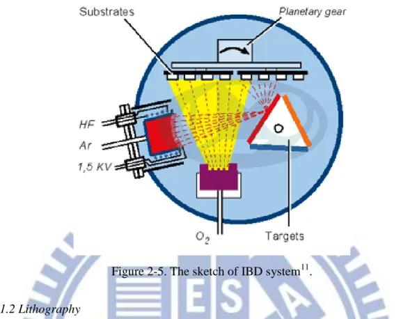
In our research, the NiOx and TiOx film were prepared by the ion beam sputtering (IBS). Figure 2-5 shows the sketch of IBD. In the deposition process, the high energy ions beam was of electron cyclotron resonance (ECR) provided by microwave generator. With the controlling of electric field by microwave, the ECR produced high energy ion beam, and the ionization of gas molecule was done in the ion emission process. Then the ion beam rush to the target and the atoms of target will be hit out by this ion beam, and they will fly to the substrate to coat on the substrate surface. Moreover, with the addition of oxygen gas flow, we can prepare different oxygen content sample with different oxygen flow ratio.
17
Figure 2-5. The sketch of IBD system11.
2.1.2 Lithography
In the micro fabrication, photolithography is used to define the geometric pattern. Coating, exposure, and development are three parts of lithography process. Figure 2-6 shows the process flow of lithography. First, the substrate is coated with a light sensitive chemical material, which is called the photoresist (PR). This process is also called the coating. Second, the exposure process uses light to transfer a pattern from a mask to PR on the substrate. The area with light exposure can be removed or kept on the substrate, dependent on the PR character (positive or negative PR). Moreover, this light through mask will pass several lenses and scale down the size to micro or even nano meter scale on the substrate. The minimum size of pattern on the substrate is dependent on the light source. The light with shorter wavelength can define smaller pattern size. Finally, the developer is used to remove the undesired part of PR in the development process. E-beam lithography is another exposure technology without mask. It uses electron beam to define the pattern on the substrate. Although this technology can save the mask price, the process speed is much slower than traditional lithography technology. In our experiment, the both top metal and metal oxide pattern was prepared by JOEL6500.
18
Figure 2-6. The sketch of Lithography process12.
2.1.3 Etching
In the etching process, an aqueous chemical ("wet") or plasma ("dry") is used to remove the uppermost layer without protection. The isotropic wet etching process is used for highly selective material etching process. For example, the etching ratio between silicon oxide (SiOx) and silicon nitride (SiNx) is very high in the phosphoric acid solution. It is usually used to remove the SiNx layer. However, another anisotropic dry etching process is generally used in order to avoid the significant undercutting of profile. Due to its straight profile, most etching processes use dry etching process in the semiconductor fabrication.
Wet etching, the simplest etching technology, requires nothing but a container with a liquid solution that will dissolve the material. Because this process uses liquid solution, the isotropic etching process can’t be avoided. In this process, the protection layer becomes highly important because it can avoid the undercutting issue. Figure 2-7 shows the anisotropic and isotropic etching process. The isotropic etching process inevitably induces the undercutting issue.
19
Figure 2-7. The sketch of etching process13.
Dry etching, the anisotropic etching process, is usually used for general semiconductor fabrications. The dry etching process uses the plasma with chemical gas to remove the part without protection. Figure 2-8 depicts the dry etching process. Because the plasma has one way direction, the dry etching can avoid the undercutting issue. The anisotropic dry etching profile was shown in figure 2-7.
Figure 2-8. The sketch of dry etching process14.
2.1.4 Chemical mechanical Polishing (CMP)
Figure 2-9 delineates the CMP process. In this process, the top material on wafer surface will react with the chemical solution, and then the mechanical polish is used to remove the material on wafer surface. Another purpose of this process is to make the wafer surface smooth. In the Cu interconnector process, the CMP process is used for the Cu material removal because Cu can’t be removed by etching process.
13
http://www.el-cat.com/silicon-properties.htm
20
Figure 2-9. The sketch of CMP process15.
2.2 Layout
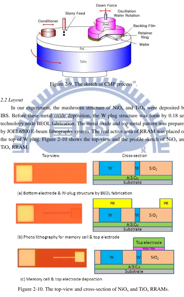
In our experiment, the mushroom structure of NiOx and TiOx were deposited by IBS. Before these metal oxide deposition, the W plug structure was form by 0.18 um technology node BEOL fabrication. The metal oxide and top metal pattern was prepared by JOEL6500 E-beam lithography system. The real active area of RRAM was placed on the top of W plug. Figure 2-10 shows the top-view and the profile sketch of NiOx and TiOx RRAM.
Figure 2-10. The top-view and cross-section of NiOx and TiOx RRAMs.
21
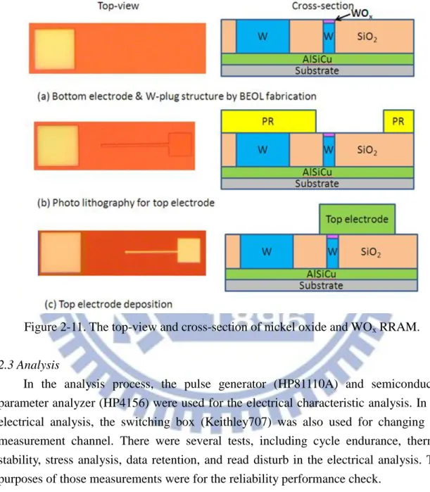
However, the WOx RRAM was formed on the top of tungsten plug by using plasma oxidation process. After this oxidation, the E-beam lithography was used to define the area of top electrode, and then we remove the other part to form the top electrode. The top-view and cross-section of W-based RRAM were shown in figure 2-11.
Figure 2-11. The top-view and cross-section of nickel oxide and WOx RRAM.
2.3 Analysis
In the analysis process, the pulse generator (HP81110A) and semiconductor parameter analyzer (HP4156) were used for the electrical characteristic analysis. In the electrical analysis, the switching box (Keithley707) was also used for changing the measurement channel. There were several tests, including cycle endurance, thermal stability, stress analysis, data retention, and read disturb in the electrical analysis. The purposes of those measurements were for the reliability performance check.
For material analysis, the x-ray photoelectron spectroscopy (XPS) was used for the compositional analysis and profile analysis. The transmission electron microscopy (TEM) was used for the microstructure observation. Moreover, physical property measurement system (PPMS) was used for the temperature dependence electric character measurement.
22 2.3.1.1 Cycle Endurance Measurement
This cycle endurance measurement is one of the reliability performance tests. The better cycle endurance performance sample indicates the more programming operation times in the cycling process. Figure 2-12 shows the typical cycle endurance test. And the test steps are as follows. First, the initial resistance of memory cell was measured by HP4156. Second, the switching box (Keithley707) changes the channel to pulse generator (HP81110A) and then gives a pulse voltage to switch the resistance state. Third, return the channel to read the resistance state again. Finally, switch the channel to pulse generator again and apply a pulse voltage to switch back the resistance state. Repeating these previous processes is the cycle endurance test.
Figure 2-12. The 2 bits/cell cycle endurance test of RRAM[36].
2.3.1.2 Thermal Stability Measurement
The thermal stability test is another measurement of reliability performance test. In our thermal stability test, we program the resistance state to both high and low resistance state and then put those two resistance state samples in high-temperature (above 85℃) oven for long time baking. In the baking process, those samples was take out from oven to confirm the resistance state at room temperature for a period then put back to oven for long time baking. With this repeatedly and period test, we can observed the thermal stability performance. Figure 2-13 shows the typical thermal stability test. The memory cell exhibits better thermal stability performance with the higher baking temperature or long baking time test.
23
Figure 2-13. The typical thermal stability test[37].
2.3.1.3 Stress Test
In the stress test, we use the pulse generator to prove a long time stress, and the resistance is measured by HP4156 after the stress-applied bias. In this stress process, the direction of stress voltage is opposite to the switching voltage. For example, if the switching bias is positive voltage, the stress bias is the negative voltage. If the switching bias is negative voltage, the stress bias is the positive voltage. Figure 2-14 shows the typical stress test of RRAM. It shows the influence of applying a stress voltage on the resistance state.
24 2.3.1.4 Data retention Measurement
Before this data retention test, the switching voltage formed all resistance states. After the resistance switching process, HP4156 was used to detect the resistance of memory cell for a period of time. By means of this periodicity reading and waiting process, we can observe the data retention performance in this test. Moreover, the reading voltage of this data retention test must be small because the memory cell may be damaged by large voltages in the reading process. With this long time resistance reading process, we can obverse the data retention performance. Figure 2-15 shows a typical data retention test of 2bits/cell RRAM device. In this figure, all four-resistance states keep the same resistance value more than 104 src.
Figure 2-15. The data retention test of 2 bits/cell RRAM device[29].
2.3.1.5 Read Disturb Measurement
In the read-disturb performance test, it is similar to the data retention test. Before the read-disturb test, the switching voltage formed all resistance states. The different part with the data retention test is the waiting time. In this test, there are only reading processes in this measurement. With these repeating resistance reading process, we can observe the read-disturb performance of memory cell. Moreover, the small reading voltage is used to avoid damaging the memory cell in the test process. Figure 4-16 shows the typical read-disturb performance test. In this figure, The “On” state is influence by the reading voltage, and the “Off” state keeps the same value in the read-disturb process.
25
Figure 2-16. The typical read disturb test of RRAM device[37].
2.3.2.1 XPS Analysis
X-ray photoelectron spectroscopy (XPS) is a quantitative spectroscopy technology to determine the elemental composition, empirical formula, and electronic state of elements. It is the use of low-energy X-ray source as the excitation source and through the analysis of samples with a characteristic energy of emitted electrons to achieve the purpose of analyzing the chemical composition; that is an ample surface analysis technology. Figure 2-17 shows the construction of XPS. XPS analysis is made into the X-ray beam; the atoms interact with the sample surface after the electronic excitation of atomic inner-shell ionization to detect the sample composition and structure. This is the characteristic X-ray excitation, and the electron here is called ionization photoelectron. Because of the specific wavelength of the X-ray, its energy is known, and the electron binding energy can be calculated by Eq.(2-1).
)
(
photon kinetic bindingE
E
E
………. (2-1)Here, Ebinding is the binding energy of electron, Ephoton is the energy of the X-ray photon, Ekinetic is the kinetic energy of the electron as measured by the instrument, and ψis the work function of the spectrometer. The XPS spectrum can be observed by using binding energy as X-axis and relative intensity as Y-axis. With this spectrum, we can get the informant of samples with elemental composition and chemical state. XPS is the most useful for chemical analysis, and it is also call “electron spectroscopy for chemical analysis” (ESCA).
26
Figure 2-17. The sketch of XPS16.
2.3.2.2 TEM Analysis
Transmission electron microscope (TEM) uses high-energy electron beam (about 100keV ~ 1MeV) through the thin samples (below 100nm), and various structure within the thin samples have different degrees of scattering. Scattering of electrons by means of different routes goes through the subsequent combination of lens aperture lens, forming the contrast images of light and dark, and the microstructure of these images is shown with the fluorescent plate. Therefore, transmission electron microscopy analysis of thin samples is acquired through transmitted electron or elastic scattering electron, or diffraction pattern microstructure, and thus resolves the structure of the thin samples and the crystal structure. Figure 2-18 shows the construction of TEM.
Moreover, the selected area electron diffraction (SAED) in TEM instrument is also can be used to check the sample structure. The SAED principle is in that thin crystal sample, the high-energy parallel ray electron beam can go through this thin sample. In this case, electron is the corresponding volatility, rather than the particle nature. As the energy of the electron wavelength is nanometers in length, and the wavelength is relatively much larger than the spacing between atoms, the atoms are arranged in this electron diffraction grating. This means that a portion of the wavelength will be scattered out of a particular point of view (different parallel surfaces) and will decide the crystal of the sample.
27
Figure 2-18. The sketch of TEM17.
2.3.2.3 PPMS Measurement
The temperature dependent electric character data was analyzed by the PPMS system PPMS. The cooling system uses the liquid helium (He) to cool the measurement system, and the minimum temperature is about 4K. The temperature range is between the room temperature and 4K. In the cooling process from room temperature to 4K, we can observe the resistance change in this cooling process.
28 Chapter 3 : Principles
In recent years, many researches study the resistive switching mechanisms of novel RRAM. According to the result of these studies, we discuss several important physics parameters which influence the performance of RRAM. These physics parameters including cell thickness[38], cell size[39], doping material[40] , electrode[41], density of oxygen vacancies, and electric field[38,42]. Moreover, the RRAM performance can also be improved with modified operation process[36,43,44]. By applying suitable device structure and modified operation to potential materials, the RRAM device performance shows much improvement in the last ten years.
For the electric characteristics analysis of RRAM, many researches on different materials elucidate the electron transport mechanisms of both high and low resistance states follow various conduction mechanisms, such as metallic transportation[20], Schottky emission[45], tunneling, space-charge-limited-current (SCLC)[46], Frenkel-Poole emission[47-49], Trap-assisted-Tunneling (TAT)[50], electron hopping transportation[20], and so on.
Moreover, for the resistive switching mechanism studies, most of the literatures indicate the conducting filament[51-53] mechanism related to oxygen-vacancy[54,55]. Also, various models, such as stochastic model[56], two-variable resistor model[46,57], compact model[58], thermal dissolution model[48,59], rupture ball model[38], etc., were proposed to explain the resistive switching phenomenon in their researches.
In order to show a specific RRAM profile for readers, we introduce the basic resistance switching characteristics and nomenclature, electron transportation mechanism, resistance switching mechanism and model, key physics parameters and modified operation process in this chapter.
3.1 Resistance Switching Characteristics and Nomenclature
Before the introduction of RRAM principle, we describe the basic resistance switching characteristics including bipolar, unipolar, and nonpolar operations. Also, we discuss the basic resistance switching nomenclature, including forming process, set (programming) process, reset (erasing) process, forming voltage , set voltage (current), reset voltage, HRS (reset state), LRS (set state), resistance window (on/off ratio), dc voltage (current) sweep, and pulse switching in this section.
3.1.1 Bipolar, Unipolar, and Nonpolar Operations
For the resistance switching phenomenon in RRAM, bipolar and unipolar are the two major operational methods in the bistable resistance switching process. In earlier researches at 1970s, the most common resistance switching phenomenon of RRAM displays the bipolar operation. It means that the resistance state depends on the polarity

![Figure 2-12. The 2 bits/cell cycle endurance test of RRAM [36] . 2.3.1.2 Thermal Stability Measurement](https://thumb-ap.123doks.com/thumbv2/9libinfo/8748501.205394/36.892.148.715.386.878/figure-bits-cycle-endurance-rram-thermal-stability-measurement.webp)
![Figure 2-15. The data retention test of 2 bits/cell RRAM device [29] . 2.3.1.5 Read Disturb Measurement](https://thumb-ap.123doks.com/thumbv2/9libinfo/8748501.205394/38.892.138.738.252.829/figure-data-retention-rram-device-read-disturb-measurement.webp)
![Figure 3-24. Measured and calculated relationships [56] of NiO film between the set/reset voltage and (a) the sweep rate or (b) the set/reset transition times](https://thumb-ap.123doks.com/thumbv2/9libinfo/8748501.205394/61.892.196.751.635.1105/figure-measured-calculated-relationships-reset-voltage-sweep-transition.webp)
![Figure 3-32. The simulated I-V curves of bipolar RRAM by compact model [58] .](https://thumb-ap.123doks.com/thumbv2/9libinfo/8748501.205394/68.892.161.728.106.1040/figure-simulated-i-curves-bipolar-rram-compact-model.webp)