2004
IEEE
Asia-Pacific Conference on Advanced System Integrated Circuits(AP-ASIC2004)/ Aug. 4-5, 20048-2
A Low Phase Noise Wide Tuning Range CMOS Quadrature VCO
using Cascade Topology
Chao-Shiun Wang, Shiau-Wen Kao* and Po-Chiun Huang**
NTU-MTK Research Wireless Lab., National Taiwan University, Taipei, Taiwan
*SoC Technology Center, Industrial Technology Research Institute, HsinChu, Taiwan
**Dept. Electrical Engineering, National Tsing Hua University, HsinChu, Taiwan
Abstract - A new fully integrated 2.4CHz CMOS quadra-ture voltage control oscillator (VCO) is presented. It achieves low phase noise at quadrature outputs using the proposed cascade coupling topology. Digitally-controlled capacitor bank is designed for wide tuning range from 2.4 to 2.9GHz.
By a standard 0.25pm single-poly CMOS process with thick top metal, total power consumption of two VCO cores and burners for generating quadrature signal are 6mA and 12mA
respectively. Measured phase noise at lMHz offset from the center frequency is -1l4dbdHz.
1. INTRODUCTION
The era of portable personal communication systems is expanding in an unprecedented fashion and rapidly be-
- coming a part of daily lives. The highly integrated single chip transceiver is developed to reduce cost, power con- sumption and size. Recently, quadrature conversion trans- ceiver is more popular due to its flexibility and high inte- gration. In the design of these transceiver systems, a major challenge is the generation of quadrature local oscillating (LO) signal. Higb phase accuracy, good gain matching and low phase noise quadrature LO signal is required [I]. Several circuits RC phase shift network and poly-phase network methods are widely used in transceiver to gener- ate quadrature LO signals. But they have restrictions in phase accuracy and gain matching since the inaccuracies in actual values of R and C. Their noise performance and driving capability do not fulfill the system requirements in most cases. Divided-by-two is another approach. But the oscillator and divider have to work at the double canier frequency, which is either difficult to design or even hun- gry on power. Multi-stage VCO, like ring-type structure, is a possible way to get quadrature phase output, if its stage number is even. Ring-type VCO however exhibit poorer phase noise performance compared with the LC- type VCO. In general cross-coupled LC-tank VCO is be- lieved to perform low phase noise for quadrature signal generation.
0-7803-8637-X/04/$20.00~2004 IEEE.
This work demonstrates a CMOS quadrature VCO for low power operation in the 2.45GHz range. Its tuning range has to cover 20% to against process variation. The symmetrical spiral inductors and differential varactors are all on chip to achieve highly integration. A prototype is fabricated in 0 . 2 5 ~ single-poly with thick top metal CMOS process.
The paper is organized as following. Section 11 dis- cusses the design considerations of the proposed quadra- ture VCO. Section 111 descripts the VCO tuning circuits. Section IV presents measurement results. Some conclu- sions of this design are offered in section V.
II. PROPOSED QUADRATURE VCO Typical quadrature signal generator is shown in Fig. 1. It uses two cross-coupled VCOs to generate pi2 phase dif- ference between 1 (in-phase signal node) and Q (quadra- ture-phase signal node) at resonant frequency [2]. Even so. this topology associates some drawbacks that limit quad- rature VCO phase noise performance. Firstly, the coupling devices consume additional current. Moreover, the noise ofcoupling devices is easy to arise at outputs [3].
T
I-
Q+
p
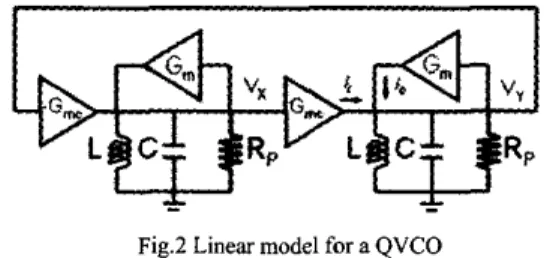
Fig.1 Typical cross coupled quadlature VCO Fig.2 introduces a linear model for the typical quadra- ture VCO, where G, represents the transconductance of2004 IEEE Asia-Pacific Conference on Advanced System Integrated Circuits(AP-ASIC2004)/ Aug. 4-5,2004
the negative-resistance pair, and G , is the transconduc- tance of the quadrature signal coupling pair. The limiting factor in maximum oscillation frequency is the parasitic phase shift in transconductance G,, of the linear model. Thus, the oscillation frequency can be descried as follow- ing:
wherep =tan(90"- e)and B =tan~'(lIQl/lII
1)
[4]. 0 is pro- portional to the coupling factor.Fig.2 Linear model for a QVCO
Fig. 3 is the combined phaser diagram of the output voltages Vx and Vy and the currents in the quadrature stage i, and i,. This diagram shows that, in conventional quadrature-coupled LC oscillators, Vx and Vv phases are shifted by p/2 when il and iQ are equaled. It is noteworthy that the phase and amplitude accuracy of the quadrature outputs is proportional to coupling factors.
.
.-
Fig.3 Combine phasor diagram of output voltage Vx and V, The phase noise of typical quadrature VCO is calcu- lated by using the linear model outlined in [ 5 ] . The phase noise can be depicted as
where /OX is the carrier frequency, ,;&a, is the squared rms carrier current and QP is the quality factor of the reso- nator at the resonance frequency. As expected, the phase noise is degraded for higher coupling ratio.
In order to get good phase-noise performance and good image rejection, a cascade-connected topology is adopted
[3]. This structure can force two VCO cores to generate
currents with correct phase shift. The associated quadra- teure phase error will be greatly reduced a s the error is almost independent for the coupling stage transconduc- tance. Besides that, this cascade can provide better isola- tion between the two oscillator cores.
Fig.4 shows the schematic diagram of the proposed VCO. It consists of two identical LC oscillators MI-M8, which inject-lock to each other through n-MOS coupling devices M9-Ml2. M9-MI2 are cascading to the core, to
alleviate the problems associated with the conventional approaches such as Fig. 1.
Fig.4 Proposed quadrature VCO schematic In the VCO core p-MOS Ml-M4 and n-MOS M5-MX form two cross<oupled pairs. These cross-coupled MOS pairs act like negative resistors with their transconduc- tances as:
where G , is the device transconductance in the cross- coupled pairs,
%
is the parallel resistance of the LC tanks at resonance frequency, L and C is the inductance and capacitor, Qmk is the quality factor of the LCtanks.
Parallel p-MOS and n-MOS differential pair achieves larger oscillation amplitude than n-MOS-only, which re- sults in a better phase noise performance for a given tail current. Symmetric rise and fall time are designed care- fully to reduce the IRnoise upconversion [ 5 ] . In addition, large tail capacitors C l and C2 are added to provide a low impedance path to AC ground at harmonic frequencies. This technique can attenuate high frequency noise coming of tail current, to further improves the phase noise per- formance of the whole VCO.
2004 IEEE Asia-Pacific Conference on Advanced System Integrated Circuits(AP-ASIC2004)i Aug. 4 - 5 2 0 0 4
Fig.5 shows the symmetrical inductor's layout and the cross section of the differential varactors. These fully dif- ferential structures improve the tank's quality factor, re- duce chip area, and keep symmetry to the oscillator cir- cuits. All these will help to reduce flicker noise modula- tion.
. .
Vin-
"-well
(b)
Fig.5 (a) Symmetric spiral inductor layout (b) The cross section of differential vxactors
Ill. DIGITAL TUNMG TECHNIQUE
On-chip varactor can only provide tuning range of IOOMHz, or 4% of operation frequency. To extend the tuning range to cover the process spread, Fig. 6 is the pro- posed digital tuning technique, without increasing the gain of VCO. In this design, digital tuning is used to push the VCO to the lock-in range of synthesizer. The analogue tuning will do the following phase-locking process.
For tuning digitally, both VCO outputs are loaded with differential 5bit binary-weighted switched-capacitor banks. Each capacitor ONiOFF state is controlled by another Sbit binary-weighted decoder. Switch in capacitor bank adopts complementary control to prevent the capacitor floating when it is on OFF state. In order to maintain same quality factor Q for each setting, NMOS switch widths also need to be binary-scaled. These digitally-tuned capacitor banks equate for an additional 5OOMHz tuning range according
to
simulations and measurement.~
T, R.
Fig.6 Digital tuning with binaly-weighted capacitor bank
IV. MEASUREMENTS
The die microphotograph is shown in Fig.7. The area is 7 0 0 ~ x 7 0 0 ~ , including VCO and binary weighted control decoder. The die was mounted in a standard plas- tic, low cost, TSSOP package. Each single buffer output is ahout -10dBm under 500 measurement system. The com- plete quadrature VCO with buffers draws 18mA from a single 2.5" supply. The oscillator operation range is from 2.4GHz to 2.5GHz, when the control voltage is swept from 0.5V to 2V and digital tuning word is '00000'. This means the analog tuning range is 5% under the center fre- quency of 2.45GHz. The maximum digital tuning word '1 I 1 1 I ' sets the VCO with a maximum frequency of 2.9GHz, which yields a 20% tuning range.
Fig.7 A die microphotograph of quadrature VCO
In-phase output phase noise are presented in Fig.11, the quadrature output has a similar phase noise character- istic. The QVCO has a phase noise of -90dBciHz at lOOkHz offset, -1OldBciHz at 300kHz offset, - I I2dBciHz at lMHz offset from 2.4GHz to 2.9GHz.
2004 IEEE AskPacific Conference on Advanced System Integrated Circuits(AP-ASIC2004)/ Aug. 4-5,2004
Oscillator Frequency
Phase Noise @ I MHz offset Phase Ermr Amplitude Error
Tuning Range
". ".
Fig 8 QVCO output spectmm at 2 4GHz
2.4CHz
-
2.9GHz 20% -Il4dBc/Hz <IS? < IdB ... ..".".,*l.n?u*l-D .: "1 ... ...Power Consumption (WIO Buffer)
l
o L , . * I n ~ m ~
I, , . , , , , , , ,
---
Fig.10 Measured digital tuning range of QVCO The phase error over the whole tuning range was less than 1.5 degrees. The amplitude error was less than 1dB. Image rejection ratio (IRR) therefore can be better than 50dB. * -.-e,- -.-e-
-.-*
' Y I U-
s..
*..-.~*-.-L...-*m... .
...
f i
E:
- -
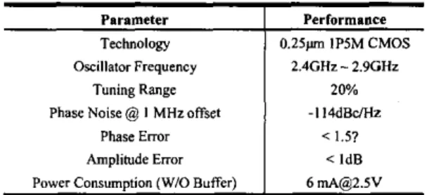
The measurement results of the quadrature VCO with output buffers are summarized in Table 1.
Parameter
I
PerformanceTechnology
1
0 . 2 S p IPSM CMOSTable 1 Performance summary of the proposed QVCO.
V. CONCLUSION
Cross-coupled structure is widely used for quadrature VCO design. Cascade topology adopted is proven to pos- sess lower phase noise characteristic rather than the con- ventional parallel-coupled configuration. Based on this insight, a monolithic 2.4GHz CMOS quadrature VCO using 0 . 2 5 ~ technology has been realized. Several tech- niques like balance N- and P- crosscoupled structure and bypass tail current harmonics are incorporated to m e r reduce output phase noise. Digitally switched capacitor bank helps on a wide tuning rang. Image rejection ratio is
expected to be better than 5OdB as the gain and phase mismatch is small. The phase noise is -114dBdHz at I MHz offset over the whole tuning range. This quadra- ture VCO achieves low phase noise under low power dis- sipation.
REFERENCES
[ I ] Behzad Razavi, "RF Microelectronics," Prentice Hall PTR. , 1998.
[2] A. Rofougaran er a/., "A 900MHZ CMOS LC-oscillator with quadrature outputs," in IEEE int. Solid Srare Circuits ConJ (ISSCC) Dig. Tech. Papers, pp. 392-393, 1996. [3] P. Andreani er al., "Analysis and Design of a 1.8-GHz
CMOS LC Quadrature VCO," in IEEE J. Solid Stare Cir- cuits, ~ 0 1 . 3 7 , ~ ~ . 1737-1747,Dec.. 2002.
[4] J. Van der Tang er al., "Analysis and Design of an Opti- mally Coupled 5-GHz Quadrature LC Oscillator," in IEEE J. SolidSrare Circuits, vo1.37, pp. 1737-1747, Dec., 2002.
R. Apancio er al., "A Noise-Shifting Differential Colpins VCO," III IEEE J. Solid Stare Circuits, vo1.37, pp. 1728- 1136, Dec., 2002..
[ 5 ]
. . .
Fig.11 Measured phase noise through whole tuning range