行政院國家科學委員會專題研究計畫 期中進度報告
新型高效率微致動器及其應用在微機電與微光機電系統之
研究(2/3)
計畫類別: 個別型計畫 計畫編號: NSC94-2212-E-009-005- 執行期間: 94 年 04 月 01 日至 95 年 03 月 31 日 執行單位: 國立交通大學機械工程學系(所) 計畫主持人: 徐文祥 計畫參與人員: 林正軒 葉昌旗 鍾君煒 楊涵評 報告類型: 精簡報告 報告附件: 國際合作計畫研究心得報告 處理方式: 本計畫可公開查詢中 華 民 國 95 年 1 月 29 日
行政院國家科學委員會補助專題研究計畫
行政院國家科學委員會補助專題研究計畫
行政院國家科學委員會補助專題研究計畫
行政院國家科學委員會補助專題研究計畫
□
□
□
□成果報告
成果報告
成果報告
成果報告 ▓
▓
▓期中進度報告
▓
期中進度報告
期中進度報告
期中進度報告
新型高效率微致動器及其應用在微機電及微
光機電系統之研究(2/3)
計 畫 類 別 : ■ 個 別 型 計 畫
□ 整 合 型 計 畫
計 畫 編 號 : NSC 94 - 2212 - E - 009 - 005 -
執行期間: 94 年 4月 1日至 95 年 3 月 31 日
計畫主持人:徐文祥
共同主持人:
計畫參與人員:
林正軒 葉昌旗 鍾君煒 楊涵評
成果報告類型(依經費核定清單規定繳交):■精簡報告 □完整報告
本 成 果 報 告 包 括 以 下 應 繳 交 之 附 件 :
□
赴
國
外
出
差
或
研
習
心
得
報
告
一
份
□ 赴 大 陸 地 區 出 差 或 研 習 心 得 報 告 一 份
□ 出 席 國 際 學 術 會 議 心 得 報 告 及 發 表 之 論 文 各 一 份
■國際合作研究計畫國外研究報告書一份
處理方式:除產學合作研究計畫、提升產業技術及人才培育研究計畫、列
管計畫及下列情形者外,得立即公開查詢
□涉及專利或其他智慧財產權,□一年□二年後可公開查詢
執行單位:國立交通大學機械系
中 華 民 國 95 年 1 月 16 日
一 一 一 一、、、、中文摘要中文摘要中文摘要中文摘要 本計畫 本計畫 本計畫 本計畫提出提出提出提出一一一一串聯式雙層板串聯式雙層板串聯式雙層板串聯式雙層板微熱致動器微熱致動器微熱致動器微熱致動器,,其原理是串,,其原理是串其原理是串其原理是串接數個基本微熱致動器接數個基本微熱致動器接數個基本微熱致動器接數個基本微熱致動器,,,累積其位移而產生,累積其位移而產生累積其位移而產生累積其位移而產生 垂直方向之大位移量 垂直方向之大位移量垂直方向之大位移量 垂直方向之大位移量。。。每個基本微熱致動器包含兩種雙層板結構及一個拘束樑。每個基本微熱致動器包含兩種雙層板結構及一個拘束樑每個基本微熱致動器包含兩種雙層板結構及一個拘束樑每個基本微熱致動器包含兩種雙層板結構及一個拘束樑。。。。與同尺寸下之傳統雙與同尺寸下之傳統雙與同尺寸下之傳統雙與同尺寸下之傳統雙 層板微熱致動器相比 層板微熱致動器相比層板微熱致動器相比 層板微熱致動器相比,,,此設計可提供較大位移,此設計可提供較大位移此設計可提供較大位移此設計可提供較大位移,,,,製作上製作上是利用面型加工技術製作製作上製作上是利用面型加工技術製作是利用面型加工技術製作是利用面型加工技術製作,,,,材料主要由鋁及多材料主要由鋁及多材料主要由鋁及多材料主要由鋁及多 晶矽構成 晶矽構成晶矽構成 晶矽構成。。。在此用。在此用在此用4在此用444個基本單元來驗証設計個基本單元來驗証設計概念個基本單元來驗証設計個基本單元來驗証設計概念概念概念,,,,面積約面積約面積約面積約510 x 400 µµmµµ 2。。。。由實驗發現由實驗發現由實驗發現由實驗發現在在4.5V時在在 時時,時,,,可提可提可提可提 供約 供約供約 供約22.5 22.5 µ22.5 22.5 µµm垂直µ 垂直垂直垂直位移位移位移位移。。操作。。操作溫度並經由熱像儀量測操作操作溫度並經由熱像儀量測溫度並經由熱像儀量測,溫度並經由熱像儀量測,,4.5V,4.5V4.5V時約為4.5V時約為147時約為時約為147147147℃℃℃℃,,,,10V10V10V10V時仍低於時仍低於400時仍低於時仍低於400400400℃℃℃,℃,,與,與與與 ANSYS ANSYSANSYS ANSYS電腦膜擬結果相當接近電腦膜擬結果相當接近電腦膜擬結果相當接近電腦膜擬結果相當接近。。。。 英文摘要 英文摘要 英文摘要 英文摘要
Here a cascaded bimorph actuator is proposed by integrating several novel actuation units to accumulate the vertical displacements. Each actuation unit comprises two types of bimorph beams and a constraint bar, and both beams will stretch outward with respect to the constraint bar while heating. In comparison with other three conventional bimorph actuator designs at the same device size, it is shown that the proposed design can provide larger vertical
displacement. The proposed cascaded bimorph actuator is fabricated by surface
micromachining technique and released by XeF2 silicon isotropic etching. Whole suspended
structure consisting of the polysilicon and the aluminum is around 510 x 400 µm2 with four actuation units. The resistance is about 650 Ω. In testing, the fabricated device is shown to provide reversible vertical displacement of 22.5 µm at 4.5 V, and the operating temperature is measured by an infrared thermal microscope (InfraScope II, QFI). The calibrated maximum temperatures are compared with simulated results by ANSYS 6.0 in good agreement. It is found that the maximum temperature is 147 °C when the input voltage is 4.5 dc volts, and the maximum temperature is below 400°C even at 10 V.
Keywords: thermal, bimorph, cascaded, actuator, heating region
二 二二
二、、、計劃緣由、計劃緣由計劃緣由與目的計劃緣由與目的與目的與目的
A micro actuator with larger output force and displacement at a compact size is always the research goal in MEMS area. A single micro actuator usually can provide only limited output force and displacement. Therefore, proper integration of several basic actuators into an arrayed structure becomes an attractive way to magnify the output. In electro-thermal microactuators, thermal bimorph effects have been applied widely to microactuators for large deflections and moderate forces under IC-level low driving voltages. One typical structure type used in thermal bimorph actuation is the cantilever structure. Thermal bimorph structures with beam and membrane types are also found in many applications .
However, in thermal bimorph actuators, larger displacement usually requires longer beam length, which will occupy larger device size and may be limited by the releasing method in fabrication process. In order to further magnify the displacement in a compact size, here a cascaded electro-thermal bimorph micro actuator is proposed. Comparing to conventional bimorph actuators, the proposed micro drives are expected to provide larger displacement at the same device size. Silicon-based surface micromachining technique will be used to fabricate the device, and the thermal and mechanical behaviors of the device will be investigated experimentally and analytically.
三 三 三
三、、、、 研究方法研究方法研究方法研究方法
PRINCIPLE AND CONCEPT DESIGN
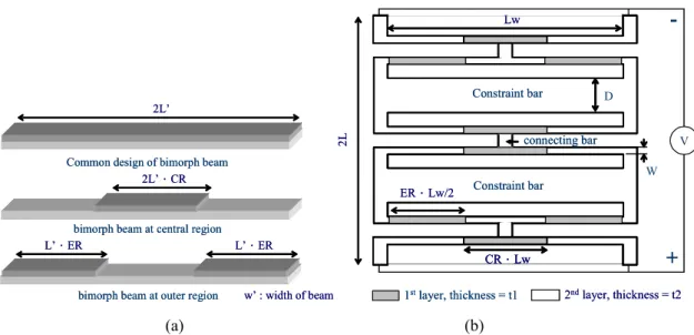
Figure 1(a) illustrates three conventional bimorph structures with different heating regions, full bimorph type, bimorph in central region type, and bimorph in edge region type, respectively. From our previous studies, when the upper layer has larger coefficient of
thermal expansion (CTE) and two ends of the bottom layer are fixed, the full type and central region type will provide upward deflection while heating. The edge region type will generate downward deflection on the other hand.
The proposed cascaded bimorph actuator (CBA) is formed by connecting several basic actuation units in serial. Each actuation unit comprises two bimorph structures and a constraint bar. Two bimorph structures which are edge region type and central region type to generate downward and upward deflections, respectively, are arranged in transverse way. Connecting these two different bimorph beams and a constraint bar longitudinally can form the basic actuation unit. While heating, the constraint bar will limit the transverse thermal expansions of bimorph beams, then both beams will stretch upward or downward with respect to the constraint bar. Since the vertical displacement of bimorph beams depends on transverse length, not the longitudinal length, when several actuation units are connected in serial to form a cascaded structure, as shown in Fig. 1(b), the outward displacements from each actuation unit can be accumulated to provide a larger vertical displacement with a smaller longitudinal size.
Figure 1 (b) illustrates the design of two actuation units with two extra central-type bimorph beams, the definitions of geometrical parameters are also shown. The upper layer, denoted as 1st layer, has larger CTE than the bottom heating layer denoted as 2nd layer. The length and width of the beam are denoted by Lw and W, respectively. The longitudinal length of the cascaded bimorph actuator is denoted by 2L. The symbols ER and CR represent the length ratios of bimorph parts to the whole length of edge region type and central region type, respectively.
SIMULATIONS
Here finite element software ANSYS® 6.0 is used to investigate the thermal and mechanical behaviors of the proposed device. In order to realize the advantage of the proposed design, deflections of three conventional designs with different heating regions of bimorph beams in Fig. 1(a) are first used to compare with the proposed CBA through simulations under different elevated temperature. As shown in Fig. 2 , with the same dimension and materials, the full type and the central region type will generate upward displacement. The edge region type will exhibit downward displacement, and the proposed CBA in Fig. 1(b) can provide the largest vertical displacement owing to the accumulations from each actuation unit. Also, the deflection of full type is larger than that of central heating region type.
For further investigation, CBA consisting of four actuation units and two extra bimorph beams is used, temperature distribution is also investigated. Since the proposed micro actuator is complicated, and the constraint bars in the proposed micro actuator may consume thermal energy through heat conduction and affect not only heat transfer but also output displacement. To analyze this complicated structure, sequentially coupled analysis technique is used in simulation, including two steps. The first step is the nonlinear electro-thermal analysis with 3-D 69-solid element, and the second step is the nonlinear thermal stress analysis with 3-D 45-solid element. Since the device is symmetric, the finite element model is built in half for computational efficiency. The modeling is fully surrounded by air and the mesa of silicon substrate, which is built beneath the electrical contact pad. Aluminum and polysilicon are selected respectively as the upper and bottom layers of CBA, respectively due to the large difference in CTE and our fabrication capability. Also, thin thermal dioxide is used as the isolation of electro-thermal layer when the polysilicon also acts as the electrical heating layer. Table 1 lists the material properties used in simulation.
In electro-thermal analysis, reference temperature is set at 25°C on surface of silicon substrate and the ambient air. Electric potential loads are applied on the top surface of the contact pad and on the symmetrical plane of the connecting bar. Both conduction and convection of heat transfer are considered in analysis. Therefore, the thermal conductivity and specific heat of the structure materials and air are considered. In addition, the reflow of aluminum layer will occur when the temperature is higher than 400°C, therefore the cases with maximum operating temperature of CBA below 350°C are simulated. Figure 3 shows the effect of air gap between the suspended structure and the silicon substrate is investigated first. It is found that the output displacement and the maximum temperature will increase with the air gap owing to the tougher thermal conduction through thicker air gap. Figure 4 shows the output displacement under different thickness ratios between Al layer and polysilicon layer, where the polysilicon and thermal dioxide are set as 1.5µm and 0.2µm, respectively. Thickness ratio of 0.8 provides the largest displacement. The output displacement under different bimorph length ratios ER and CR for outer region and central region types, respectively, are shown in Fig. 5. The optimal length ratios for central and edge types are all 0.5. The width ratio between the constraint bar and the bimorph beam, D/W, is also investigated. In thermal simulation, as shown in 6, higher temperature can be induced at smaller D/W, because of less heat dissipation through a narrower constraint bar. In general, higher temperature at bimorph beams, i.e. smaller D/W, will generate larger vertical displacement with fixed ends, as shown in Fig. 6, output displacement decreases from D/W=2.0 to 6.0. However, a narrow constraint bar will thermally expand more easily due to high temperature, which will seriously damage the boundary condition of bimorph beams to cause vertical output displacement decreasing, that is what happens in Fig. 6 for D/W= 0.5 and 1.0. Therefore the optimal D/W ratio can be found as 2.0, where largest displacement is achieved without reaching highest maximum temperature.
FABRICATION PROCESS
In this work, the cascaded bimorph actuator is fabricated by surface micromachining and released by vapor phase etching with xenon diflouride, XeF2 (X3 Series in Xetch®).
Furthermore, the proposed actuator is consisted of the aluminum and the polysilicon as two major layers. The thermal oxide and the AZ4620® thick photoresist are used to cover and protect the whole device during the silicon isotropic etching. Plasma-enhanced chemical vapor deposition (PECVD) oxide is used here to be an isolated layer for the isolated electricity between the aluminum and the polysilicon layer. This three-mask process is illustrated in Fig. 7.
TESTING
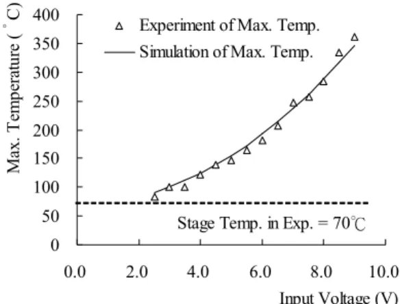
For temperature measurement, Infrared thermal microscope (InfraScope II, QFI) is used here to measure the temperature image of CBA while heating. It provides automated spatial emissive compensation that produces a true temperature of the tested device. The focusing stage is controlled by the computer. The temperature resolution is 0.1°C at 80°C, and the calibrated range is from 30°C to 400°C. Also, the pixel resolution of temperature image is 6 µm at optics percentage of 5X. The fabricated sample is tested on a stage with controlled reference temperature of 70°C. Then two probes, connecting from power supply, are contacted with CBA under different input voltages. Figure 9 shows the measured temperature image at 5 Volts. The locations with the highest temperature can found to be around the middle point and the bimorph structures near the middle two actuation units.
The comparison between simulated and calibrated maximum temperature at different input voltages is shown in Fig. 10 with good agreement. It is found that the maximum
temperature is 147 °C when the input voltage is 4.5 dc volts, and the maximum temperature is still below 400°C even at 10 V.
Displacement test is performed at the stage of the optical microscope, and the deflection is measured by recording the focal length difference when it is focalized on top surface of CBA at different voltages. In experiments, an irreversible deflection of CBA is occurred at applied voltage over 4.7 volts. Figure 11 shows the upward deflection of CBA with four actuation units at 4.5 volts. The measuring points of bimorph beams with central heating region, denoted A and E, have a displacement of around 9.5 µm, and the relative displacement from point B to point A, or point D to point E, is only about 6.5 µm. The maximum displacement happening at point C is about 22.5 µm, which is smaller than we expected. Figure 12 shows the simulated and measured vertical displacement at different input voltages. The mismatch may come from the initial curvature or so-called geometrical imperfection owing to the residual stress in fabricating the bimorph structure. The curved shape of bimorph beam would cause unstable deflecting behavior while heating. In our simulation, the bimorph structure is assumed flat, no initial curvature is considered. Thus, the output displacement of the bimorph structure may deviate from simulation, even with the accurate temperature distribution model.
四、結論
A cascaded bimorph actuator is designed, fabricated, and tested here. The fabricated device is shown to provide reversible vertical displacement of 22.5 µm at 4.5 V, and the calibrated maximum temperatures are compared with simulated results in good agreement. It is found that the maximum temperature is 147 °C when the input voltage is 4.5 dc volts, and the maximum temperature is below 400°C even at 10 V. However, it is found that the measured vertical displacements deviate from the simulation evidently, which may be caused by the curved shape of the bimorph beam. Further investigations on other low-temperature fabrication technique or structure materials may be helpful in future improvement.
五、圖表
bimorph beam at central region
bimorph beam at outer region 2L’
2L’.CR
L’.ER
Common design of bimorph beam
L’.ER
w’ : width of beam bimorph beam at central region
bimorph beam at outer region 2L’
2L’.CR
L’.ER
Common design of bimorph beam
L’.ER w’ : width of beam Constraint bar 2ndlayer, thickness = t2 1stlayer, thickness = t1 V -+ Constraint bar 2 L W D Lw ER.Lw/2 CR.Lw connecting bar Constraint bar 2ndlayer, thickness = t2 1stlayer, thickness = t1 V -+ Constraint bar 2 L W D D Lw ER.Lw/2 CR.Lw CR.Lw connecting bar (a) (b)
Fig. 1 Illustration of the concept design and the geometrical parameter definitions. (a) Bimorph beams with three types of different heating region. (b) Minimum component with two actuation units and two extra bimorph beams.
-10 -5 0 5 10 15 20 0 10 20 30 40 50 Temperature (K) M ax . D is p la ce m en t (u m )
Fig. 2 Simulations with four types of designs under different elevated temperatures. (t1= t2=1.0µm, 2L’=2L=510 µm, Lw = 400 µm, ER=CR=0.5 )
Table 1. Material properties for the simulation model
Material Al PECVD
SiO2
LPCVD
PolySi SC-Si Air
Young’s modulus (GPa) 69 57 150 162 -
Density(kg/m3) 2692 2660 2330 2420 *1.293~0.456
Poisson’s ratio 0.36 0.245 0.28 0.28 -
Resistivity (Ω-cm) 25e-9 - 9e-6 - -
Conductivity (W/m*K) 237 1.1~
2.09 34.0 *146.4~41.8 *0.024~0.056
Specific heat (J/Kg*K) 898.7 176~
223 754 706.4 *1006~1093
CTE (10-6/K) 27.95 0.4 2.33 *2.56~4.10 -
* Temperature dependent - Not used in simulation
0 5 10 15 20 25 30 35 40 45 50 0.0 5.0 10.0 15.0 20.0 25.0 30.0
Air Gap (um)
M ax . D is p la ce m en t (u m ) 0 50 100 150 200 250 M ax . T em p er at u re ( °C )
Simulation of Max. Disp. Simulation of Max. Temp.
0 5 10 15 20 25 30 0.0 0.2 0.4 0.6 0.8 1.0 1.2 1.4 Thickness Ratio (t1/t2) M ax . D is p la ce m en t (u m )
0.1 0.3 0.5 0.7 0.90.1 0.3 0.5 0.7 0.9 0.0 5.0 10.0 15.0 20.0 25.0 M ax . D is p la ce m en t (u m ) CR ER 20.0 -25.0 15.0 -20.0 10.0 -15.0 5.0 -10.0 0.0 -5.0 0 5 10 15 20 25 30 0.0 1.0 2.0 3.0 4.0 5.0 6.0 Ratio of width of Two Beams (D/W)
M ax . D is p la ce m en t (u m ) 0 20 40 60 80 100 120 140 M ax . T em p er at u re ( °C )
Simulation of Max. Disp. Simulation of Max. Temp.
Fig. 5 Effects of length ratios, CR and ER Figure 6 Effect of width ratio, D/W
( a )
( b )
( c )
( d )
Al
Al Poly-SiPoly-Si Resist layerResist layer Mask layer 1Mask layer 1 Mask layer 2Mask layer 2 Si Sub.Si Sub.
Figure 7 Illustration of the fabrication process using surface micromachining and XeF2 isotropic silicon
etching.
0 50 100 150 200 250 300 350 400 0.0 2.0 4.0 6.0 8.0 10.0 Input Voltage (V) M ax . T em p er at u re ( °C )
Experiment of Max. Temp. Simulation of Max. Temp.
Stage Temp. in Exp. = 70℃
Figure 10 Calibrated and simulated (by Ansys 6.0) maximum temperature of the cascaded bimorph actuator with four actuation units under different input voltages
A
A BB CC DD EE
. . . . .
Input Voltage = 4.5 dc volts 0 5 10 15 20 25 A B C D E D ef le ct io n ( u m )
Figure 11 Calibrated displacements of different locations at 4.5 V.
0 5 10 15 20 25 30 35 40 45 0.0 1.0 2.0 3.0 4.0 5.0 6.0 Input Voltage (V) M ax . D is p la ce m en t (u m )
Simulation of Max. Disp. Experimen of Max. Disp.