國
立
交
通
大
學
光電工程研究所
碩
士
論
文
疊合式金氧半太陽能電池之研究
Research on MIS Stacked Solar Cells
研 究 生:李欣育
指導教授:李柏璁 教授
疊合式金氧半太陽能電池之研究
學生:李欣育
指導教授:李柏璁 博士
國立交通大學光電工程研究所碩士班
摘
要
在本篇論文當中,首先我們先分析 n 型與 p 型的金氧半太陽能電池。由於我 們是使用磁控濺鍍機來成長超薄穿隧氧化層,大量的缺陷會在濺鍍過程中被製造 出來。於是我們加入一道氫氣退火的製程,以形成矽氫鍵結的方式來修補矽的懸 空鍵。我們同時也調控氧化層厚度、工作壓力、以及用於載子收集之金屬層的厚 度來達到高開路電壓輸出。 隨後,為了實現疊合式金氧半太陽能電池,我們使用晶圓直接接合的方式來 達到穿隧二極體並對其進行分析。最後再將 n 型與 p 型金氧半太陽能電池整合到 穿隧二極體上,完成疊合式金氧半太陽能電池並量測其光伏特性。量測結果顯示 最好的開路電壓達到 593mV,大於單一接面的金氧半太陽能電池,證明我們所提 出來的結構之可行性以及其用在電解水的潛力
Research on MIS Stacked Solar Cells
student:Hsin-Yu Lee
Advisors:Dr. Po-Tsung Lee
Institute of Electro-Optical Engineering,
National Chiao Tung University
Abstract
In this thesis, the n-type and p-type MIS solar cells are investigated first. Since we use sputter to deposit tunnel oxide as insulating layer, a lot of defects are produced during sputtering. Therefore, we introduce an annealing process in hydrogen atmosphere to passivate Si dangling bonds by the formation of Si-H bonds. We also fine tune the oxide thickness, working pressure, and collecting thin metal thickness to achieve high Voc.
Later, to realize MIS stacked solar cells, we fabricate and investigate the tunneling junction by directly wafer bonding. Finally, we integrate n-type and p-type MIS junctions on bonded sample and measure the photovoltaic properties of MIS stacked solar cells. Consequently, the best Voc we obtain is 593mV, larger than single junction cells, demonstrating that the structure is practical and have its potential to achieve water splitting.
Acknowledgements
首先我要感謝辛苦養育我的父母,沒有你們的支持,我沒有辦法在這衣食無缺的 情況下專心在學業及研究。另外要感謝一些從以前開始就跟我在一起的好夥伴,小蓉、 軒軒、明叡、嘉佑、力綸、啟仁、智猷...等。從大學甚至是從高中以來,大家總 是在我遇到挫折跟問題的時候給我最大的支持跟鼓勵,在成功的時候與我分享成功的 喜悅,進而完成這兩年的碩士學業。 接下來要感謝我的指導教授李柏璁老師,感謝老師在這兩年間對我的指導。在學 術研究上有老師的指引,我最後才能順利完成碩士學業。在人生的規劃上老師。此外 要感謝的是實驗室的夥伴們,盧贊文、張資岳、光揚、家揚、林怡先、蕭逸華、何韋 德...等。特別是博士班學長張資岳,對我的整個論文題目的研究給予很多的幫助 並且共同解決了許多面對到的問題。除此之外,學弟張均隆也常常被我抓去一起做實 驗,對於整個實驗數據也盡了很大的一份力。 最後要感謝經濟部學界科專的計畫補助、交大綠能中心給計畫補助、奈米中心跟 NDL 提供儀器、以及施閔雄老師及余沛慈老師提供儀器,使得我們有足夠的資源能進 行研究。再次感謝所有給予我支持的人,豐富我在交大的這兩年生活,並協助我完成 這篇論文。 2009/08/06 于新竹 國立交通大學 交映樓 401 室
Content
Abstract (in Chinese) ……….……… i
Abstract (in English) ……….…... ii
Acknowledgements ……… iii
Content ……… iv
List of Tables ……… vi
List of Figures ……… vii
Chapter 1
Introduction
1 1.1 Background………11.2 MIS Solar Cells………..1
1.2.1 General Description………..1
1.2.2 First-Generation MIS-IL Solar Cells………3
1.2.3 Second-Generation MIS-IL Solar Cells………4
1.2.4 MIS-n+p Solar Cells (MINP)………6
1.3 MIS Stacked Solar Cells……….………6
1.4 Motivation………..7
1.5 About this work………..8
Chapter 2
Principle of MIS Solar Cells
9 2.1 General Description of Solar Cells………92.2 Transport Mechanism of MIS Junctions………..13
2.3 Fabrication of MIS Solar Cells in this Thesis………..21
Chapter 3
Properties of p-type MIS solar cells
23 3.1 Photovoltaic Properties with Annealing Process………..……23
3.3 Photovoltaic Properties with Different Working Pressure………...27
3.4 Photovoltaic Properties with Different Metal Thickness……….29
3.5 Summary………..31
Chapter 4
Properties of n-type MIS solar cells
32 4.1 Photovoltaic Properties with Annealing Process………..334.2 Photovoltaic Properties with Different Oxide Thickness……….35
4.3 Photovoltaic Properties with Different Working Pressure………...37
4.4 Photovoltaic Properties with Different Metal Thickness……….39
4.5 Summary………..41
Chapter 5
Experiments of MIS Stacked Solar Cells
42 5.1 Tunneling Diode……….………..425.1.1 General Description………....42
5.1.2 Bonding Theorem………...…44
5.1.3 Fabrication of Tunneling Diodes………45
5.1.4 Result and Discussion……….……....46
5.2 Fabrication of MIS Stacked Solar Cells………...48
5.3 Results and Discussions of MIS Stacked Solar Cells………..50
5.4 Summary………..53
Chapter 6
Conclusion and Future Work
54 6.1 Conclusion………546.2 Future Work ………54
Reference
56Vita
59
List of Tables
Table 3.1 Photovoltaic properties of cells with and without H-annealing……….25 Table 3.2 Photovoltaic properties of cells with varying thickness……….27 Table 3.3 Photovoltaic properties of cells with varying working pressure………29 Table 3.4 Photovoltaic properties of cells with varying thickness of Al film…………31 Table 4.1 Photovoltaic properties of cells with and without H-annealing……….34 Table 4.2 Photovoltaic properties of cells with varying thickness……….37 Table 4.3 Photovoltaic properties of cells with varying working pressure………38 Table 4.4 Photovoltaic properties of cells with varying thickness of Au film………...40 Table 5.1 Current-voltage properties of MIS stacked solar cells under illumination…52
List of Figures
Fig 1.1 The cross-section of the first generation MIS-IL solar cell with bifacial sensitivity………..4 Fig 1.2 Figure of a truncated-pyramid MIS-IL silicon solar cell………..5 Fig 1.3 Figure of a wire-grooved ART (Abrased-Ridge-Top) solar cell………..5 Fig 1.4 Schematic cross-section of the bifacial MIS-n+p solar cell (MINP)…………6 Fig 2.1 (a) band diagram of a conventional p-n junction solar cell under illumination
(b) the ideal equivalent circuit of the p-n junction solar cell under solar irradiation………..10 Fig 2.2 J-V characteristics of a solar cell in the dark and under illumination………..11 Fig 2.3 (a) Band diagram and current flow of a MIS solar cell under forward bias in
dark (b) Charge distribution at accumulation region………15 Fig 2.4 (a) Band diagram and current flow of a MIS solar cell under zero bias in dark
(b) Charge distribution at depletion region………..16 Fig 2.5 (a) Band diagram and current flow of a MIS solar cell under reversed bias in
dark (b) Charge distribution at inversion region………..17 Fig 2.6 Band diagram and current flow of a MIS solar cell which is large forward
biased under illumination……….18 Fig 2.7 Band diagram and current flow of a MIS solar cell which is open circuited
under illumination……….19 Fig 2.8 Band diagram and current flow of a MIS solar cell which is zero biased under
illumination………...20 Fig 2.9 Band diagram and current flow of a MIS solar cell which is reverse biased
under illumination……….21 Fig 2.10 Structures of (a) n-type solar cell (b) p-type solar cell……….22
Fig 3.1 Photovoltaic properties of cells with and without H-annealing………...24
Fig 3.2 C-V measurement of cells with and without H-annealing………...25
Fig 3.3 Photovoltaic properties of cells with varying thickness………...27
Fig 3.4 Photovoltaic properties of cells with varying working pressure………..28
Fig 3.5 C-V measurement of cells with varying working pressure………..29
Fig 3.6 Photovoltaic properties of cells with varying thickness of Al film…………..30
Fig 4.1 Metal-Semiconductor work function difference versus doping………...32
Fig 4.2 Photovoltaic properties of cells with and without H-annealing………...34
Fig 4.3 C-V measurement of cells with and without H-annealing………...35
Fig 4.4 Photovoltaic properties of cells with varying thickness………...36
Fig 4.5 Photovoltaic properties of cells with varying working pressure………..38
Fig 4.6 C-V measurement of cells with varying working pressure………..39
Fig 4.7 Photovoltaic properties of cells with varying thickness of Au film………….40
Fig 5.1 Schematic energy band diagram and current-voltage property of tunneling diode with varying bias………43
Fig 5.2 Schematic top view and side view of bonding clamp………..46
Fig 5.3 Current-Voltage properties of bonded samples in dark with and without furnace annealing………..47
Fig 5.4 Current-Voltage properties of single wafer under dark with and without furnace annealing………..48
Fig 5.5 Structures of MIS stacked solar cell with top cell is (a) n-type (b) p-type…...50
Fig 5.6 Current-voltage properties of MIS stacked solar cells in dark with (a) no thinning process (b) n-type cell thinning on the top (c) p-type cell thinning on the top………...51
Chapter 1 Introduction
1.1
Background
In recent years, due to the greenhouse effect and energy crisis, much effort has been made on the research and development of renewable energy. Renewable energy is energy generated from natural resources such as solar, wind, tides, geothermal heat and so on. The distinguishing feature of solar energy is that it produces eternal and enormous energy about 1000W/m2 without local limitation and pollution. Therefore, only solar energy among these renewable energies is much more promising and potential for worldwide usage.
1.2
MIS Solar Cells
1.2.1 General Description
The first solar cell using diffused p-n junction was fabricated at Bell Laboratory in the early 1950’s while the sunlight energy conversion efficiency is only around 6 percent with ultra high cost. In 1970 the first highly effective GaAs heterostructure solar cells were created by Zhores Alferov and his team in the USSR[1,2]. However, the cost of III-V semiconductor substrate limits the application only in outer space. To replace fossil fuel, the reduction of the cost-per-Watt ratio has been a primary work in solar cells fabrication ever since then.
The metal-insulator-semiconductor (MIS) solar cells have received much attention in the decades because of the simple and low-temperature fabrication process and the comparable high efficiency to diffused p-n junction solar cells[3-9]. The high-temperature junction diffusion step is completely eliminated in these devices. Therefore, MIS solar cells are candidates for drastically reducing the cost-per-Watt ratio of solar electricity.
In early years, the MIS solar cells can be fabricated by deposited a layer of low work function metal on the top of p-type semiconductor with a thin insulating layer in between. Due to the formation of Schottky barrier, at the surface of semiconductor, electrical field is formed, and the separation of excitons is possible. When the light incident on the cells, majority carriers and minority carriers generate at the surface field; the majority carrier blocked by the insulator while the minority carriers are able to flow through by quantum mechanical tunneling if this layer is sufficient thin. However, a major disadvantage of MIS solar cells with semi-transparent metal layer is that the thin metal layers reflect light and there is a trade-off between carrier production and collection. To overcome this problem, grating-type MIS solar cells with only collecting grid fingers are invented.
Although a simple MIS structures have photovoltaic properties, several treatment have been done in order to improve the performance of MIS solar cells. If an inversion layer is induced by the presence of insulator charges, the larger depletion
region separate carriers efficiently and larger conversion efficiency could be expected. This kind of device is called an MIS inversion layer (MIS-IL) solar cells. The following sections briefly review the researches nowadays[3,10].
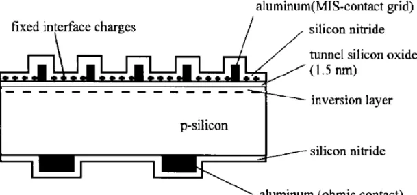
1.2.2 First-Generation MIS-IL Solar Cells
The cross-section of the first generation MIS-IL solar cell, including bifacial sensitivity, is shown in Fig 1.1. The inversion layer is induced by fixed positive charges present in the transparent insulator film[4-8], which covers both the silicon surface and the MIS contacts. In order to increased fixed charges in film, cell has to dip in cesium solution[10] and cesium ion cans easily be caught in the trap. Though cell degradation after cesium dip is faster, the following SiN layer can serve as a passivation layer and reduce the surface recombination[3,10]. In this structure, the ultrathin oxide layer (<2nm) blocks majority carrier (hole) currents injected into the metal at forward bias and reduces surface recombination. Therefore, a higher open circuit voltage of MIS solar cells than that of Schottky barrier solar cells can be achieved.
Fig 1.1: The cross-section of the first generation MIS-IL solar cell with bifacial sensitivity
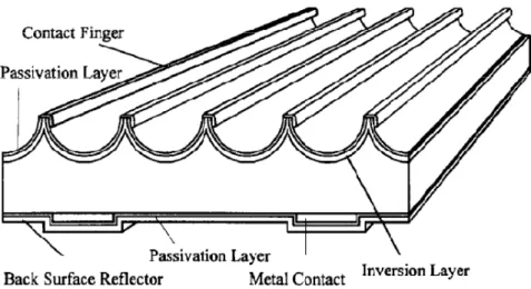
1.2.3 Second-Generation MIS-IL Solar Cells
The first-generation MIS-IL solar cells have a high conversion efficiency approach 20%, but the surface recombination velocity at the surface is still large due to low temperature PECVD SiN passavation[3,10]. From the simulation with PC-1D[3], the open circuit voltage can increase by 20-40mV with SiN deposition temperature increasing from 250 to 400 .℃ ℃ In second-generation MIS-IL solar cells, some treatments are done in order to further increase the efficiency as follows:
(a) Formation of special texture on semiconductor surface;
(b) Better surface passivation by high temperature deposited film before electrode deposition;
(c) Smaller contact area on the top of texture after removal of passivation layer.
Two types of second-generation MIS-IL solar cells are shown in Fig. 1.2 and Fig. 1.3
Fig. 1.2: Figure of a truncated-pyramid MIS-IL silicon solar cell
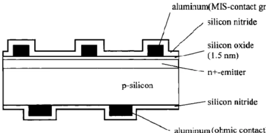
1.2.4 MIS-n
+p Solar Cells (MINP)
This kind of cells deposit Aluminum electrode on conventional diffused p-n junctions with thin tunneling oxide in between, resulting in hybrid MIS-n+p solar cells[3]. The MIS structure creates another junction to enhance the efficiency of p-n junction and surface recombination velocity can also be reduced by the thin tunneling oxide. Furthermore, with aluminum in substitution for silver electrode lowers the costs for mass production.
Fig 1.4: Schematic cross-section of the bifacial MIS-n+p solar cell (MINP)
1.3
MIS Stacked Solar Cells
Although the conversion efficiency of MIS solar cells can be compared with conventional diffused p-n junction cells, based on detail balanced limit, the upper limit of energy conversion efficiency of ideal photovoltaic devices with one energy band-gap is about 31.0%. That is to say, there is much more energy loss so far in this kind of
devices. To overcome this drawback, one of favorable high efficiency photovoltaic devices, stacked solar cells, has been demonstrated[11-13]. Stacked solar cells not only provide high energy conversion efficiency, but supply high open circuit voltage as well due to the electrically cascade of two current balanced solar cells. High voltage output lowers the ohmic losses at series resistance inside and outside the stacked cells. In addition, it makes possible the combination of photovoltaic-electrolysis system for hydrogen production with single cell in reality.
For an ideal stacked solar cell, all photo-generated carriers in the central sub-cells of the stacked solar cell can be efficiently recombined at the tunnel junctions. That is to say, current matching between sub-cells is an important issue to enhance the efficiency of stacked cells.
1.4
Motivation
In recent years, solar cells and fuel cells are seen as potential devices to overcome the problem of energy crisis. The combination of solar cells and fuel cell is an efficient way to construct a pollution-free energy providing system. Solar cells convert sun light to electricity during the day, and the remained electricity is converted into hydrogen by splitting water; fuel cells generate electricity from saved hydrogen at night.
voltage output is necessary, which can be achieved by stacked cells. Besides, to simplify the fabrication process and design consideration, MIS solar cell is a potential structure. Therefore, a series of experiment on MIS stacked solar cells have been done in this thesis.
1.5
About this work
In this work, three different junctions have been investigated, respectively. We use direct wafer bonding to achieve the tunneling diode with an n-type wafer and a p-type wafer. We also study the characteristics of MIS solar cells fabricated on n-type and p-type silicon wafer individually. Finally, we combine these two components to achieve a MIS stacked solar cell and study its photovoltaic properties.
Chapter 2
Principle of MIS solar cells
2.1
General Description of solar cells
For a solar cell, the current-voltage (I-V) characteristics in dark and under illumination are the most important method to evaluate a solar cell. While the cell is exposed to AM 1.5, only incident photons with energy larger than the energy bandgap Eg of active layer can be absorbed and generate electron-hole pairs. Electron-hole pairs
in depletion region or diffused into depletion region are separated by internal electric field and then collected by electrodes, afterwards.
In the dark, the current-voltage (I-V) characteristics of an ideal p-n junction solar cell which acts just like an ideal diode is given by
I = I e / − 1 (Eq. 2.1)
where IS referred to as the reverse saturation current of the diode, Va is the applied
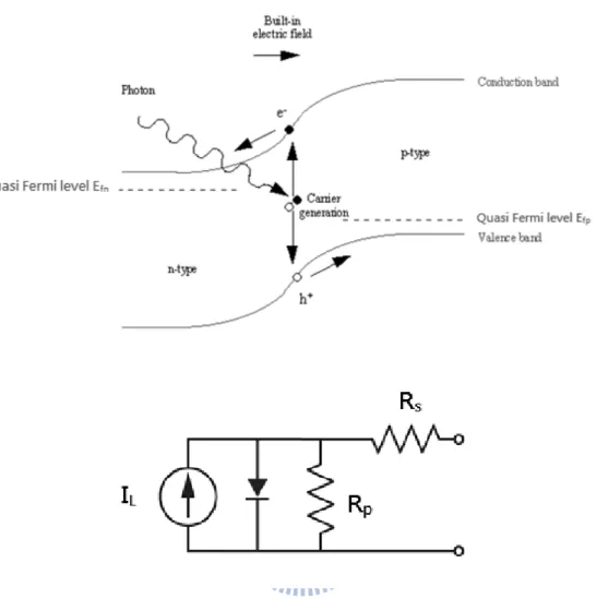
voltage, q = 1.6 ×10⁻¹⁹ C is the fundamental unit of charge, k = 1.38 ×10⁻²³ J/K is the Boltzmann's constant, and T is the absolute temperature. Fig 2.1 shows the energy-band diagram of a conventional p-n junction solar cell under solar illumination and the ideal equivalent circuit of the p-n junction solar cell under solar irradiation.
Fig 2.1: (a) band diagram of a conventional p-n junction solar cell under illumination (b) the ideal equivalent circuit of the p-n junction solar cell under solar irradiation
A light-generated current source IL parallel with the junction, and then the
current-voltage (I-V) curve simply shifted down. The behavior under illumination is represented by
I = I e / − 1 − I (Eq. 2.2)
and u volta is a w Fig 2 of qu load illum volta under illum Fig. 2.2: I Since a sol age and curr working po 2.2). Also, w uasi-Fermi l
resistance. minated cell age Vmax and
ination are I-V characte lar cell is a rent on a wo int correspo we identify levels in Fig . The shor l if the load d correspon shown in Fi eristics of a power sour orking poin onding to m
the open cir g 2.1(a) as t rt circuit c d resistance nding Imax. T FF = ig. 2.2. solar cell in
rce, the out nt of the illu maximum po rcuit voltag the voltage a current den is zero. Th Therefore, fi × × n the dark a tput power e uminated I-V ower output ge Voc which across the il nsity, ISC, i he maximu fill factor FF (Eq. 2.3)
and under ill
equals to th V curve. On t denoted a h is related lluminated is the curre m power is F can be exp lumination he product o n the curve, s Pmax (show to the separ cell with in ent through s obtained a pressed as of the there wn in ration nfinity h the at the
And the power conversion efficiency η which is defined as the ratio of the output electrical power to the incident optical power, is given by
η =Pm
Pin =
Vmax×Imax
Pin =
FF×Voc×Isc
Pin (Eq. 2.4)
From Eq. 2.4, to enhance the conversion efficiency, three important parameters, Voc, Isc and FF have to be put into consideration:
(a) For Isc enhancement, well designed collection fingers help the extract of photo
current and anti-reflection coating can improve the production of photo current. (b) For Voc enhancement, because Voc is related to the built-in potential of the
junction, material choosing is the first consideration. Furthermore, the recombination defects in junctions should be passivated not to reduce the Voc.
(c) Furthermore, the closer to unity FF is the better the conversion efficiency of a solar cell, while the fill factor FF corresponds to contact formation and carrier collection efficiency.
Air mass is the optical path length through Earth’s atmosphere for light from the sun. As it passes through the atmosphere, light is attenuated by scattering and absorption; the more atmosphere through which it passes, the greater the attenuation. For a thickness L0 of the atmosphere, the path length L through the atmosphere for solar
radiation incident at angle θ relative to the normal to the Earth's surface is L = L0 / cos θ.
radiation, is considered to have “air mass zero” (AM0). Similarly, the solar radiation after traveling through the atmosphere to sea level is referred to as AM1. However, the radiation angle of the sun changes with latitude and even from time to time. Consequently, AM1.5g, corresponding to a solar zenith angle of 48° and equals to 1000W/m2, is almost universally used to characterize solar cells at the Earth’s surface.
2.2
Transport Mechanism of MIS Junctions
In 1938, Walter H. Schottky suggested that a potential barrier could arise from a metal-semiconductor also diode known as Schottky diode. The current transportation for a Schottky diode is mainly due to majority carrier as opposed to minority carrier in p-n junction. The current density can be represented as
J = J e / − 1
where JS is the reverse saturation current density, q = 1.6 ×10⁻¹⁹ C is the
fundamental unit of charge, n is the ideality factor, k = 1.38 ×10⁻²³ J/K is the Boltzmann's constant, and T is the absolute temperature. The above equation is identical in the form to the equation of the p-n junction. However, the thermionic emission current is mainly due to majority carrier while p-n junction is due to minority carrier. Therefore, a smaller turn-on voltage can be expected in Schottky diode. For solar cell application, low turn-on voltage and the interface states of a Schottky diode will
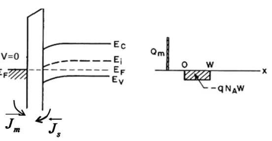
degrade cell performance, so a thin insulating layer is introduced into the interface. In the following paragraphs, seven regions of the J-V characteristics of an MIS solar cell with p-type semiconductor in dark and under illumination will be explained with Jm (current density flows from metal to semiconductor by thermionic emission), Js
(current density flows from semiconductor to metal by thermionic emission) and Je
(photo electron tunneling current density with help of traps).
(a) Dark — forward bias (negative bias at metal)
When the MIS diode is under forward bias, band near the junction bend upward. This band bending causes an accumulation of majority carriers (holes) near the oxide-semiconductor interface. For Schottky barrier diode, the thermionic emission current can easily pass through MS junction and result in high dark current. However, these carriers should pass the oxide with the assistance of traps existed in the oxide or tunneling for MIS junction with sufficient thin oxide. Therefore, exponential rising of the current with applied forward bias can be expected. As shown in Fig 2.3(a), the total current density
Fig (b) equil semi how issue g 2.3: (a) Ba Dark — ze When the librium. As shown conductor. to enlarge e. and diagram dark (b) ero bias MIS solar n in Fig 2 In MIS junc the depleti m and curren Charge dist cell is zer J = 2.4(a), a d ction, deple ion region b nt flow of a tribution at o biased, th = J − J = depletion r etion region by fixed ch a MIS solar accumulatio he net curr = 0 region form is always s harges in in cell under f on region rent is zero med near smaller than nsulator is a forward bias o due to the the surfac n p-n junctio a most impo s in ermal ce of on, so ortant
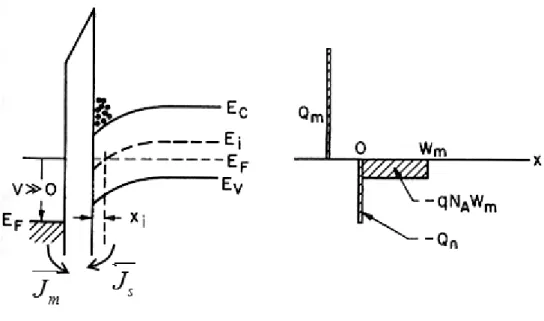
Fig 2 (c) D appe Unde reach 2.4 (a): Ban Dark — rev When the arance of i er this bias hes saturatio d diagram a Ch versed bias MIS solar inversion la condition, t on at large r and current harge distrib r cell is r ayer and re the total cur reverse bias J = J − flow of a M bution at de reverse bia educed ther rrent in cell s, as shown J ≅ −J ≅ MIS solar ce epletion regi sed, band rmionic emi l is determin in Fig 2.5(a ≅ const.
ell under zer ion bend down ission from ned by Jm co a) ro bias in da nward with m semicondu omponent w ark (b) h the uctor. which
Fig 2.5: (a) Band diagram and current flow of a MIS solar cell under reversed bias in dark (b) Charge distribution at inversion region
(d) Illuminated —large forward bias
When the MIS solar cell under illumination is forward biased, the Js and Jm flow as
same as that in dark. Besides, photo-generated electrons will flow into semiconductor along with the direction of electric field. The electrons in metal can also pass through the oxide under the assistance of the traps in the oxide. This current component is denoted as Je as shown in Fig 2.6. Under such condition, the total current is increased by Je and then total current density
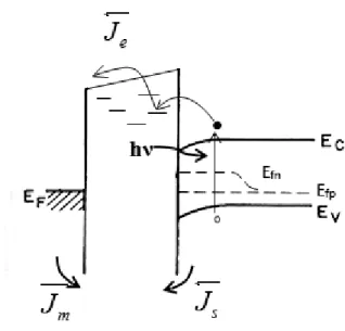
F (e) Il decre slope of th meta will c MIS ig 2.6: Band lluminated If the posi ease of elec e of band b he direction al emerge w cancel the n At this cas solar cell u d diagram a — zero cu itive bias v ctric field in bending cha of electric with the assis net thermion e, the bias under this co and current biased urrent (open voltage dec n the oxide. anges from p field, and t stance of ox nic emission J = voltage is c ondition. flow of a M under illum n circuit) creases, the As bias vo positive to then the ele xide traps. T n current an J − J − J called open MIS solar ce mination e Je compo oltage decre negative, c ectrons flow This current nd the total c = 0 circuit volt ell which is l onent decre eases to a ce correspondin wing from s t componen current den tage Voc. Fi large forwa eases due t ertain exten ng to the ch semiconduct nt, denoted sity ig 2.7 show ard o the nt, the hange tor to as Je, ws the
Fi (f) I curre photo show ig 2.7: Band Illuminated When the ents cancel e The only e o current an ws the energ d diagram a d — zero b MIS solar each other. existing cur nd this curre gy band diag and current f und bias (short c r cell is sh Therefore, t J = J − J rrent comp ent density gram under flow of a M der illumina circuit) hort circuit the current J − J = − onent that is also deno this conditi
MIS solar cel ation t connected J = −J can be dra oted as shor ion. ll which is o d, the therm
awn out fro rt current de open circuit mionic emi om the devi ensity Jsc. Fi ted ission ice is ig 2.8
Fig 2.8: Band diagram and current flow of a MIS solar cell which is zero biased under illumination
(g) Illuminated — reverse bias
When the MIS solar cell is under reverse bias, JS decrease due to the reduced thermionic emission probability. The total current
J = J − J − J = J − J
The current density Jm will reach saturation while if the intensity of the
illumination increases, Je increases. The energy band diagram under this condition is shown in Fig 2.9.
Fi
2.3
expe simp therm detai ig 2.9: BandFabri
In this sec riment. Dif plify the fabrmal evapora iled process (a) Wafer (b) Depos (c) Therm d diagram a
cation of
ction, we in fferent from rication pro ated through s is listed as rs cleaning w sit ultra-thin mal evaporat and current f undMIS Sola
ntroduce th m the high e ocess, electr h finger-typ follows: with traditio n oxide on w te electrode flow of a M der illuminaar Cells in
he fabricatio efficiency bi rodes and th pe metal ma onal RCA c wafers with s on the bacMIS solar cel ation
n this The
on process ifacial cell hin metal fil asks on ultra lean sputtering ck side of w ll which is resis
of MIS so discuss in 1 lms for carri a-thin insula wafers reverse bias olar cells in 1.2.2, in ord ier collectio ating layers sed n our der to on are s. Therespe (d) Annea (e) Therm oxide (f) Therm (g) Depos The struct ectively. Fig aling at 500 mal evapora mal evaporat sit a passiva ures of n-t g 2.10: Struc for 1hr i ℃ ate a thin la te front elec ation layer o type and p ctures of (a) n hydrogen ayer of met ctrodes on cells p-type MIS ) n-type sola n atmospher tal film via
S solar cel ar cell (b) p e a metal mas ls are show p-type solar sk on the t wn in Fig cell op of 2.10
Chapter 3
Properties of p-type MIS solar cells
In this chapter, we focus on the research on MIS solar cells with p-Si substrate. Different from conventional MIS solar cells, we deposit thin tunneling oxide with magnetic sputter instead of thermal oxide. The advantages of sputter oxide arethe film thickness and large tuning range of film quality. However, ion bombard effect will produce large amount of defect at the interface and in the oxide film, so some post annealing have to be done to passivate defects after oxide deposition
3.1
Photovoltaic Properties with Annealing Process
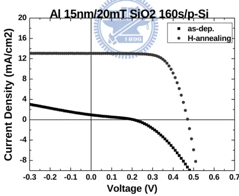
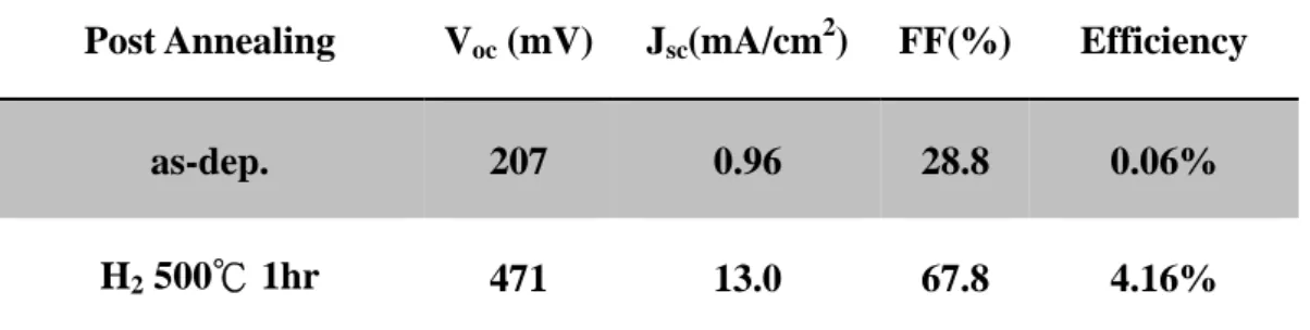
As show in Fig 3.1 and Table 3.1, cell with poor photovoltaic characteristic is obtained without post-oxidation annealing. From the J-V curve under AM1.5g irradiation, a low Voc and Jsc indicated that there is probably a great quantity of
recombination centers in the oxide film. According to the researches[14,15], high temperature post-oxidation annealing reduces the defect density in thin tunneling oxide and lowers leakage current in MIS diodes. In order to reduce the recombination centers in the tunneling oxide, a post-oxidation annealing is introduced in our fabrication process. In Fig3.1 and Table3.1, solar cells under illumination with annealing at 500℃ for 1hr in hydrogen atmosphere are shown. Because hydrogen can easily diffused into oxide film and can passivate Si dangling bonds by formation of Si-H bonds, samples
annealing at 500℃ in hydrogen atmosphere exhibit good photovoltaic properties with higher Voc, Jsc and FF (Table 3.1). From the capacitance-voltage (C-V) measurement
shown in Fig 3.2, with no post annealing, C-V curve have abnormal rapid drop at accumulation region, corresponding to large leakage current due to defects in ultra-thin oxide film with sputter. However, after high temperature H-annealing, the C-V curve only have small drop at accumulation region, indicating the suppression of recombination in oxide film, and an evidence of defect passivation is attain as same as which in J-V curve. -0.3 -0.2 -0.1 0.0 0.1 0.2 0.3 0.4 0.5 0.6 0.7 -8 -4 0 4 8 12 16 20
Curren
t Density (m
A/cm2)
Voltage (V) as-dep. H-annealingAl 15nm/20mT SiO2 160s/p-Si
Post Annealing Voc (mV) Jsc(mA/cm2) FF(%) Efficiency
as-dep. 207 0.96 28.8 0.06%
H2 500℃ 1hr 471 13.0 67.8 4.16%
Table 3.1: Photovoltaic properties of cells with and without H-annealing
-3 -2 -1 0 1 2 3 0.0 0.2 0.4 0.6 0.8 1.0
Al 15nm/20mT SiO2 160s/p-Si
C/Cmax
Voltage (V)
as-dep. H-annealingFig 3.2: C-V measurement of cells with and without H-annealing
3.2
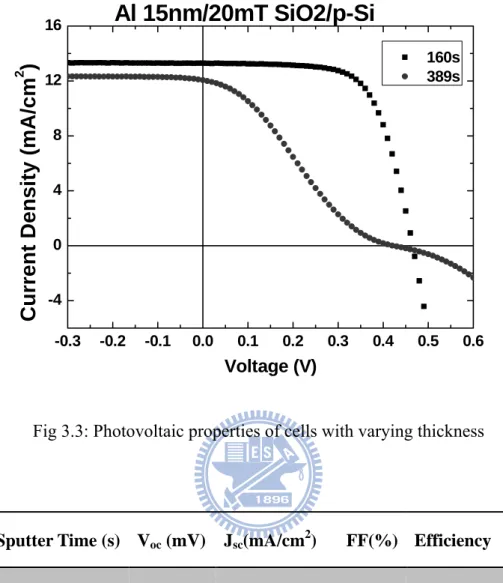
Photovoltaic Properties with Different Oxide Thickness
In order to increase the Voc, a thin tunneling insulating layer is a must for MIS
solar cells. Once the insulator is too thick, the tunneling probability reduce significantly, and then photo carriers cannot be collected by electrodes. According to the simulation
thicker than 2nm and cells show no photovoltaic properties[16]. Therefore, the oxide thickness for the performance of MIS solar cell is critical. With the increasing oxide thickness, the voltage drop on insulator increases, and hence decrease the electric field at the surface of semiconductor. Moreover, a thicker oxide will also lower the tunneling probability of minority carriers, so the drop of current in the J-V curve starts from forward bias.
From Fig 3.3 and Table 3.2, we can also see the tendency of fill factor decreasing while thickness becomes thicker. The J-V curve of sample with sputtered 389s drop at small forward bias, confirmed with above discussion. Although Jsc with sample of
sputtered oxide 389s is nearly no change due toslightly decreasing in electric field and tunneling probability at zero bias, low fill factor decreases cell efficiency dramatically and a further decrease with thicker oxide is expected.
-0.3 -0.2 -0.1 0.0 0.1 0.2 0.3 0.4 0.5 0.6 -4 0 4 8 12 16
Cur
rent Density (m
A/cm
2)
Al 15nm/20mT SiO2/p-Si
Voltage (V) 160s 389sFig 3.3: Photovoltaic properties of cells with varying thickness
Sputter Time (s) Voc (mV) Jsc(mA/cm2) FF(%) Efficiency
160 463 12.5 71.9 4.18%
389 422 12.1 26.2 1.34%
Table 3.2: Photovoltaic properties of cells with varying thickness
3.3
Photovoltaic Properties with Different Working Pressure
Since we use magnetic sputter to deposit the tunneling oxide on cells, several parameters can be tuned to change the film quality like gas flow rate, working pressure,
out how the film quality changed with different working pressure.
As shown in Fig 3.4 and Table 3.3, the best Voc reaches 475mV at the working
pressure 20mT. As working pressure increases, the Voc decreases to 350mV at working
pressure 40mT. From C-V measurement shown in Fig. 3.5, a curve shift toward zero with the increasing working pressure reveals the reduced barrier height at MIS junction. Furthermore, the small rising at point A indicates defects which are induced by increasing ion bombards probability in oxide film. Therefore, smaller Voc are obtained
because of lower barrier height and lager defect density with the increasing working pressure. -0.1 0.0 0.1 0.2 0.3 0.4 0.5 0.6 -10 -5 0 5 10 15 20
Al 10nm/ SiO2 /p-Si
Current Densi ty (mA/ cm 2 ) Voltage (V) 20mT 30mT 40mTPressure (mTorr) Voc (mV) Jsc(mA/cm2) FF(%) Efficiency
20 475 16.8 64.3 5.15%
30 386 16.3 68.3 4.31%
40 350 14.8 66.8 3.45%
Table 3.3: Photovoltaic properties of cells with varying working pressure
-3 -2 -1 0 1 2 3 0.0 0.2 0.4 0.6 0.8 1.0
Al 10nm/ SiO2 /p-Si
C/C
ma x Voltage (V) 20mT 30mT 40mTFig 3.5: C-V measurement of cells with varying working pressure
3.4
Photovoltaic Properties with Different Metal Thickness
In our MIS solar cells, due to fabrication simplicity, metal electrodes are thermal A
collection efficiency, as shown in Fig 3.6 and Table 3.4 with no thin metal film. To overcome this problem, a thin metal film for carrier collection is introduced into our cells. Although a thick metal film has good carrier collection efficiency, the reflection is also increase with the increasing metal thickness. Hence, the tradeoff between transparent and carrier collection efficiency is important.
In our work, with decreasing metal film from 15nm to 10nm, an apparent enhancement of Jsc from 13 to 16 mA/cm2 is shown in Fig 3.5 and Table 3.4.
-0.1 0.0 0.1 0.2 0.3 0.4 0.5 0.6 -8 -4 0 4 8 12 16
20
Al/20mT SiO2 160s/p-Si
Current Density (mA/cm
2 )
Voltage (V)
Al 15nm Al 10nm No metal
Metal Thickness (nm) Voc (mV) Jsc (mA/cm2) FF(%) Efficiency
No metal 411 0.44 64.8 0.12%
10 475 16.9 64.3 5.15%
15 463 12.5 71.9 4.18%
Table 3.4: Photovoltaic properties of cells with varying thickness of Al film
3.5
Summary
In this chapter, works on MIS solar cells with p-Si have been discussed at different cases. From the data shown above, post-oxidation annealing in hydrogen atmosphere is a must for cells with sputter oxide due to the high defect density in film. Although film quality can be modified by post annealing, the thickness and sputtering working pressure are also key factors in MIS solar cells, and the best case is sputtered 160s with RF power 50W and working pressure 20mTorr. Finally, we change the thin collecting metal thickness and analyze its properties; cells with aluminum thickness 10nm in our structure have highest efficiency. Although there is only a slightly enhancement in Voc
with decreasing metal thickness from 15nm to 10nm, higher efficiency because of higher Jsc do help the performance of MIS stacked solar cells.
solar high meta 5.1eV dopin Ther Fig
Chapte
In this chap r cells, thin Voc by for al should be V. However ng density refore, a sma g 4.1Metal-er 4
P
pter, n-type tunneling o rming a MI e used on n r, the barrie is 1016 cm-3 all Voc coul -SemiconduPropert
MIS solar oxide are d IS junction n-Si, so we er height di 3 as shown ld be expect uctor work fties of n
cells are dis deposited by n with large choose gold ifference be in Fig 4.1, ted. function dif
n-type M
scussed. As y magnetic e barrier he d which ha etween Au , lower than fference verMIS sola
s same as th sputter. In eight, a high as high work and n-Si is n that betwe rsus dopingar cells
hat in p-type order to ac h work fun k function s only 0.6V een Al and (From Sze[ e MIS chieve nction about V with p-Si. [17])4.1
Photovoltaic Properties with Annealing Process
In p-type MIS solar cells, post-oxidation annealing is necessary to get good photovoltaic characteristics (Fig 3.1 and Table 3.1), so the same annealing process annealing at 500 for 1hr in hydrogen atmosphere is also done. Better photovo℃ ltaic characteristics as shown in Fig4.2 after H-annealing are obtained without doubt. Different from p-type MIS solar cells, the cell with no treatment has a not bad fill factor 50.7%, still lower than that with H-annealing though. With C-V analysis (Fig.4.3), the curve drop of as-dep. sample at accumulation region is not as much as that of p-type sample, so n-type MIS solar cells without annealing have better photovoltaic properties. After H-annealing process, though the curve still has a small drop at accumulation region, the right shifted curve indicates the rise of barrier height due to passivation by the formation of Si-H bonds, and then the Voc after H-annealing increases from 313mV
to 422mV. However, this value is still lower than that of p-type cells because of the smaller barrier height mentioned in the beginning of chapter4.
-0.3 -0.2 -0.1 0.0 0.1 0.2 0.3 0.4 0.5 -4 0 4 8 12 16
Au 20nm/20mT SiO2 389s/n-Si
Current Density (m
A/cm
2)
Voltage (V) as-dep. H-annealingFig 4.2: Photovoltaic properties of cells with and without H-annealing
Post Annealing Voc (mV) Jsc(mA/cm2) FF(%) Efficiency
as-dep. 313 13.4 50.7 2.13%
H2 500℃ 1hr 422 14.4 58.4 3.55%
-3 -2 -1 0 1 2 3 0.0 0.2 0.4 0.6 0.8 1.0
Au 20nm/20mT SiO2 389s/n-Si
C/
C
ma x Voltage (V) As-dep. H-annealingFig 4.3: C-V measurement of cells with and without H-annealing
4.2
Photovoltaic Properties with Different Oxide Thickness
As discussed in section 3.2, insulating thickness is critical for cell efficiency. We change the sputter time to control the same film thickness as what we do on p-type cells. As shown in Fig4.4 and Table4.2, the tendency from 389s to 778s exhibit lowering tunneling probability and a large voltage drop on thick oxide. The increase in Voc from
160s to 389s can be explained by the increasing Schottky barrier height with the increasing oxide thickness[18-20] and better interface defect passivation.
The best tunneling oxide thickness of n-type MIS solar cells is sputtered 389s (Fig4.4 and Table4.2), thicker than that of p-type in our work. Try to explain this huge
difference with the transport mechanism, in p-type MIS solar cells under illumination, the majority carrier holes are easily blocked by thin oxide due to lower diffusion constant in Si and minority carrier electrons are tunneling through oxide film to produce light current. On the contrary, in n-type MIS solar cells, majority carriers are electrons which are more difficult to be blocked with higher diffusion constant. Therefore, a thicker oxide is needed in MIS solar cells on n-Si.
-0.2 -0.1 0.0 0.1 0.2 0.3 0.4 0.5 0.6 -4 0 4 8 12 16
Au 20nm/20mT SiO2/n-Si
Current density (m
A/cm
2)
VA (V) 160s 389s 583s 778sSputter Time (s) Voc (mV) Jsc(mA/cm2) FF(%) Efficiency
160 295 14.0 54.7 2.25%
389 366 13.4 56.4 2.76%
583 346 11.6 35.9 1.44%
778 320 11.1 22.3 0.80%
Table 4.2: Photovoltaic properties of cells with varying thickness
4.3
Photovoltaic Properties with Different Working Pressure
In Fig. 4.5 and Table 4.3, the tendency of Voc of n-type cells with increasing
working pressure is the same as that of p-type. However, in Fig. 4.6, the C-V curves shift is not apparent between 30mT and 40mT, indicating almost the same barrier heights and Voc. However, cells with working pressure 20mT show no rising at point A
and steep slope in transition from inversion to accumulation, demonstrating lower defect density in oxide film and interface. Therefore, the Voc of n-type cells with
working pressure 20mT reach 422mV, which is the best value in our work, greatly larger than cells with 30mT and 40mT.
-0.1 0.0 0.1 0.2 0.3 0.4 0.5 -4 0 4 8 12 16 20
Au 20nm/SiO2/n-Si
Current Densi ty (mA/ cm 2 ) Voltage (V) 20mT 30mT 40mTFig 4.5: Photovoltaic properties of cells with varying working pressure
Pressure (mTorr) Voc (mV) Jsc(mA/cm2) FF(%) Efficiency
20 422 14.4 58.4 3.55%
30 339 14.7 55.5 2.77%
40 313 14.2 59.9 2.66%
-3 -2 -1 0 1 2 3 0.0 0.2 0.4 0.6 0.8 1.0
Au 20nm/SiO2/n-Si
C/C ma x Voltage (V) 20mT 30mT 40mTFig 4.6: C-V measurement of cells with varying working pressure
4.4
Photovoltaic Properties with Different Metal Thickness
As discussed in section 3.4, the thickness of metal film is a tradeoff between collection efficiency and reflection. In n-type cells, we use gold as front electrode to form MIS junctions. Since the reflection of gold is different from aluminum, the optimum thickness is also different. As shown in Fig 4.7 and Table 4.4, Jsc reaches about
14.3mA/cm2 with 15nm gold film, and keeps no change while increasing to 20nm. Therefore, an optimum thickness between 15nm and 20nm of gold film on n-type MIS solar cells can be expected. However, there is 40mV difference between 15nm and 20nm, which is not present in p-type solar cells (Fig 3.6 and Table 3.4). This phenomena
result from the nickel deposited on the gold film, which lowers the work function of gold while gold is thinner than 20nm. Since the barrier height is lowered by the lower work function, the Voc is reduced.
-0.1 0.0 0.1 0.2 0.3 0.4 0.5 -4 0 4 8 12 16
20
Au/20mT SiO2 389s/n-Si
Current Densi ty (mA/ cm 2 ) Voltage (V) 20nm 15nm 10nm 5nm
Fig 4.7: Photovoltaic properties of cells with varying thickness of Au film
Metal Thickness (nm) Voc (mV) Jsc (mA/cm2) FF(%) Efficiency
5 196 0.91 36.6 0.07%
10 329 7.17 40.7 0.96%
15 381 14.3 54.0 2.95%
4.5
Summary
In this chapter, n-type MIS solar cells are realized and analyzed with different parameters. The best tunneling oxide thickness is sputtered 389s with working pressure 20mTorr, thicker than that of p-type cells, and this phenomena can be explain with transport mechanism discussed in section 2.2.
As same as the tendency with the change of annealing process, oxide thickness, metal thickness and working pressure, we get the optimum fabrication parameters and achieve the Voc 422mV.
Chapter 5
Experiments of MIS Stacked Solar Cells
5.1
Tunneling Diode
5.1.1 General Description
Tunneling diode also referred as Esaki diode[21-23], is one of the most important issues affecting stacked solar cell performance. The problem of tunnel junction formation is related to the demand of obtaining uniformly highly doped layer without defects which result in carrier recombination and leakage current in depletion regions. In a common tunneling diode, degenerate semiconductors[17,24] are used to increase tunneling probability through depletion region.
E − E = kT ln (Eq. 5.1) E − E = kT ln (Eq. 5.2)
Where Nc and Nv are referred to as effective density of states, n0 and p0 are doping
density. From Eq. 5.1 and Eq. 5.2, degenerate semiconductor can obtain with n0 and p0
lager than Nc and Nv.
The current-voltage properties of a tunneling diode is shown in Fig 5.1, different from conventional p-n junction, the I-V curve is ohmic at small voltage while negative differential resistance (NDR) appears with increasing forward bias. The current-voltage characteristic of a tunneling diode can be explained using the band diagram and J-V characteristic shown schematically in Fig 5.1. When a reverse bias is applied, Fig 5.1(a),
current flows by electron tunneling from occupied states on the p-side valence band into unoccupied states in the n-side conduction band. In equilibrium, with no applied bias, shown in Fig 5.1(b), the net tunneling current is zero. With a small forward bias, current flow by electron tunneling gives rise to a peak current Ip at voltage Vp, as labeled in Fig
5.1(c). When the conduction band minimum on the n side is raised above the valence band maximum on the p side, the valley current Iv results at a voltage Vv in Fig 5.1(d).
With further increase in the voltage, the current increases due to tunneling through defect states in the depletion layer and thermionic emission over the diode internal barrier, Fig 5.1(e).
Fig 5.1: Schematic energy band diagram and current-voltage property of tunneling diode with varying bias (From Y. Yan[25])
In a tunneling diode, the doping profile is key point for the performance[25-27]. Once an abrupt doping profile is obtained, the resistance at the junction is decreased. In other words, less voltage loss in a stacked solar cell with a higher Voc could be achieved. On
the contrary, the broadening of the abrupt doping profiles increases the tunneling diode depletion region and significantly reduces the tunneling probability through depletion region. Consequently, stacked solar cell performance will dramatically be degraded.
With ion implantation, a common way to achieve tunneling diode, the doping profile of junction is hard to control. Therefore, we use direct wafer bonding to realize a good tunneling junction between two MIS solar cells.
5.1.2 Bonding Theorem
Direct wafer bonding generally refers to a process which two cleaned wafers adhere to each other without intermediate medium. If two polished wafers are brought into close sufficiently, attractive forces could pull the two bodies together into intimate contact so that bonds can form across the interface. Nevertheless, the bonding force is too weak that wafer would debond during suffering a small shear force. To strengthen the bonds across the interface, the room temperature bonded wafers have to undergo a high temperature annealing, and then two wafers can adhere to each other permanent.
hydrogen bonds or strong chemical bonds of metallic, ionic or covalent may mediate the adhesion. At room temperature, the attraction between two contacted cleaned wafers is seen as a van der Waals forces or hydrogen bonds[28]. After the subsequent heat treatment, the chemical bonds will be formed gradually at the interface, increasing the bonding energy.
The bonding energy is determined by substrate, annealing temperature, surface cleaning, and surface treatments and so on. Among these process parameters, surface cleaning is the most important. In the research, a particle with diameter 0.5um makes diameter 2.5 mm unbounded areas, so wafer cleaning in clean-room before bonding is a better way to enhance the yield and bonding quality. In reality, the bonding strength and electrical properties can even close to a bulk material with carful cleaning process and high temperature annealing.
5.1.3 Fabrication of Tunneling Diodes
The fabrication processes of a tunneling diode by direct wafer bonding are listed as follows
(1) Wafer are cleaned with RCA clean (2) Ion implantation at the polished side
(3) Dopants activated with rapid thermal annealing (RTA) 1050 30s℃ (4) Furnace 600 30 min in N2 to reco℃ very implantation damage
5.1
show (5) Wafer (6) Ultras (7) Direct and then Pu (8) Heate (9) Al 100 contacts an Fi1.4 Resul
The curren wn in Fig 5 r are dipped sonic cleanin t bond n-typ ut the bonde d up to 500 0nm and Ni nd measure ig 5.2: Schet and Dis
nt-voltage c .3. Without d in diluted H ng with ace pe and p-typ ed samples for 1 hou ℃ i 100nm are its J-V prop ematic top vcussion
characteristi t furnace at HF to remov etone and IP pe Si wafer into a clam ur e deposited pertiesview and sid
ics of tunne t 600℃ for ve native ox PA, respectiv rs with polis mp (Fig 5.2) on n-type a de view of b eling diode r 30 minute xide vely shed sides e and p-type S bonding clam fabricated es to recove each other in Si to form o mp by bondin ery implant n IPA ohmic ng are tation
damage, the lower current is attained without doubt. Moreover, the forward bias current is lower than reversed bias current. After furnace annealing, current raises at least two orders at reversed bias and about four orders at forward bias (Fig 5.3), and J-V curves shows no NDR in tunneling diode but a typical characteristic of a diode with large reversed saturation current.
-1.2 -0.8 -0.4 0.0 0.4 0.8 1.2 1E-6 1E-5 1E-4 1E-3 0.01 0.1 1
Curre
nt De
ns
ity
(A/c
m2
)
Foward Bias (V) RTA RTA+FurnaceJ-V Properties of Bonding Junction
Fig 5.3: Current-Voltage properties of bonded samples in dark with and without furnace annealing
To explain these strange J-V properties, we measure the junctions between ion implantation regions and wafers. From Fig 5.4, we can conclude that without furnace annealing, the junctions between ion implantation regions and wafers, corresponding to
n-n+ and p-p+ internal junctions, dominate the J-V properties and exhibit the opposite trend. With Furnace annealing, junctions vanished due to dopants diffusion and an ohmic curve with large current density are obtained because of defects diminishing.
-1.2 -0.8 -0.4 0.0 0.4 0.8 1.2 1E-7 1E-6 1E-5 1E-4 1E-3 0.01 0.1
Current Density (A/cm
2 )
Forward Bias (V)
RTA
RTA+Furnace
Fig 5.4: Current-Voltage properties of single wafer under dark with and without furnace annealing
Although the bonded sample shows no NDR in J-V curve (Fig 5.3), indicating insufficient doping activation or defects in the central junction, the current density reaches 10mA/cm2 with 20mV voltage drop, which would only slightly degrade the performance of MIS stacked solar cells. Therefore, we use this junction as the central
junction for MIS stacked solar cells.
5.2
Fabrication of MIS Stacked Solar Cells
To realize a MIS stacked solar cell, we should integrate three different junctions discussed early together. Starting from a bonded sample first, n-type and p-type MIS junctions are fabricated on both sides. However, 4-inch Si wafers has a thickness about 525um, which is thicker than the skin depth of visible light, so the cell on the back side under illumination can absorb light hardly. From point of current matching, net current output would be limited by bottom cell which generates less current. Consequently, a thinning process of bonded sample has to be done before two MIS junction fabrication to increase current in stacked cells. Although bonded sample can suffer mechanical thinning process, huge amount of defects at the surface are produced simultaneously. Hence, additional chemical etching process is introduced to remove surface defect and thin the wafer at the same time. The fabrication processes of MIS stacked solar cell are listed below:
(1) Bonded samples thinning with sand paper
(2) Dip samples into Si etchant (HF:CH3COOH:HNO3=6:7:20) to remove surface
defects and thin the samples at the same time
F
5.3
As d we d time. the t insuf diffic (4) H-ann (5) The to (6) The bo (7) The st Fig 5.5: StruResul
In this sect discussed ab dip cells into. However, top reveals fficient pass culty to mai nealing 500℃ op cell depo ottom cell d tructures of uctures of M
ts and Di
tion, we sho bove, thinni o Si etchant as shown i a low leak sivation and intain the qu 1hr to pa ℃osit the trans deposit rear f MIS stacke MIS stacked
scussions
ow the J-V ng process t to remove in Fig 5.6, o kage current d high defe uality of sta assivate defe sparent stru electrode ed solar cell d solar cell ws of MIS S
characterist is essential damaged l only the sta t. The leaka ect density. acked cells. fects in oxid ucture as sam ls are shownwith top cel
Stacked S
tics in dark l to enhance ayer and th acked cell w age current Therefore, de film me as that in n in Fig 5.5 l is (a) n-typolar Cells
and under e cell efficie hin the thickwith p-type ts of others fabrication n section 2.3 pe (b) p-typ
s
solar irradia ency. Afterw kness at the cell thinnin are high d n uncertainty 3 pe ation. ward, same ng on due to y is a-1.2 -0.8 -0.4 0.0 0.4 0.8 1.2 1E-6 1E-5 1E-4 1E-3 0.01 0.1 1 10
100
MIS Stacked Solar Cells (Dark)
no thinning n-thinning p-thinning
Current Density (mA
/cm
2 )
Forward Bias (V)
Fig 5.6: Current-voltage properties of MIS stacked solar cells in dark with (a) no thinning process (b) n-type cell thinning on the top (c) p-type cell thinning on the top
The current-voltage characteristics of MIS stacked solar cells under AM1.5g are shown in Fig 5.7 and Table 5.1. The cell without thinning process exhibits low Jsc
5.25mA/cm2 because the current is limited by bottom cell discussed in section 5.2. After thinning the top n-type cell to 50nm approximately, a much higher Jsc 16.5mA/cm2 is
obtained. However, the large leakage current suppresses the photovoltaic performance and the cell with n-type thinning on the top reaches the Voc 414mV.
Since the cell with p-type thinning on the top reveals a low leakage current, the Voc
junction MIS solar cells discussed in Ch3 and Ch4, demonstrating the utility of stacked cells. In this structure, the bottom cell is n-type MIS solar cells; the photo current of n-type cells are determined by minority carriers, holes, which have a lower mobility and cannot be collected by electrodes as easily as electrons. Hence, better photovoltaic properties of cells with n-type thinning on the top can be expected.
-0.1 0.0 0.1 0.2 0.3 0.4 0.5 0.6 0.7 0.8 -4 0 4 8 12 16
20
MIS Stacked Solar Cells (illumination)
Current Densi ty (mA/ cm 2 ) Voltage (V)
n-type on the top without thinning n-type thinning on the top
p-type thinning on the top
Fig 5.7: Current-voltage properties of MIS stacked solar cells under illumination
Cell Voc (mV) Jsc (mA/cm2) FF(%) Efficiency
No thinning 437 5.25 23.6 0.54%
n-thinning 414 16.5 25.2 1.71%
5.4
Summary
In this chapter, tunneling diode fabrication using direct wafer bonding is realized first. Although the bonded samples show no NDR which should present in tunneling diode, high reversed saturation current diodes are achieved with only 40mV loss while current density reach 10mA/cm2. Finally, we integrate n-type and p-type MIS solar cells on bonded sample to realize MIS stacked structure. The Voc of MIS stacked cells reach
593mV, lager than that of p-type and n-type cells, demonstrating that the structure is practical and have its potential to achieve water splitting.
Chapter 6
Conclusion and Future Work
6.1
Conclusion
In this thesis, MIS stacked solar cells are introduced and achieved in order to reach high voltage output.
First, we give general description of the transport mechanism of MIS solar cells in Chapter2. We also study the MIS solar cells on n-type and p-type of substrates in chapter3 and chapter4. The influence of fabrication parameters such as annealing process, tunneling oxide thickness, working pressure and metal thickness on MIS solar cells are investigate. With the best conditions, we get the Voc equals to 475mV on p-type
cells and 422mV on n-type cells.
In the beginning of chapter5, we introduce the fabrication of tunneling diode by direct wafer bonding. Although the bonded samples exhibit no NDR at small forward bias, diodes with high reversed saturation current are accomplished and can be used in the MIS stacked solar cells. Afterwards, MIS stacked solar cells are realized by integrating two types of MIS solar cells on bonded samples and best Voc equals to
593mV in our experiment is obtained.
6.2
Future Work
are still many issues to be investigated. First, the voltage drop at the central junction could be lowered by further improving the tunneling current with proper doping activation and defect passivation. Moreover, the thickness of upper cells and bottom cells in stacked cells should be precisely controlled and the current matching could be achieved.
Afterward, in order to enhance the efficiency, Jsc is the important issue to be
improved. Surface texturing by chemical etching is a common way to reduce surface reflection while some researches indicate that Voc would slightly decrease. Besides,
transparent conductive oxide such as ITO and ZnO can be introduced in our structure with the aid of sputter to further increase Jsc[29].
Finally, though the combination between solar cells and fuel cells is still a big challenge, our research does help the development of solar cells and the living of human beings.
Reference
[1] Zhores I. Alferov, V. M. Andreev, M. B. Kagan, I. I. Protasov,and V. G. Trofim,
Fiz. Tekh. Poluprovodn ,Vol.4 ,pp.2378 (1970)
[2] Zhores I. Alferov ,Rev. Mod. Phys. Vol.73, pp.767 - 782 (2001) [3] R. Hezel, Prog. PV Res. Appl. ,Vol.5, pp.109 (1997)
[4] R. Hezel, Solid State Electron., Vol.24, pp.863 (1981)
[5] R. Hezel and R. Schorner, J. Appl. Phys., Vol.52, pp.3076 (1981).
[6] R. Schorner and R. Hezel, IEEE Trans. Electron. Devices, ED-28, pp.1466 (1981) [7] R. Hezel, Conf. Rec. 16th IEEE Photovoltaic Specialists Conf., San Diego,
pp.1237 (1982)
[8] K. Jaeger and R. Hezel, IEEE Trans. Electron. Devices, ED-32, pp.1824 (1985) [9] R. Hezel, W. Hoffmann and K. Jaeger, Proc. 10th European Photovoltaic Solar
Energy Conf., Lisbon, pp. 511 (1991)
[10] A Metz, R Meyer, B Kuhlmann, M Grauvogl, R. Hezel, 26th PVSC; Sept. 30-Oct. 3,1997; Anaheim, CA, pp.31
[11] T Takamoto, E Ikeda, H Kurita, M Ohmori, Applied Physics Letters, Vol.70, pp.381 (1997)
[12] K. A. Bertness, Sarah R. Kurtz, D. J. Friedman, A. E. Kibbler, C. Kramer, and J. M. Olson, Appl. Phys. Lett. Vol.65, pp.989 (1994)
[13] Arvind Shah, J. Meier, E. Vallat-Sauvain, C. Droz, U. Kroll, N. Wyrsch, J. Guillet and U. Graf, Thin Solid Films, 403 –404, pp.179–187 (2002)
[14] K. Fukuda, W. J. Cho, K. Arai, S. Suzuki, J. Senzaki, and T. Tanaka, Appl. Phys. Lett., Vol.77, pp.866 (2000)
[15] YL Liu, O Maida, M Takahashi, H Kobayashi, J. Electrochem. Soc., Volume 151, Issue 12, pp. G824-G828 (2004)
[16] MAG El-Sayeda, S Abdel-Rady, Desalination, Vol.209, pp.15-22 (2007)
[17] S. M. Sze, “Physics of Semiconductor Devices” 2nd Ed. (Wiley, New York, 1981) [18] WA Anderson, JK Kim, AE Delahoy, IEEE Transactions on Electron Devices, Vol.
ED-24, pp.453-457 (1977)
[19] KK Ng, HC Card, IEEE Transactions on Electron Devices, Vol. ED-27, pp.716-724 (1980)
[20] J. P. Ponpon and P. Siffert, J. Appl. Phys. Vol.47, pp.3248 (1976) [21] L. Esaki, Phys. Rev., Vol.109, pp.603 (1958)
[22] L. Esaki, Proc. IEEE, Vol.62, pp.825 (1974)
[23] L. Esaki, IEEE Transactions on Electron Devices, Vol. ED-23, pp.644 (1976) [24] DA Neamen, “Semiconductor Physics and Devices” 3rd Ed. (McGraw-Hill, New
York,2003)
[26] R Stengl, KY Ahn, T Mii, WS Yang, U Gösele, Jpn. J. Appl. Phys., Vol.28, pp. 2405-2412 (1989)
[27] R. H. Esser, K. D. Hobart, and F. J. Kub, J. Electrochem. Soc., Vol. 151, pp.G387-G390 (2004)
[28] QY Tong, U Gösele, “Semiconductor wafer bonding :science and technology” [29] J Shewchun, D Burk, MB Spitzer - IEEE Transactions on Electron Devices, Vol.27,
Vita
Hsin-Yu Lee was born at 25, Aug. 1986 in Tainan, Taiwan. He
received the B.S. degree in Department of Electrical Engineering, National Taiwan University, Taipei, Taiwan in 2007. The M.S. degree will receive in Department of Photonics, National Chiao Tung University, Hsinchu, Taiwan in 2009. His research include the analysis and fabrication of MIS stacked solar cells.
Publications:
[1] Hsin-Yu Lee, Yi-Shian Max Lin, Kuang-Yang Kuo, Tzu-Yueh Chang, and Po-Tsung Lee, “Post-annealing Temperature Effect on the Optical and Electrical Properties of the Nano-structured Si/SiO2 Multilayer”, ISSCT’08, Taipei, Taiwan