適用於IEEE802.11a接收機之差異積分調變CMOS頻率合成器設計
102
0
0
全文
(2) CMOS Delta-Sigma Frequency Synthesizer Design for 802.11a Transceiver. 適用於 IEEE802.11a 接收機之差異積分調變 CMOS 頻率合成器設計. 研 究 生:李維傑. Student:Wei-Jie Lee. 指導教授:溫瓌岸. Advisor:Dr. Kuei-Ann Wen. 國 立 交 通 大 學 電機資訊學院 電子與光電學程 碩 士 論 文 A Thesis Submitted to Degree Program of Electrical Engineering Computer Science College of Electrical Engineering and Computer Science National Chiao Tung University in Partial Fulfillment of the Requirements for the Degree of Master of Science in Electronics and Electro-Optical Engineering June 2004 Hsinchu, Taiwan, Republic of China. ii.
(3) 適用於 IEEE802.11a 接收機之差異積分調變 CMOS 頻率合成器設計. 研 究 生:李維傑. 指導教授:溫瓌岸 教授 國立交通大學. 電機資訊學院 電子與光電學程﹙研究所﹚碩士班. 摘. 要. 本篇論文主旨在於設計可工作於 1.8V 直流電壓且以全積體化互補式金半導體 0.18-um 為製程,適用於 IEEE802.11a 接收機之差異積分調變分數型頻率合成 器。此頻率合成器在 5.12GHz~5.376GHz 之頻率合成範圍內可以提供 16Hz 之頻率解 析度,並且具有 6us 之快速鎖頻與低分數突波的特性。所設計的頻率合成器電路包 含壓控震盪器(Voltage Controlled Oscillator)、相位/頻頻比較器(Phase-Frequency Detector)、多模數除頻器(multi-modulus divider)、電荷充放電濾波器(Charge-Pump filter)以及三階之差異積分調變器。 電壓控制振盪器由負電阻,螺旋型電感和 P/N 接面可變電容所組成,振盪器 的輸出頻率可經由可變電容調整,經設計於控制電壓 1.8V 內,振盪器輸出頻率 範圍可從 4.88GHz 到 5.436GHz。. iii.
(4) 在前置除頻器(prescaler)方面,為了能達到在高速操作並且低耗電的目標, 故採用 pseudo-NMOS 搭配 TSPC 型式的除法器來完成。至於多模數除頻器,可 除頻倍數從 16 到 31。整個除頻器經測量最高可工作在 5.9GHz。相位/頻率偵測 器是比較外部輸入參考信號與內部除頻後信號的相位/頻率差,產生充電 UP 和放 電 DN 的數位信號,此數位信號會透過電荷充放電轉成類比訊號,透過三階低通 濾波器變成近似 dc 的類比連續信號以控制壓控震盪器。 除以上所述電路之外,此頻率合成器亦整合一個全數位管線化,以多級雜訊 整形為架構之三階差異積分調變器,藉由此差異積分調變器的雜訊整形技術來降 低由除數控制訊號所產生的相位雜訊,此差異積分調變器製作於可編程邏輯程式 元件(FPGA)。經測量此差異積分調變器能達到 60dB 雜訊整形的能力,此外對調 變器輸出取樣 218 筆資料平均後,其分數的產生精確度可達到 99.999%。 此頻率合成器使用是採用 UMC 0.18um CMOS 1P6M 製程並操作在 1.8V 的 直流電壓。包含 pads 的晶片面積為 2500 × 2500 um2,總功率消耗小於 49 毫瓦。. iv.
(5) CMOS Delta-Sigma Frequency Synthesizer Design for 802.11a Transceiver. Student: Wei-Jie Lee. Advisor:Kuei-Ann Wen. Degree Program of Electrical Engineering Computer Science National Chiao-Tung University, Hsinchin, 2004. Abstract This thesis presents the design of a fully integrated CMOS delta-sigma ( ∆Σ ) fractional-N frequency synthesizer with quadrature phase outputs intended for the local oscillator in WLAN 802.11a system using 0.18-um CMOS technology and 1.8-V single power supply. The proposed synthesizer can provide 16Hz frequency resolution within synthesized frequency range from 5.120GHz to 5.376GHz and meanwhile achieve fast locking time which is no more than 6us. Furthermore, its phase noise also improved by ∆Σ Fractional-N technology. The designed ∆Σ fractional-N synthesizer is composed of a LC-tuned voltage-control oscillator (VCO), a divide-by-16 prescaler, a multi-modulus divider (MMD), a phase-frequency detector (PFD), a charge pump with third-order passive loop filter and third-order ∆Σ modulator.. v.
(6) The VCO is an LC-tuned negative-resistance oscillator. Its output frequency can be adjusted by P+/N-well varactor and can be varied from 4.88 to 5.436 GHz at 1.8-V power supply. For low power and high speed consideration, the feedback high-speed divide-by-16 prescaler. is. composed. of. a. pseudo-NMOS. type. divider. and. a. True-Single-Phase-Clock (TSPC) based frequency divider. The multi-modulus divider has a frequency divide ratio, ranging from 16 to 31. The highest input-frequency of the frequency divider is 5.9GHz. The charge pump receives the UP and DN signals from the PFD and output successive dc-like analog signal for the VCO through the third-order passive loop filter. The third-order all-digital ∆Σ MASH modulator is implemented in FPGA which operates together with the multi-modulus divider that is be used in this frequency synthesizer. To achieve the desired operation frequency range (16 MHz or higher) while providing low-power dissipation and small area. The pipelining technique was utilized in the design. The third-order MASH modulator measurement results confirm the 60 dB per decade increase in the spectrum, validating the third-order noise shaping. Furthermore, for 218 samples of modulator output the fraction was represented to an accuracy of 99.999%. The pipelining technique was utilized in the design The ∆Σ fractional-N frequency synthesizer has been fabricated with UMC 0.18-um CMOS (1P6M) 1.8V technology except for the ∆Σ modulator. The total chip area is 2500 × 2500 um2. The total power consumption is 49mW from a single 1.8V supply.. vi.
(7) 誌謝 能順利完成這篇論文,首先要感謝我的指導教授溫瓌岸博士。在求學態度及 研究問題的方法上對我的教導,使我獲益良多,並且提供豐富的研究資源來幫助 我的研究,那麼這篇論文便不可能會如此順利的完成。此外,感謝高曜煌教授、 詹益仁教授與張志揚撥冗擔任我的口試委員,耐心聆聽與指教,並提供保貴意 見,使得本論文得以更加完整。 感謝實驗室溫文燊學長、陳哲生學長、周美芬學長等人提供我在生活的幫助 以及學業上指導,讓我受益良多。感謝實驗室的同學嘉富、聯興、木山、永正、 敬文、佳欣,學弟建銘、兆鈞、格輝、相霖、富昌、皓名的互相砥礪,讓研究生 涯充滿歡樂與回憶。 感謝的是聯華電子公司、智森科技公司、矽品精密工業所有幫助過我順利生 產晶片的人。若不是有這麼多人的幫助,這篇論文不可能如期完成,在此我誠摯 的對這些幫助過我的人表達我的謝意。 最後我要感謝我的家人,他們無怨無悔的付出,使我求學過程中無後顧之 憂,僅以此論文與我的家人及好友分享我的收穫與喜悅,願他們永遠平安,快樂。. 誌于 2004 李維傑. vii.
(8) Table of Contents 中文摘要………………………………………………………………………………i Abstract……………………………………………………………………………….iii 誌謝……………………………………………………………………………………v Table of Contents ........................................................................................................ vii List of Figures …………………………………………………………………...…....ix List of Tables………………………………………………………………………..xiii Chapter 1 Introduction .................................................................................................. 1 1.1 Motivation....................................................................................................... 1 1.2 Thesis Organization ........................................................................................ 2 Chapter 2. Frequency Synthesizer For IEEE 802.11a................................................. 4. 2.1 Role of Frequency Synthesizer for IEEE 802.11a Transceiver ...................... 4 2.2 Specification of Frequency Synthesizer……………………………………...5 Chapter 3 Review of Frequency Synthesizer Architecture......................................... 8 3.1 Basic PLL Operation....................................................................................... 8 3.2 Linear Model of PLL ...................................................................................... 9 3.3 PLL Noise Analysis ...................................................................................... 11 3.4 Direct Digital Frequency Sysnthesizer........................................................ 186 3.5 Integer-N and Fractional-N Frequency Synthesizer ..................................... 18 3.6 Delta-sigma Fractional-N Frequency Synthesizer ........................................ 20 3.6.1 ∆Σ Modulator Basics ....................................................................... 20 3.6.2 Higher-Order ∆Σ Modulator for Divider Control ............................ 22. viii.
(9) 3.6.3 High-Order ∆Σ -Controlled Fractional-N Synthesizer........................ 28 Chapter 4. Circuit Level Implementation of Frequency Synthesizer........................ 30. 4.1 Synthesizer Architecture ............................................................................... 30 4.2 The Phase Detector ....................................................................................... 31 4.3 Charge Pump................................................................................................. 33 4.4 Loop Filter..................................................................................................... 35 4.5 Spiral-Inductor LC-Tank VCO ..................................................................... 38 4.6 Frequency Divider......................................................................................... 46 4.6.1 Divide-By-16 Prescaler...................................................................... 46 4.6.2 Multi-Modulus Divider ...................................................................... 51 4.7 Design for Third-Order MASH ∆Σ Modulator.......................................... 53 4.7.1 The block diagram of the third-order MASH ∆Σ modulator ........... 53 4.7.2 Accumulator Circuit ........................................................................... 55 4.7.3 Noise Cancellation Network .............................................................. 57 4.8 ESD Protection.............................................................................................. 59 4.9 Package Topology......................................................................................... 60 4.10 Integration of Building Blocks.................................................................... 62 Chapter 5. Behavior Simulation for Frequency Synthesizer..................................... 64. 5.1 Open-Loop Analysis ..................................................................................... 64 5.2 Closed-Loop Analysis................................................................................... 66 Chapter 6 Measurement Results and Discussions .................................................... 69 6.1 Measurement Setup....................................................................................... 69 6.2 Frequency Divider......................................................................................... 70. ix.
(10) 6.3 VCO Characteristics ..................................................................................... 72 6.4 Third-Order MASH Delta-Sigma Modulator................................................ 76 Chapter 7 Conclusions and Future Works................................................................ 80 7.1 Conclusions................................................................................................... 80 7.2 Future Works................................................................................................. 81. x.
(11) List of Figures Fig. 2.1. 802.11a wireless LAN direct-conversion architecture.................................... 4 Fig. 2.2. The spectrum of the system specification....................................................... 6 Fig. 2.3. Out-band calculation of the phase noise. ........................................................ 7 Fig. 3.1. The block diagram of the synthesizer. ............................................................ 8 Fig. 3.2. Linear model of a PLL synthesizer…………………………………………10 Fig. 3.3. Periodic signal with jitter.............................................................................. 11 Fig. 3.4. Frequency spectrum of a signal with phase noise......................................... 12 Fig. 3.5. Simplified PLL model with noise sources.................................................... 13 Fig. 3.6. Output phase noise of a charge pump PLL with a frequency divider........... 15 Fig. 3.7. Direct-digital frequency synthesis architecture. ........................................... 18 Fig. 3.8. The block diagram of the synthesizer. .......................................................... 18 Fig. 3.9. Spurious tone. ............................................................................................... 19 Fig. 3.10 (a) general ∆Σ modulator and (b) linear model of the ∆Σ modulator.... 21 Fig. 3.11 Sigma-delta Modulator ................................................................................ 23 Fig. 3.12 Sigma-delta modulator for fractional-N synthesizer. .................................. 23 Fig. 3.13. Multistage noise shaping, in the MASH 1-1-1. .......................................... 24 Fig. 3.14. Multi-order delta-sigma noise shapers for reference frequency of 16MHz.27 Fig. 3.15. MASH 1-1-1 implementation using digital accumulators. ......................... 28 Fig. 3.16. The block diagram of the ∆Σ fractional-N synthesizer. .............................. 29 Fig. 4.1. The block diagram of the designed synthesizer............................................ 30 Fig. 4.2. (a) PFD dead zone and (b) PLL jitter. .......................................................... 31 Fig. 4.3. The schematic of the phase detector. ............................................................ 32. xi.
(12) Fig. 4.4. Waveform of the phase detector. .................................................................. 32 Fig. 4.5. Physical layout of phase detector.................................................................. 33 Fig. 4.6. (a) Conventional charge pump (b) The schematic of the current source employed in the charge pump. ............................................................................ 34 Fig. 4.7 Simulation result of charge and discharge current......................................... 35 Fig. 4.8. Physical layout of charge pump.................................................................... 35 Fig. 4.9. Third-order loop filter................................................................................... 36 Fig. 4.10. Differential LC-tank oscillator schematic................................................... 39 Fig. 4.11. VCO schematic. .......................................................................................... 41 Fig. 4.12. Schematic of the output buffer.................................................................... 41 Fig. 4.13. Physical layout of the spiral-inductor LC-tank VCO. ................................ 41 Fig. 4.14. Physical layout of VCO (enlarge the center part)....................................... 42 Fig. 4.15. The simulation I, Q channel outputs of the VCO with quadrature phase output (a) single mode (b) differential mode (c) I channel spectrum (d) Q channel spectrum. ............................................................................................................. 44 Fig. 4.16. The simulated VCO tuning characteristic................................................... 45 Fig. 4.17. The simulated VCO output power. ............................................................. 45 Fig. 4.18. The phase noise simulation of VCO. .......................................................... 45 Fig. 4.19. Pseudo-NMOS divide-by-two. ................................................................... 48 Fig. 4.20 Divide-by-2 circuit simulation output with 6GHz input…………………...48 Fig. 4.21. Physical layout of divide-by-two................................................................ 49 Fig. 4.22. Divide-by-16 circuit simulation output with 6.3 GHz input....................... 50 Fig. 4.23. (a) multi-modulus divider (b) Logic cell (c) NAND-FF............................. 52. xii.
(13) Fig. 4.24 Timing diagram of the multi-modulus divider. ........................................... 53 Fig. 4.25 Physical layout of multi-modulus divider………………………………….53 Fig. 4.26. The block diagram of the third-order MASH ∆Σ modulator................... 54 Fig. 4.27. Circuit realization of MASH 1-1-1............................................................. 55 Fig. 4.28. Pipelined accumulator topology. ................................................................ 56 Fig. 4.29. 24-bit pipelined adder for MASH 1-1-1. .................................................... 57 Fig. 4.30. Logic design of error cancellation network. ............................................... 58 Fig. 4.31 ESD Protection Circuits............................................................................... 60 Fig. 4.32 Package Model............................................................................................. 60 Fig. 4.33 Pin-to-Pin Isolation for Package. ................................................................. 61 Fig. 4.34. Layout of frequency synthesizer................................................................. 63 Fig. 4.35. Frequency synthesizer pin assignment. ...................................................... 63 Fig. 5.1. Bode plots showing open loop gain and phase. ............................................ 66 Fig. 5.2. Closed loop simulation of synthesizer.. ........................................................ 66 Fig. 5.3. Closed loop frequency response. .................................................................. 67 Fig. 5.4. Worst case lock time characteristics............................................................. 68 Fig. 6.1 Printed circuit board for (a) VCO test kit (b) frequency synthesizer............. 69 Fig. 6.2 The instruments setup and overview. ............................................................ 70 Fig. 6.3 The measurement setup for frequency divider. ............................................. 70 Fig. 6.4. Measured frequency divider output waveform with 5.9GHz input. (a) ÷. 384 (b) ÷320........................................................................................................ 71 Fig. 6.5. The measurement setup of VCO................................................................... 72 Fig. 6.6. Measured VCO output spectrum at 5.25GHz with span=50MHz ................ 73. xiii.
(14) I-channel (b) Q-channel. ............................................................................................. 73 Fig. 6.7. The measured VCO tuning characteristic. .................................................... 74 Fig. 6.8. Measured VCO phase noise at offset frequency (a) 100K (b) 1MHz........... 75 Fig. 6.9. The ∆Σ modulator output level with the values of static input K (a) K = 4194303 (b) K = 8388608 (c) K = 12582912...................................................... 77 Fig. 6.10. Output spectrum of the third-order delta-sigma modulator. ....................... 78. xiv.
(15) List of Tables Table 1 Performance summary of phase detector. ...................................................... 33 Table 2: PLL pole, zero and loop bandwidth parameters ........................................... 37 Table 3 : Performance summary of VCO. .................................................................. 45 Table 4 Performance summary of divide-by-16. ........................................................ 50 Table 5. The relationship between DSM output, division ratio and control code....... 51 Table 6. Performance summary of multi-modulus divider. ........................................ 53 Table 7. Coding table for the MASH output............................................................... 59 Table 8. Summarize the VCO characteristics. ............................................................ 75 Table 9 Recent works of frequency synthesizer at about 5GHz ................................. 78. xv.
(16)
(17) Chapter 1 Introduction 1.1 Motivation With the development of wireless communication, the demand for higher data rate of transmission increasing. For all the wireless local area network (WLAN) applications, there are several communication standards produced, such as Bluetooth, GSM, 802.1x etc. Wireless LANs generally need to provide data rates in excess of 10Mb/s to compete with existing wired LANs. For the IEEE802.11b standard, it provides data rates of up to 11Mb/s in the 2.4GHz ISM band. In the US new spectrum, called the unlicensed nation information infrastructure (U-NII) band, has been allocated for high data rate wireless communications. The U-NII band consists of a 300MHz span from 5.15GHz to 5.35GHz and 5.725GHz to 5.825GHz. The IEEE 802.11a standard is one of the technology targets on developing of this band. This standard is based on orthogonal frequency division multiplexing (OFDM) and can provide the maximum data rate of 54Mb/s, minimum data rate 6Mb/s and minimum sensitivity –82dBm. Besides, the carrier frequencies are from 5180MHz to 5320MHz with spacing 20MHz [1], [2]. The rapid growth of mobile communication systems and wireless LANs (local area network) have led to an increasing demand of low-cost high-performance and compact communication integrated circuits. Integration of the analog RF part of wireless transceivers in cheap digital CMOS technology seems a viable solution. A major challenge in the design of future CMOS single-chip transceivers is the frequency synthesizer. The most popular synthesizer type is the Phase Locked Loop (PLL). The past years fractional-N, a PLL technology, allows improvement of phase. -1-.
(18) noise and switching speed. The fractional-N synthesis technique enables fine frequency resolution with a high reference frequency by employing fractional division. The fractional division of the synthesizer is mainly achieved by interpolation between two integer modulus. However, the fractional spurs that come from the sawtooth phase error of the phase detector degrade the output spectrum. The delta-sigma ( ∆Σ ) modulator is used to suppress the fractional spurs and push the quantization noise to out-of-band such that it can be filtered by the intrinsic low-passed characteristic of PLL. In this thesis, a fully integrated CMOS delta-sigma ( ∆Σ ) fractional-N frequency synthesizer with quadrature phase outputs intended for the local oscillator in WLAN 802.11a system will be proposed. This system is used for the direct-conversion architecture. For the frequency synthesizer, the requirement of various center frequencies provision, high accuracy of the output of synthesizer, low noise, quadrate phases for I,Q paths and the stability issues makes the design goal of the RF frequency synthesizer. In this thesis, the 5.12~5.436GHz frequency synthesizer was realized in UMC 0.18-um CMOS one-poly six-metal (1P6M) process and runs off of a 1.8-V supply. The frequency synthesizer is designed for specifications of the WLAN 802.11a standard, generates the output frequency from 5.12 to 5.436GHz with quadrature phases.. 1.2 Thesis Organization As described, the design goals of frequency synthesizer are: accuracy of the output frequency, low noise, the prompt settling time, sufficient output power level and. -2-.
(19) lower power consumption. For solving these problems, the later chapters will have the discussion about these issues and the optimizations for the design of the frequency synthesizer. Chapter2 introduces the specifications of frequency synthesizer for 802.11a transceiver, including the frequency tuning range and locking time, frequency accuracy, phase noise, output power, quadrate phase, sideband spurious tones, stability, and power consumption. Chapter3 introduces the basic component of PLL, including basic concept of PLL, operation principles of PLL. The architecture of frequency synthesizer will be discussed and there will have some analysis about their advantages and disadvantages for wireless communications. Chapter4 will have the discussions about all the circuits in the frequency synthesizer such as voltage controlled oscillator (VCO), programmable frequency divider, phase detector, charge pump and loop filter. And each circuit has the simulation results and some considerations in practice. The overall frequency synthesizer based on real MOS design will be discussed also. Finally, layout, ESD protection, package, PCB for the circuit implementation will be discussed. Chapter5 provides the behavior simulations and circuit specifications about the overall frequency synthesizer. Chapter6 is the measurement results, including the VCO output power, frequency tuning range, phase noise, locking time and third order MASH ∆Σ modulator performance. Chapter7 will come out the conclusions and the suggestions of future works.. -3-.
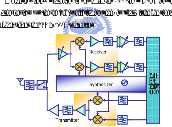
(20) Chapter 2. Frequency Synthesizer For IEEE 802.11a. 2.1 Role of Frequency Synthesizer for IEEE 802.11a Transceiver IEEE 802.11a is a popular wireless standard, and it has many specifications, of course, including the RF part, the transmitter mask and the ability of rejection for adjacent channel will define linearity and the sharp of signal. The receiver SNR will be required for demodulated in baseband part and the system sensitivity for all kinds of the date rate, and sensitivity and transmitter mask will define the dynamic range. Therefore, there are some specifications for RF transmitter and RF receiver. A generic wireless transceiver is shown in Fig. 2.1. The role of a frequency synthesizer is to provide the local oscillation frequency for transmitting and receiving channel signals in IEEE 802.11a Transceiver.. Receiver. Synthesizer. A/D D/A Inter -face. Transmitter. Fig. 2.1. 802.11a wireless LAN direct-conversion architecture.. For the frequency synthesizer, only the locking time, center frequencies and. 4.
(21) frequency accuracy have the specification to design. However, for typical wireless system, lower phase noise and lower sideband spurious tones will make the design of RF transmitter and RF receiver more easily because the transmitter mask and adjacent channel rejection are hard to design if large phase noise and large sideband spurious tones. In addition, output power is important issue because of the too small power of the frequency synthesizer will have less ability to drive the switch of the RF mixer and the actions for up-conversion and down-conversion will fail. In typical wireless system, the in-phase and quadrate paths are used for good modulation and demodulation, thus four phases synthesizer at least is required. Finally, the accuracy of the frequency synthesizer is another issue, for IEEE 802.11a standard, the carrier frequency offset is ± 20 ppm. Thus, the typical specifications for the frequency synthesizer are tuning range and locking time, frequency accuracy, phase noise, output power, quadrate phase, sideband spurious tones, stability, and power consumption.. 2.2 Specification of Frequency Synthesizer Locking Time The locking time for the IEEE 802.11a standard is 224us, this means the carrier switching time is less than 224us.. Phase Noise The phase noise is the important performance for the frequency synthesizer. Bad phase noise will block the desire signal due to the adjacent channel, thus, the good control for the phase noise is important. Fortunately, the phase-locked loop has the. 5.
(22) good performance on phase noise. Considering the system specification as the Fig. 2.2, for the each date rate, the each reference has given, for the worse case, minimum sensitivity is –82 dBm when the date rate is 6MHz per second, and thus considering the adjacent channel, the calculation about the phase noise is: L{ω m } = Pdseire − SNRmin − 10 log(20 MHz ) − Padjacent = −99dBc / Hz@20MHz offset frequency. For the non-adjacent channel, the phase noise can be calculated as –118dBc/Hz at 40MHz offset frequency. However, for the typical case, the phase noise of the desire frequency falls in VCO 1 / f. 2. region. Thus if the phase noise is –99dBc/Hz at offset. frequency 20MHz, then the phase noise at the offset frequency 40MHz is –99-10log22=-105dBc/Hz. Therefore, the phase noise should be defined as –118dBc/Hz at the offset frequency 40MHz or -112dBc/Hz at the offset frequency 20MHz, thus the specification about phase noise has been set. Non-Adjacent Channel -47 dBm. Adjacent Channel. -63 dBm. -63. -47 dBm dBm. Reference Level Reference Level:-79 /-78 /-76 /-74 /-71 /-67 /-63 /-62 dBm. Fig. 2.2. The spectrum of the system specification.. 6.
(23) Padjacent Pdseire Channel BW. SNR. Fig. 2.3. Out-band calculation of the phase noise. The noise discussed above is from out-band calculation, however, the in-band calculation should be taken in consideration, for non-ideal frequency synthesizer (with phase noise), the received signal will be convoluted with non-ideal LO signal and then the down converted signal will get worse SNR than ideal LO signal. Therefore, for consideration of in-band phase noise, the specification about phase noise is based on base-band modulation, for IEEE 802.11a standard, the signal modulation is OFDM and the required phase noise is about -90dBc/Hz at offset frequency 100kHz (From BB simulation). For this specification, is strict than out-band specification. Therefore, we will take in-band phase noise as specification. Additional, I, Q phase mismatch should less than 50 for correct demodulation.. 7.
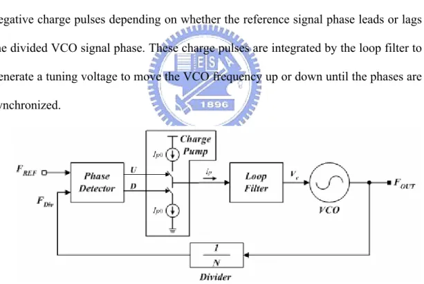
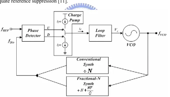
(24) Chapter 3 Review of Frequency Synthesizer Architecture 3.1 Basic PLL Operation A basic PLL consists of a reference oscillator, phase/frequency detector, charge pump, loop filter, voltage controlled oscillator(VCO) and divider. The reference oscillator is obtained often from a quartz, with a very accurate frequency. With a constant divisor of N, the loop forces the VCO frequency to be exactly N times the reference frequency. The phase/frequency detector and charge pump deliver either positive or negative charge pulses depending on whether the reference signal phase leads or lags the divided VCO signal phase. These charge pulses are integrated by the loop filter to generate a tuning voltage to move the VCO frequency up or down until the phases are synchronized.. Fig. 3.1. The block diagram of the synthesizer. PLLs are used as frequency synthesizers in many applications where it is necessary to generate a precise signal with low spurs and good phase noise. A VCO’s frequency may be changed by varying either the reference frequency or the divisor.. 8.
(25) But the reference is often a stable, fixed oscillator so it is the divisor that is varied in integer steps, such that Fout = N * Fref. One limitation with this type of PLL is that the VCO frequency cannot be varied in steps any smaller than that of the reference. With a little more circuitry, though, a 1/M divider could be placed between the reference and the phase/frequency detector, in which case the VCO output would be determined by the ratio of the integer divider, such that Fout = (N/M)*Fref. Even when the loop is locked the charge pump still outputs small charge pulses, caused by mismatches in the PLL’s positive and negative charge pumps and other factors such as non-ideal phase/frequency detection. These pulses create sidebands, or spurs, in the VCO output spectrum at offset frequencies equal to the reference. Dealing with these spurs requires design tradeoffs for fine frequency resolution we want a low reference frequency, but this will cause spurs to be generated closer to Fout and a tighter loop filter bandwidth is required to filter them. PLLs with tighter loop bandwidths have longer transient settling times (from one frequency to another.) Also, the narrower the loop bandwidth the less suppression there is of the VCO’s phase noise outside the loop bandwidth.. 3.2 Linear Model of PLL Although the PLL is nonlinear since the phase detector is nonlinear, it can accurately be modeled as a linear device when the loop is in lock. When the loop is locked, it is assumed that the phase detector output voltage is proportional to the difference in phase between its inputs; that is, Vd = K P (θ i − θ div ). 9. (3-1).
(26) where θ i and θ div are the phases of the input and divider output signals, Phase Detector & Charge Pump. θi. Loop Filter. KP. Z(s). VCO. KVCO s. θo. θ div 1 NDiv Divider. Fig. 3.2. Linear model of a PLL synthesizer. Respectively. K P is the phase detector gain factor and has the dimensions of voltage per radian. It will also be assured that the VCO can be modeled as a linear device whose output frequency deviates from its free-running frequency by an increment of frequency, ∆ω = K VCOVC. (3-2). where VC is the voltage at the output of the low-pass filter and K VCO is the VCO gain factor, with the dimensions of rad/s per volt. Since frequency is the time derivative of phase, the VCO operation can be described as ∆ω =. dθ o = K VCOVC dt. (3-3). With these assumptions, the PLL can be represented by the linear model shown in Fig. 3.2 [8]. Z(s) is the transfer function of the low-pass filter. The linear transfer function relating θ o ( s ) and θ i is H (s) =. K P Z ( s ) K VCO / N θo = θ i s + K p Z ( s ) K VCO / N. 10. (3-4).
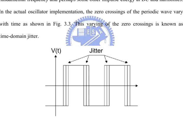
(27) If no low-pass filter is used, the transfer function is H (s) =. K P K VCO / N θo K = = , θ i s + K p K VCO / N s + K. K=. K P K VCO N. (3-5). which is equivalent to the transfer function of a simple low-pass filter with unity DC gain and bandwidth equal to K.. 3.3 PLL Noise Analysis The job of any frequency synthesizer is to generate a spectrally pure output signal. An ideal periodic output signal in the frequency domain has only an impulse at the fundamental frequency and perhaps some other impulse energy at DC and harmonics. In the actual oscillator implementation, the zero crossings of the periodic wave vary with time as shown in Fig. 3.3. This varying of the zero crossings is known as time-domain jitter.. Fig. 3.3. Periodic signal with jitter. A signal with jitter no longer has a nice impulse spectrum. Now the frequency spectrum consists of impulses with skirts of energy as shown in Fig. 3.4. These skirts are known as phase noise.. 11.
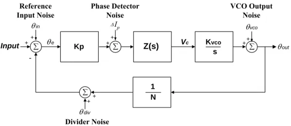
(28) Fig. 3.4. Frequency spectrum of a signal with phase noise. Phase noise is generally measured in units of dBc/Hz at a certain offset from the desired or carrier signal. The formal definition of phase noise is the ratio of the sideband noise power in a 1Hz bandwidth at a given frequency offset ∆ω from the carrier over the carrier power as shown in the following. L{∆ω } =. Psideband (ω o + ∆ω , 1Hz Bandwidth ) Pcarrier. (3-6). The PLL can be designed in such a way as to minimize the phase noise of the output signal. Fig. 3.5 shows the simplified PLL model with noise sources. The major noise sources of the PLL include an external reference input noise (θ in ), VCO internal noise ( θ vco ), phase detection noise ( ∆I p ), and frequency divider noise ( θ div ). The way the PLL is designed depends on what is the dominant source of noise in the loop.. 12.
(29) Reference Input Noise. θ in Input. +. +. ∑. VCO Output Noise. Phase Detector Noise ∆I p. θvco. +. θe. +. Kp. ∑. Z(s). Vc. -. Kvco s. +. +. ∑. θ out. 1 N. ∑ + +. θ div Divider Noise. Fig. 3.5. Simplified PLL model with noise sources. The transfer function of the output noise ( θ out ), due to each of the noise source, can be calculated as follows.. θ out =. I K Z ( s ) /(2πs ) 1 θ vco + P VCO θ I P K VCO Z ( s ) I P K VCO Z ( s ) in 1+ 1+ 2πNs 2πNs +. where N Kp. I P K VCO Z ( s ) /(2πs ) 1 I P K VCO Z ( s ) /(2πs ) θ div + ∆I p I P K VCO Z ( s ) I P K VCO Z ( s ) Kp 1+ 1+ 2πNs 2πNs. (3-7). value of the output divider, = I p 2π , the gain of the phase detector. KVCO ( dω / dv ), VCO gain, Z(s) transfer function of the loop filter, charge pump current. Ip If the transfer function Z ( s ) is denoted by Z ( s ) =. M ( z) where both M (z ) and N ( z). N (z ) are polynomials, then the (3.7) can be rewrote as:. θ out =. I K M ( s ) /(2π ) sN ( s ) θ vco + P VCO θ I P K VCO M ( s ) I P K VCO M ( s ) in sN ( s ) + sN ( s ) + 2πN 2πN. 13.
(30) +. I P K VCO M ( s ) /(2π ) 1 I P K VCO M ( s ) /(2π ) θ div + ∆I I P K VCO M ( s ) I P K VCO M ( s ) p Kp sN ( s ) + sN ( s ) + 2πN 2πN. (3-8). , when DC is under consideration, θ out = N (θ in + θ div + (1 Kp )∆I p ) , and this means that the spectrum of phase noise will be N 2 times the input noise and hence 20 log( N ) , and it is shown in Fig. 2.9. From equation (3-8), the output phase noise. due to phase noise of VCO is a high pass characteristic when N (s ) is a function of constant, or band pass behavior when N (s ) and M (s ) are higher order polynomial than function of constant. And the output phase noise due to the other source is a low pass characteristic. Taking third order PLL for example, the output phase noise is:. ⎞ ⎛ τs r s2C1⎜ + 1⎟ (τs + 1) /(2π ) I P KVCOC1 ⎝ r +1 ⎠ r +1 θout,3 = θvco + θin ⎞ I P KVCO r ⎞ I P KVCO r 2 ⎛ τs 2 ⎛ τs (τs + 1) (τs + 1) s C1⎜ s C1⎜ + 1⎟ + + 1⎟ + ⎝ r + 1 ⎠ 2πM r + 1 ⎝ r + 1 ⎠ 2πM r + 1 r (τ s + 1) / (2π ) I P K VCO C1 + 1 r + θ div ⎛ τs ⎞ I P K VCO r 2 (τ s + 1) + 1⎟ + s C1 ⎜ 2π M r + 1 ⎝ r +1 ⎠ r (τs + 1) / (2π ) I P KVCOC1 1 r 1 + ∆I p + (3-9) Kp 2 ⎛ τs ⎞ I P KVCO r (τs + 1) s C1⎜ + 1⎟ + 2πM r + 1 ⎝ r +1 ⎠ Phase noise. VCO only Overall phase noise. 20logM+ Nonlinear effect VCO after PLL fz1 Input only. Input after PLL fp1. 14. fp2. fm.
(31) Fig. 3.6. Output phase noise of a charge pump PLL with a frequency divider. , the transfer function of output phase noise has some points, at low frequency, I K r ⎞ ⎛ τs (τs + 1) , thus θ out ≈ N (θ in + θ div + (1 Kp)∆I p ) and + 1⎟ << P VCO s 2 C1 ⎜ 2πM r + 1 ⎝ r +1 ⎠. the. input. phase. noise,. or. other. noise. is. dominant,. and. at. high. I K r ⎞ ⎛ τs (τs + 1) , thus θ out ,3 ≈ θ vco and the noise frequency, s 2 C1 ⎜ + 1⎟ >> P VCO 2πM r + 1 ⎝ r +1 ⎠. from VCO is dominant. Although at low frequency, the output phase noise has been times N 2 , the crystal oscillator for input source has an excellent phase noise, the output phase noise has not caused much high phase noise. However, the choice of the frequency divide ratio still should be taken care and should not be taken a too large divide ratio. Additional, for high frequency wireless system, the VCO has a high frequency and large tuning range, this will make gain constant of VCO, K VCO , become very large. Therefore, the noise on control voltage of VCO is very important for overall output phase noise, thus there are many points to be taken care, one is layout consideration, the metal line of control voltage should be far from other circuit elements, and the noise from supply and resister of loop filter should be made sure that the thermal noise of these items do not cause too much noise peaking at low frequency while maintaining the low noise at higher frequency. The noise sources from the loop resister and supply can be expressed as follows:. φ ni v n1. =. φ no ,3 φ no ,3 sC1 sC1 ⇒ = ⋅ RC1 s + 1 v n1 RC1 s + 1 φ ni. (3-10). , where v n1 is the equivalent voltage noise of R , and the noise source from supply is the same with (3-10). Thus, too large value of the resister will make large voltage. 15.
(32) noise and have the influence on phase noise. From above analysis, we know that there are many kinds noise source in PLL system, some of them have a low pass characteristic, such as frequency divider, phase detector, resister of the loop filter, charge pump, and the other has a high pass characteristic, such as VCO. Therefore, good choice for loop filter can make noise optimized and makes the design of the mixer more easily in the whole transceiver. There is a well-known trade-off in the design of a PLL [9] between the loop bandwidth, jitter performance and the locking speed. If the loop bandwidth is large, the PLL takes little time for locking and has large jitter reduction of the internal VCO noise, but cannot have a good suppression of the external input noise. If, on the other hand, the loop bandwidth is small, the PLL can have large input jitter reduction, but takes longer time for locking and leaves much of the internal VCO noise unreduced. Therefore, it is desirable to optimize the loop bandwidth such that the PLL has sufficient noise reduction of both the external input and the VCO.. 3.4 Direct Digital Frequency Synthesizer When extremely fast switching speed of the synthesizer is required, as is the case for frequency-hopped systems, direct-digital frequency synthesis (DDFS) is a potential solution. The basic architecture is depicted in Fig. 3.7. φ. Fig. 3.7 Direct-digital frequency synthesis architecture. The basic operation is straightforward sine it is purely a feedforward system. By. 16.
(33) changing the value (K) of the frequency register, the phase will accumulate at a different speed and the frequency of the sine wave ROM output changes as a result. Therefore the synthesized output frequency is given by f out = f clk ⋅. K Lacc. (3-11). Where Lacc is the accumulator length and fclk is the reference clock frequency. The digital sine wave is sent through a digital-to-analog converter (DAC) and lowpass filtered to remove unwanted high-frequency content. Since DDFS is a feedforward system, the switching time is essentially instantaneous. The frequency resolution is determined by the word length in the phase accumulator and can be much less than 1 Hz. The output spurious tones are caused by truncation in the phase accumulator and are approximately equal to ⎛ 2 −2( k −1) ⎞ ⎟ Pspur (dB) = 10 log⎜⎜ ⎟ 3 ⎝ ⎠. (3-12). Where k is the input bit length of DAC. Therefore, if spurious levels of -56dBc are specified, the accumulator and DAC would require 10 bits of dynamic range. Several limitations to DDFS have restricted is application. First, the output frequency of the sine wave ROM is limited by the Nyquist criterion to half of the speed of the DAC. Furthermore, for low spurious levels, a very high-precision DAC is needed. The combination of high-speed and high-precision makes the power consumption too large to be useful in portable applications. To provide an RF carrier, the output of the DDFS must be mixed up using a single-sideband mixer with a fixed-frequency oscillator.. 17.
(34) 3.5 Integer-N and Fractional-N Frequency Synthesizer Fig. 3.8 shows the basic blocks of a PLL frequency synthesizer. For integer-N phase-locked loop (PLL) frequency conventional synthesizers, the phase detector comparison frequency must be equal to the channel spacing (frequency resolution) because the main divider (N) can only increment and decrement in integer steps. In this architecture of synthesizers the loop bandwidth and the frequency resolution are closely interrelated. A high frequency resolution inherently implies a small reference frequency, and thus a slow switching time [10]. As a rule of thumb, the loop bandwidth should be less than one tenth of the reference frequency to achieve adequate reference suppression [11].. Fig. 3.8. The block diagram of the synthesizer. The fractional-N PLL architecture allows frequency steps far smaller than the reference frequency. In other words, the main divider of the fractional-N synthesizer is capable of generating steps to be a fraction of the comparison frequency. Now the total divide ratio consists of an integer part ( N ) and fractional part ( NF Q ). The. 18.
(35) numerator ( NF ) and the denominator ( Q , either 5 or 8) of a fraction are controlled through software programming. The advantage of fractional-N synthesizers is two-fold. Since the close-in noise floor is directly related to total divided ratio (N), reducing N five or eight time theoretically implies a close-in noise floor improvement of 14dB(20log 5) or 18dB(20log8), respectively. At the same time, the comparison frequency will be 5 or 8 times great than it would be if a conventional synthesizer were used. This allows a wider loop filter to be used, that is to say, the loop bandwidth can be larger, alleviating the requirements for the voltage-controlled oscillator (VCO) phase noise and achieving a faster switching time. However, the fractional division causes spurious tones is shown in Fig. 3.9 at offset frequencies of n ⋅ fref , n = 1,2,....... F. where F is the denominator of the fractional divisor.. Fig. 3.9. Spurious tone. The loop filter attenuates these spurs, which restricts the loop bandwidth to reduce the spurs to an acceptable level. The result compared to integer-N is a wider loop bandwidth and an improvement in phase noise but at the cost of introducing unwanted spurs.. 19.
(36) 3.6 Delta-sigma Fractional-N Frequency Synthesizer Since the spurious noise of fractional-N synthesizer comes from periodical phase error contributed by PFD, eliminating the phase error before modulating the VCO is a possible solution. Several methods to overcome the spurious problem have been proposed [12], [13], [14], out of which the method of reducing the noise by using a delta-sigma ( ∆Σ ) modulator has shown to be most promising and to be widely accepted as the best one.. 3.6.1 ∆Σ Modulator Basics A general delta-sigma modulator and its linear model are shown in Fig. 3.10. Fig. 3.10(a) shows a block diagram of how the system is implemented with integrator circuits. The integrator is a switch-capacitor discrete-time integrator. The A/D converter can be implemented in many ways. In order to simplify the explanation, assuming the A/D converter is a simple 1-bit quantizer or comparator. The D/A converter take the digital output and convert it back to an analog signal that is subtracted from the input signal at the input to the integrator. This system can be represented by the discrete-time equivalent linear model shown in Fig. 3.10(b). The switch-capacitor integrator is represented by its transfer function H(z), and the feedback path represents the 1-bit D/A converter.. (a). 20.
(37) (b). Fig. 3.10 (a) general ∆Σ modulator and (b) linear model of the ∆Σ modulator Treating the linear model shown in Fig. 3.10(b) as having two independent inputs, input signal X(z) and quantization noise Q(z). We can derive a signal transfer function, STF (z), by setting Q(z)=0. S TF ( z ) =. H ( z) 1 + H ( z). (3-13). We can also derive a noise transfer function, NTF(z), by setting X(z)=0. N TF ( z ) =. 1 1 + H ( z). (3-14). From equation (3-14), as we have seen, the zero of the noise transfer function, NTF(z), will be equal to the poles of H(z). In other words, Then H(z) goes to infinity, we see equation (3-14) that NTF(z) will go to zero. We can also write the output signal as the combination of the input signal and the noise signal, with each being filtered by the corresponding transfer function. In the discrete frequency domain, we have corresponding transfer function. In the discrete frequency domain, we have Y ( z ) = S TF ( z ) ⋅ X ( z ) + N TF ( z ) ⋅ Q( z ). =. 1 H ( z) ⋅ X ( z) + ⋅ Q( z ) 1 + H ( z) 1 + H ( z). (3-15). To noise-shape the quantization noise in a useful manner, H(z) are properly chosen such that its magnitude is large from DC to f0 (i.e., over the frequency band of. 21.
(38) interest). With such a choice, the signal transfer function, STF (z), will approximate unity over the frequency band of interest. Furthermore, the noise transfer function, NTF(z), will approximate zero over the same band. In other words, NTF(z) will have a high-pass response. Thus the quantization noise is reduced over the frequency band of interest while the signal itself is unaffected.. 3.6.2 Higher-Order ∆Σ Modulator for Divider Control Ideally the divisor would be continuously variable, set arbitrarily, which would attain continuous frequency resolution, without spurs. Of course this is not possible because the divider must be set to integer values. In the fractional-N PLL, the desired fraction is converted by the accumulator to a sequence of 1s,0s and with overflow, which could be considered a coarse, 1-bit ADC. Fig 3.10 shows the basic modulator used in sigma-delta A-D converters x(k) is the modulator input, y(k) is the modulator output, and eq(k) is the quantization error added by the 1-bit A/D. In fractional-N synthesis application, the input to the delta-sigma modulator is the desired fractional offset, which is a digital word. Consequently, the integrator may be digitally implemented and the 1-bit D-A is not required. eq1(k ) x(t ). x(k ). y (k ). ∑ 1-bit A/D. 1-bit D/A. 22. Z −1.
(39) Fig. 3.11 Sigma-delta Modulator Fig.3.11 shows a sigma-delta modulator suitable for fractional-N synthesizer.. 1 1 1 − z −1 ( X ( z )) + Eq (z ) Y ( z) = 1 + z −1 1 + z −1 1 − z −1 1 − z −1. (. ). (. ). (. ). = X ( z ) + 1 − z −1 E q ( z ). (3-16). where Y(z), X(z) and Eq(z) are the Z-transforms of y(k), x(k), and eq1(k),respectively.. eq1(k). x(k). ∑. y(k). 1 1 − Z −1 1-bit Quantizer. Z −1. Fig. 3.12 Sigma-delta modulator for fractional-N synthesizer. Higher-order delta-sigma modulators improve the noise-shaping characteristic at low frequencies. The analysis of higher-order modulators are much more complicated than first order ones and given in literatures [15] [16]. Because the mathematical description for higher-order stability is difficult, the design of higher-order modulator is usually based on several empirical rules rather than analytical solutions [17]. Higher order modulators with several feedback are not always stables but this problem can be solved as the MASH (Multistage noise shaping technique) structure, proposed in the article [18]. A cascade of first-order modulator is used to shape progressively to a high degree the input. If we filter out the high frequency component H noise , the. 23.
(40) component X(z) remains. The total order of the modulator is fixed by the number of first-order modulators placed in cascade. Usually the third-order or fifth-order modulator is used. We will develop the equation associated with a third-order structure as shown in Fig. 3.13 and consider the practical implementation.. Fig. 3.13. Multistage noise shaping, in the MASH 1-1-1.. In Fig 3.12, the output y is expressed as a summation of different contributions from the input x =. K and several one-bit quantizers q1, q2 and q3, where for all i, qi F. is a quantization noise not correlated with the input and with the other noise sources. The expression of y is give by Y ( z ) = X ( z ) + Q1 (1 − z −1 ). 24.
(41) + (−Q1 + Q2 ( z )(1 − z −1 ))(1 − z −1 ) + (−Q2 + Q3 ( z )(1 − z −1 ))(1 − z −1 ) 2. = X ( z ) + (1 − z −1 )3 Q3 ( z ) = X ( z ) + H noise ( z )Q3 ( z ). (3-17). From the equation (3-17) we can deduce the frequency noise introduced by fractional division when the MASH3 controls the division ratio by N / N + 1 with x =. K and F. N given. Indeed ∫ vco = ( N int eger + N fractiona l ) f ref .From this term the constant term Nf ref +. K f ref is removed and the fluctuating term F. f noise ( f ) = H noise ( f )Q3 ( f ) f ref = Nf ref + (. K + H noise ( f )Q3 ( f )) f ref (3-18) F. remains, which is the expression of the frequency fluctuation noise introduced by fractional-N frequency synthesis. A 1-bit quantizer produces a quantization q3 which is uncorrelated with x . Furthermore if q3 is assumed to be a uniformly distributed white-noise sequence, the mean of q3 is zero and the variance is ∂ q 2 = 3. ∆ , with ∆ = 1 . As the power is 12. spread over the bandwidth f ref , the power spectral density (PSD) of the quantization. error q3 is. ∂ q3 2 fref. =. 1 . This enables us to write the expression of the 12 f ref. frequency fluctuation f noise ( z ) as. 25.
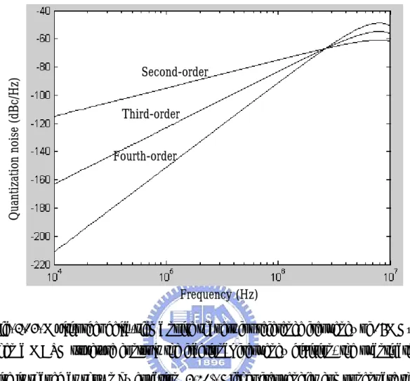
(42) S f noise = H noise ( f ) f ref. 2. 1 = 12 f ref. 1 − z −1. 6. f ref. 12. (3-19). In terms of noise contribution, the expression of the phase noise is more relevant than the frequency noise expression. Phase and frequency are related by an integration as φ = ∫ 2πf instantaneous dt Sφ , N ↔ N +1 ( z ) = S f. noise. 6. =. 1 − z −1 ⋅ f ref 12. ⋅. ⋅ S integration. (2π ) 2 1 − z −1 f ref 2. 4 (2π ) 2 1 − z −1 rad 2 / Hz = 12 f ref. (3-20). 2 f ref. In replacing z by e. f ref. , we can get:. (2π ) 2 πf 2 sin( ) Sφ , N ↔ N +1 ( f ) = 12 f ref f ref. 4. Generalizing equation (3-20) to any number of modulator sections;. S φ , N ↔ N +1 ( f ) =. (2π )2 12 f ref. [2 sin (πf. f ref. )]2 ( m −1) rad 2. Hz. (3-21). where m is the number of modulator sections. The phase noise contributed by the quantization noise of modulator for a reference frequency of 16 MHz is plotted with second-order, third-order and fourth-order structures is shown in Fig. 3.14.. 26.
(43) Quantization noise (dBc/Hz). Second-order Third-order Fourth-order. Frequency (Hz). Fig. 3.14. Multi-order delta-sigma noise shapers for reference frequency of 16MHz. When a MASH structure controls the fractional frequency division, the quantization noise is shaped as shown by equation (3-21). Higher frequencies component are then removed by the low-pass filter in the PLL. Obviously, the spurious performance is improved. A digital accumulator is a compact realization of DSM. The output of the accumulator is delayed by a latch and fed back to the input of the accumulator as in a delta-sigma modulator. The overflow is a 2-level signal corresponding to the quantized output of the modulator. An example of MASH3 structure is implemented using digital accumulators is shown in Fig. 3.15.. 27.
(44) Z −1 Bit stream. K. a. Σ + + overflow. b. Z −1. a. Σ + + overflow. b Z −1. a. overflow. b Z. −1. Z −1. fdiv. Fig. 3.15. MASH 1-1-1 implementation using digital accumulators.. 3.6.3 High-Order ∆Σ -Controlled Fractional-N Synthesizer The noise shaping technique can also be utilized in fractional-N frequency synthesis applications. A block diagram of a ∆Σ fractional-N synthesizer is shown in Fig. 3.16. The ∆Σ modulator output is on average K / 2 m cycles of the reference frequency Fref . The resulting output frequency is the Fout = (N+ K / 2 m ) Fref.. The modulator output controls the instantaneous division modulus of the prescaler, such that the mean division modulus is (N+ K / 2 m ), with the number (m) of bits of the ∆Σ modulator and the input word (K). The corresponding phase changes at the prescaler output are quantized, leading to possible spurious tones and quantization noise. By selecting higher order ∆Σ modulators, the spurious energy is whitened and shaped to high-frequency noise, which can be removed by the low-pass loop filter. As a result, for a given frequency resolution, an arbitrary high Fref can be chosen, by assigning the proper number of bits K to the modulator. The loop bandwidth is not restricted by the reference spur suppression, resulting in faster settling and higher integratability. Additionally, the division modulus is decreased by a factor 2 m _ min (with m_min the. 28.
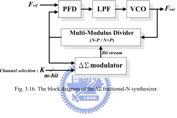
(45) minimum number of bits for the frequency resolution), so that noise of the PLL blocks, except for the VCO, is less amplified. It is worth pointing out that the delta-sigma modulator can be implemented using all digital architectures thus is easily integrated into single chip and is insensitive to process variation.. Fig. 3.16. The block diagram of the ∆Σ fractional-N synthesizer.. 29.
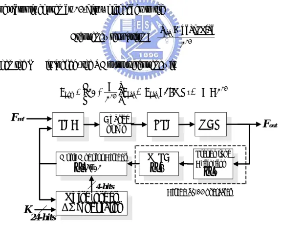
(46) Chapter 4. Circuit Level Implementation of. Frequency Synthesizer 4.1 Synthesizer Architecture The designed frequency synthesizer for 802.11a transceiver uses ∆Σ fractional-N method. Fig. 4.1 shows the block diagram of the designed frequency synthesizer. It is made up of multi-modulus prescaler and a third-order sigma-delta modulator, which is one of the noise shaping techniques to suppress the fractional spurs occurring at all multiples of the fractional frequency resolution offset. The input bit length of the modulator is chosen as 24-bits which leads to the Frequency resolution =. f ref × prescaler 2 24. When the PLL is locked, the RF output frequency is K ⎞ ⎛ Fout = ⎜ 20 + 24 ⎟ Fref , Fref =16MHz, 2 ⎠ ⎝. Fref. Charge pump. PFD. LPF TSPC. Multi-Modulus Divider. ÷17~24. ÷8. 4-bits. K. K < 2 24. VCO Pseudo type D-flip-flop. ÷2. Divide-by-16 prescaler. Third-order ΔΣmodulator. 24-bits. f. Fig. 4.1. The block diagram of the designed synthesizer.. 30. Fout.
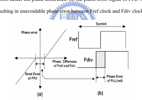
(47) 4.2 The Phase Detector One of the critical building blocks of the PLL is the phase frequency detector (PFD). An ideal phase detector produces an output signal whose DC value is linearly proportional to the difference between the phases of two periodic inputs. A low precision PFD has a wide dead zone (undetectable phase difference range), which results in increased jitter [19]. The jitter caused by the large dead zone can be reduced by increasing the precision of the phase frequency detector. Fig. 4.2 shows the relation between dead zone of PFD and the phase error of PLL. If the phase difference of Fref clock and Fdiv clock is smaller than the dead zone, the PFD cannot detect the phase difference. So the phase error signal of PFD will remain zero, resulting in unavoidable phase error between Fref clock and Fdiv clock.. Fig. 4.2. (a) PFD dead zone and (b) PLL jitter. In order to speed up the operation frequency and to reduce the dead zone, a dynamic logic style PFD was designed and shown in Fig. 4.3. From the circuit diagram of the PFD we can see that the shortened feedback path delay and dynamic operation allow high precision in the high-frequency. In order to avoid dead zone, the. 31.
(48) PFD asserts both UP and DW outputs as shown in Fig. 4.4. For in-phase inputs of Fref and Fdiv, the charge pump will see both UP and DW pulse for the same short. period of time. If there is a phase difference between Fref and Fdiv, the width of UP and DW pulse will be proportional to the phase differences of the inputs. The physical layout of the phase detector is shown in Fig. 4.5 and the performance summary of phase detector is listed in Table 1.. Fig. 4.3. The schematic of the phase detector.. Fig. 4.4. Waveform of the phase detector.. 32.
(49) Fig. 4.5. Physical layout of phase detector. Table 1 Performance summary of phase detector. Operation frequency. 16MHz. Power consumption. 0.36mW. Chip area. 50 × 16.2 um. 2. 4.3 Charge Pump In a conventional CP of fig. 4.6(a), several spikes occur on the output when the currents are switched on and off as switches M1 and M2 are directly connected to the output. These spikes reflect into the output if no proper actions are taken. As these spikes occur at the reference frequency, they will cause spurs in the PLL output spectrum at an offset from the carrier equal to reference frequency. In this design, to reduce the reference frequency spurs problem, we use indirectly connected switches M1 and M4 with output and thus the drain node of M2 and M3 is directly connected to the output which shown in Fig. 4.6(b). The current glitches that now occur at the sources of M2 and M3 when switching M1 and M4 would not be directly conveyed to the output node because M2 and M3 are still off when the. 33.
(50) glitches occur [20].. (a). Vbias. (b). Fig. 4.6. (a) Conventional charge pump (b) The schematic of the current source employed in the charge pump. The simulated result of charge and discharge current is show in Fig. 4.7. In this simulation UPB and DW signal are 1.8V 16MHz square waves. A capacitor 10nF loads the output of the charge pump. The charge pump positively charges the load capacitor with IUP when M1 turn on, M4 turn off and negatively charges the load capacitor with IDW when M1 turn off, M4 turn on. From the simulation result, the charge and discharge current is almost symmetric when referring to the vertical. 34.
(51) centerline (0.9V). It is means that the charge and discharge current match to each other. This better matching between the charge and discharge current will improve the sideband spurs. The physical layout of the charge pump is shown in Fig. 4.8.. Fig. 4.7 Simulation result of charge and discharge current.. Fig. 4.8. Physical layout of charge pump.. 4.4 Loop Filter The loop filter schematic is shown in Fig. 4.9. It consists of two resistors (R1 and R2) and three capacitors (C1, C2, and C3).. 35.
(52) ip. R2 R1. C2. Vc. C3. C1. Fig. 4.9. Third-order loop filter. The transimpedance of this loop filter is 1 + sτ 1 V C1 + C 2 + C3 1 Z (s) = c = ⋅ C τ + C 2 (τ 1 + τ 3 ) + C3τ 1 C2 Ip s + s 2τ 1τ 3 1+ s 1 3 C1 + C 2 + C3 C1 + C 2 + C3. (4-1). where τ 1 = R1C1 and τ 3 = R3C3 . In the filter, there are three poles and one finite zero. The locations of the poles and zero can be approximated for the case of C1 >> C2, C3 and R1 > R2 as 1 R1C1 =0. ωz =. (4-2). ω p1. (4-3). ω p2 ≈. 1. (4-4). R1 ( C 2 + C 3 ). and. ω p3 ≈. 1 . R3C 2 C 3 C 2 + C3. (4-5). One additional pole at the origin in the PLL comes from the VCO. The PLL -3dB bandwidth ω −3dB , which is equal to its open-loop unity gain ω u , must be placed somewhere between ω z and ω p 2 to obtain a reasonable phase margin for the PLL loop stability. Assuming that ω u = ω z ω p 2 and ω p 3 >> ω u , then the phase margin. 36.
(53) yields ⎛ ω p2 ⎜ ωz ⎝. Φ m ≈ arctan⎜. ⎞ ⎛ ⎟ − arctan⎜ ω z ⎜ ω p2 ⎟ ⎝ ⎠. ⎞ ⎟. ⎟ ⎠. (4-6). In Fig. 4.9, C1 produces the first pole at the origin for the type-II PLL. This is the largest capacitor, hence, it is a key integration bottleneck of the PLL. R1 and C1 are used to generate a zero for loop stability. C2 is used to smooth the control voltage ripples and to generate the second pole. Usually, the loop filter of the PLL consists of C1, C2 and R1. However, additional RC low pass filter is introduced to reduce any. “spurs” caused by the reference frequency and to reduce the high frequency noise which is mainly caused by the undesired narrow pulses from the PFD due to the delay. Table 2 gives the selected component values. The design value of R2 and C3 is optimized based on area on the chip and locking time. The R2C3 time constant should be large for a low cutoff frequency. However, if a large R2 and C3 is added, the total step response also changes a lot. When the value of R2 and C3 is somewhat lower than the one of R1 and C2, respectively, the whole response does not change too much. Therefore, the product of R2 and C3 should be about half of the R1 and C2. Table 2: PLL pole, zero and loop bandwidth parameters Reference frequency. f ref. 16 MHz. PLL loop bandwidth. K. 281 KHz. Zero frequency. fz. 113 KHz. Second pole frequency. f p2. 1.21 MHz. Third pole frequency. f p3. 7.96 MHz. 37.
(54) Phase margin. Φm. 54°. f ref Attenuation. SpurAtten. 63.65dB. Elements:. R1. 22 kΩ. C1. 65 pF. C2 R2. 4 pF 15 kΩ. C3. 2 pF. 4.5 Spiral-Inductor LC-Tank VCO The quality of an LC-tank oscillator relies the quality of the LC-tank, which is the most important part of the oscillator concerning its quality. Therefore, the ideal oscillator would have infinite quality factor LC-tank. In practice, the quality factor of inductors is not very high in CMOS standard processes. The negative resistance is needed to compensate the tank with energy and sustain the oscillator. A feedback oscillator of Fig. 4.10 shows the implementation of a basic current steered LC-tank oscillator, which is designed to keep the transistors always in saturation. When the cross-coupled pair is close to clip the amplitude, one node is high and the other one is low. The negative resistance is typical provided by a cross-coupled pair of PMOS transistors, Q1 and Q2. Calculating the impedance seen at the drain of Q1 and Q2, it is noted that the positive feedback yields Rin = −. 2 gm. (4-7). Simultaneously, the frequency of this circuit is given by f osc =. 1 2π LC. ,. (4-8). 38.
(55) where C represents the sum of all capacitance at the output node. Thus, if Rin is less than or equal to the equivalent parallel resistance of the tank, the circuit oscillates. This topology is called a “negative-gm oscillator”.. IBosc. Q1. C. IBosc. Q2. L. L. Q1. Q2. C Rin. Fig. 4.10. Differential LC-tank oscillator schematic. The relationship between oscillator phase noise and quality factor can be expressed by Leeson’s phase-noise model which is shown in the following. ⎧⎪ 2 FkT L(∆f ) = 10 log ⎨ ⎪⎩ Psig. ⎡ ⎛ f ⎢1 + ⎜⎜ o ⎢⎣ ⎝ 2Q∆f. ⎞ ⎟⎟ ⎠. 2⎤. ⎛ ∆f1 / f 3 ⎥ ⋅ ⎜1 + ∆f ⎥⎦ ⎜⎝. ⎞⎫⎪ ⎟⎬ ⎟ ⎠⎪⎭. (4-9). Where L(∆f ) is SSB noise spectral density in units of dBc/Hz. The symbol k is Boltzman’s constant, T is temperature in Kelvin, F is the excess noise factor, f o is the carrier frequency, ∆f1 / f 3 is the corner where the spectrum becomes proportional to 1 / f 3 , and Psig is the output signal power of the oscillator. The designed quadrature VCO schematic is shown in Fig. 4.11 [21]. Since the constant Gm current source can improve the phase noise [22], the constant Gm. 39.
(56) current bias circuit is employed to mirror the biasing current into the VCO core. The negative resistor in Fig. 4.11 is realized by two cross-coupled PMOS transistors M1(M3) and M2(M4) to provide enough negative resistance for oscillation. The cathodes of the two junction varactors are connected together. Through Vc, the dc bias voltages of the two junctions can be adjusted to change the value of junction capacitance and, thus, the VCO frequency. Since the quadrature error depends on the duty cycle of the VCO, special attention is paid to the symmetry of the VCO layout which is shown in Fig. 4.13, 4.14. The pair of PMOS transistors is used to generate negative gm to overcome the loss of the LC tank, for two reasons. First, in this fabrication process, PMOS has lower device flicker noise than that of the NMOS. Furthermore, the PMOS resides inside an N-well and is well isolated from the noisy Si substrate. Despite its lower mobility,. PMOS is favored in this design due to low noise considerations. Fig. 4.12 shows the output buffer used to amplify the VCO output. It is a regular open drain circuit with an n-well resistor to bias the gate of the output transistor. The gate bias was set to 1.1V. The output was connected to a bias the tee and fed with 1.8V. The total current dissipation of the output buffer is about 5mA. The LC tanks of the VCO are formed using a ~0.78313nH circular shape of spiral inductor having center hole 165 µm, metal width 20 µm, turn 1.5, and 812.64fF P+/N-well varactor.. 40.
(57) Fig. 4.11. VCO schematic.. Fig. 4.12. Schematic of the output buffer.. Fig. 4.13. Physical layout of the spiral-inductor LC-tank VCO.. 41.
(58) Fig.4.14. Physical layout of VCO (enlarge the center part). The simulation I, Q channel outputs of the quadrature VCO at voltage control 0.8V are shown in Fig.15. The phase error is less than 0.5° and the amplitude error are less than 0.5%.. 42.
(59) m10 time=99.36nsec PPOUT3=272.5mV m11 m10. m11 time=99.31nsec PPOUT1=272.4mV 300. PPOUT3, mV PPOUT1, mV. 200 100 0 -100 -200 -300 99.0. 99.3. 99.5. time, nsec. (a). 300. PPOUT4, mV PPOUT2, mV PPOUT3, mV PPOUT1, mV. 200 100 0 -100 -200 -300 99.0. 99.3. 99.5. time, nsec. (b) m7 freq=5.299GHz dBm(Spectrum2)=-3.34 m7 -5. dBm(Spectrum2). m10 freq=10.56GHz dBm(Spectrum2)=-31.84 -25. m10. -45. -65 22.0. 21.5. 21.0. 20.5. 20.0. 19.5. 19.0. 18.5. 18.0. 17.5. 17.0. 16.5. 16.0. 15.5. 15.0. 14.5. 14.0. 13.5. 43. 13.0. (c). 12.5. 12.0. 11.5. 11.0. 10.5. 10.0. 9.5. 9.0. 8.5. 8.0. 7.5. 7.0. 6.5. 6.0. 5.5. 5.0. 4.5. 4.0. 3.5. 3.0. 2.5. 2.0. 1.5. 1.0. freq, GHz.
(60) m7 freq=5.299GHz dBm(Spectrum2)=-3.33 m7 -5. dBm(Spectrum2). m10 freq=10.56GHz dBm(Spectrum2)=-32.81 -25. m10. -45. -65 22.0. 21.5. 21.0. 20.5. 20.0. 19.5. 19.0. 18.5. 18.0. 17.5. 17.0. 16.5. 16.0. 15.5. 15.0. 14.5. 14.0. 13.5. 13.0. 12.5. 12.0. 11.5. 11.0. 10.5. 10.0. 9.5. 9.0. 8.5. 8.0. 7.5. 7.0. 6.5. 6.0. 5.5. 5.0. 4.5. 4.0. 3.5. 3.0. 2.5. 2.0. 1.5. 1.0. freq, GHz. (d) Fig. 4.15. The simulation I, Q channel outputs of the VCO with quadrature phase output (a) single mode (b) differential mode (c) I channel spectrum (d) Q channel spectrum. The simulated VCO tuning characteristic and output power is shown in Fig. 4.16, Fig. 4.17, respectively. Its tuning range is about 610MHz (from 4.92GHz to 5.53GHz) for 1.8V operation, which yields The VCO gain (KVCO) about 450MHz/V. m 1 V b d c =0 .4 0 0 fr e q [ : : , 1 ] = 5 . 1 4 9 E 9. m 2 V b d c = 1 .0 0 0 fr e q [ : : , 1 ] = 5 . 3 5 7 E 9. 5 .6 0 G 5 .5 0 G. m2. freq[::,1], Hz. 5 .4 0 G 5 .3 0 G. m1. 5 .2 0 G 5 .1 0 G 5 .0 0 G 4 .9 0 G 0 .0. 0 .1. 0 .2. 0 .3. 0 .4. 0 .5. 0 .6. 0 .7. 0 .8. 0 .9. 1 .0. 1 .1. 1 .2. 1 .3. 1 .4. 1 .5. 1 .6. 1 .7. 1 .8. Vbdc. Fig. 4.16. The simulated VCO tuning characteristic.. 44.
(61) -1.50. m8 m9 Vbdc=0.400 Vbdc=1.000 dBm(PPOUT1[::,1])=-3.250dBm(PPOUT1[::,1])=-2.269. dBm(PPOUT1[::,1]). -2.00. m9. -2.50 -3.00. m8. -3.50 -4.00 -4.50 -5.00 0.0 0.1 0.2 0.3 0.4 0.5 0.6 0.7 0.8 0.9 1.0 1.1 1.2 1.3 1.4 1.5 1.6 1.7 1.8. Vbdc. Fig. 4.17. The simulated VCO output power. Fig 4.18 is phase noise with tuning voltage 0.8V, and phase noise is -92.41dBc/Hz at offset frequency 100KHz. The performance summary of VCO is tabulated in Table 3.. m3 noisefreq=100.0kHz N2.pnfm=-92.41 dBc. m5 noisefreq=100.0 Hz N2.pnfm=-7.730 dBc. 100. N2.pnmx, dBc N2.pnfm, dBc. 50. m5. 0 -50. m3. -100. m4 noisefreq=1.000MHz N2.pnfm=-112.9 dBc m4. -150 1. 1E1. 1E2. 1E3. 1E4. 1E5. 1E6. noisefreq, Hz. Fig. 4.18. The phase noise simulation of VCO. Table 3 : Performance summary of VCO. Parameter. Simulation (TT). 45.
(62) DC supply voltage. 1.8V. Varactor type. P+/N-well varactor. Output Power. ≈ -4dBm. Sweep frequency. 4.92~5.53GHz. Sweep voltage. 0V~1.8V. Turning range. 610MHz. Maximum VCO gain(Kvco). 450MHz / V -92.42@100KHz. Phase noise. -113@1MHz 6mW (core). Power consumption. 21mW (total) 2. 900 × 800 um. Chip area. 4.6 Frequency Divider 4.6.1 Divide-By-16 Prescaler The divide-by-16 circuit essentially has 4 divide-by-2 blocks cascaded one after another. In experience, the prescaler circuit will waste much more power if it direct operates at 5GHz RF signal without a divide-by-two circuit. The prescaler is actually a high-speed digital circuit, implying that its power consumption is proportion to CLV 2. f. The main trade-off in prescaler design is between speed and power. For low power. and high speed consideration, the feedback divide-by-16 prescaler is composed of a pseudo-NMOS type divider and a true-single-phase-clock (TSPC) based frequency divider [23]. The challenge was to design the first divide-by-2 circuits in such a manner so that they will have differential outputs and will be able to divide a frequency of around 5.4 GHz. In order to handle RF signal, the first divide-by-2 circuit apply pseudo-NMOS gates enables high-speed operation while providing large. 46.
(63) output swing. The pseudo-NMOS circuits use for a pull-up network only one PMOS as resistive load. The PMOS is operated in the strong inversion region by connecting its gate to ground, resulting in the advantage of reduced load capacitance, less interconnection and smaller area over standard CMOS. For the improved performance, we have to pay the cost of higher leakage current and less noise margin compared to the standard CMOS. Fig. 4.19 shows two pseudo-NMOS D-flip-flop (DFF) whose output are connected back to its inputs to form a ÷ 2 stage. In order to have the inputs vary around the switching threshold of the gates, CLK and CLKB are ac coupled through 0.2pf capacitors. An inverter whose input and output are tied together biases the DFF inputs to the correct dc level over process and temperature. Fig. 4.16 shows the result of the simulation of the divide-by-two circuit. Since the divide-by-two input are differential signal (CLK, CLKB), every differential signal path must match with each other. This means we must be careful when device placement and routing. As shown in Fig. 4.21, layout of this circuit is symmetric when referring to the horizontal centerline.. 47.
(64) Fig. 4.19. Pseudo-NMOS divide-by-two.. 1.6. 1.5 1.4. 1.3. OUTB, V clkp, V. 1.2. 1.1 1.0. 0.9 0.8. 0.7 0.6. 0.5 0.4 98.5. 99.5. time, nsec. 0.7. m1. mag(Spectrum) mag(Spectrum2) mag(Spectrum1). 0.6 0.5. m1 freq=3.000GHz mag(Spectrum1)=0.598 m2 freq=6.000GHz mag(Spectrum)=0.150. 0.4 0.3. m2. 0.2 0.1 0.0 2.0. 2.5. 3.0. 3.5. 4.0. 4.5. 5.0. 5.5. 6.0. 6.5. freq, GHz. Fig. 4.20 Divide-by-2 circuit simulation output with 6GHz input.. 48. 7.0.
(65) Fig. 4.21. Physical layout of divide-by-two. Following figure shows the result of the simulation of the divide-by-16 prescaler circuit. It has been calculated that the circuit consumes around 14mA of current. The performance summary of divide-by-16 is listed in Table 4.. 49.
數據
+7

相關文件
z 香港政府對 RFID 的發展亦大力支持,創新科技署 06 年資助 1400 萬元 予香港貨品編碼協會推出「蹤橫網」,這系統利用 RFID
An OFDM signal offers an advantage in a channel that has a frequency selective fading response.. As we can see, when we lay an OFDM signal spectrum against the
• This program constructs an instance of the device and prints out its properties, such as detected.. daughterboards, frequency range,
Compensates for deep fades via diversity techniques over time, frequency and space. (Glass is
This design the quadrature voltage-controlled oscillator and measure center frequency, output power, phase noise and output waveform, these four parameters. In four parameters
傳統的 RF front-end 常定義在高頻無線通訊的接收端電路,例如類比 式 AM/FM 通訊、微波通訊等。射頻(Radio frequency,
This research investigated the effects of frequency and lifting/lowering heights on the maximal acceptable weight of handling (MAWH) and perceived exertion when wearing
Direct Digital Frequency Synthesizer has many advantages of faster frequency switching, lower memory size, lower circuit complication, lower noise, higher frequency
