國
立
交
通
大
學
電機學院 電信學程
碩 士 論 文
衛星遙測系統之影像處理軟體與介面硬體設計
Design of Post-Processing Software and
Interface Hardware for Imagers
in Satellites’ Remote Sensing System
研 究 生:蔡銘晃
指導教授:闕河鳴 教授
衛星遙測系統之影像處理軟體與介面硬體設計
Design of Post-Processing Software and Interface Hardware for
Imagers in Satellites’ Remote Sensing System
研 究 生:蔡銘晃 Student:Ming-Huang Tsai
指導教授:闕河鳴 Advisor:
Her-Ming Chiueh
國 立 交 通 大 學
電機學院 電信學程
碩 士 論 文
A Thesis
Submitted to College of Electrical and Computer Engineering
National Chiao Tung University
in partial Fulfillment of the Requirements
for the Degree of
Master of Science
in
Communication Engineering
July 2009
Hsinchu, Taiwan, Republic of China
衛星遙測系統之影像處理軟體與介面硬體設計
學生:蔡銘晃
指導教授:闕河鳴博士
國 立 交 通 大 學
電 機 學 院 電 信 學 程 碩 士 班
摘
要
在現今的衛星遙測系統上高解析度影像重組與處理技術扮演很重要的角色。本研究 展示一個影像重組與處理系統,具有處理多個一維(直條狀)的 CMOS 影像感測器之能 力。此系統的優點在於可隨衛星線性移動特性來控制 CMOS 影像感測器合理的曝光時 間並提供即時的高解析度影像。
此系統的主要功能包含使用 ICAI (Image Combiner and Acquisition Interface) 晶片來 處理 CMOS 影像感測器的原始資料、於顯示器即時顯示影像、儲存影像與影像後處理 軟體。ICAI 晶片的功能在於同時處理多個直條狀的 CMOS 影像感測器資料流以及控制 CMOS 影像感測器動作。顯示與儲存影像是由一個 FPGA 開發板以硬體完成。此 FPGA 開發板同時整合了 ICAI 與其他週邊裝置,成為一個簡單的嵌入式系統,此嵌入式系統 可獨立完成從影像擷取到存檔的動作。 此系統的另一個部份為影像後處理軟體。因為此系統使用多個 CMOS 影像感測器以 建構高解析度影像,在封裝多個 CMOS 影像感測器的過程中,會造成一些影像的失真, 主要原因在不同 CMOS 影像感測器之間的特性差異與封裝誤差。此影像後處理軟體提 供一個在 PC 上運作的解決方案。 此軟體也提供了影像壓縮的功能,主要是可將嵌入式系統儲存的 Bitmap 檔案轉換為 HD Photo 檔案,HD Photo 是由微軟提出的高壓縮比與高影像品質的影像格式,應當非 常適合使用在此具有高存儲容量需求的衛星影像上。 關鍵字:遙測、影像重組、影像感測器、嵌入式系統。 i
Design of Post-Processing Software and Interface Hardware for
Imagers in Satellites’ Remote Sensing System
Student:Ming-Huang Tsai
Advisors:Dr.
Her-Ming Chiueh
Degree Program of Electrical and Computer Engineering
National Chiao Tung University
ABSTRACT
High resolution image combination and processing plays an important role in today’s satellites’ remote sensing application. The study presents an image recombination and processing system for one-dimensional multi-strip CMOS image sensors. The proposed system takes advantage of satellites’ linear moving property to control exposed time of CMOS image sensors and provide the real-time ability to generate high resolution image.
Briefly, the main functions of the system are processing image raw data by ICAI (Image Combiner and Acquisition Interface) chip, displaying image to VGA port, saving image file and post-processing image file in software. The multi-strip CMOS image sensors capture image and send signals to ICAI chip. The data stream and control of CMOS image sensors are dominated by ICAI chip. The VGA output and data processing are implemented on a FPGA development board. The FPGA development board integrates ICAI and necessary peripherals as an embedded system. The embedded system could independently complete the job from capturing to saving image.
The other part of the system is a software of image post-processing. Because the system uses multiple CMOS image sensors to construct larger image, there are some issues after packaging multiple sensors. The main issues are characteristics variation among sensors and package mismatch. The post-processing software provides a PC-based solution to overcome these problems.
The software also provides a function of image compression. The function is converting bitmap file to HD Photo file. HD Photo is a high compression rate and high quality image format developed by Microsoft Corporation. The advantages of HD Photo are very suitable for lager storage request in satellites’ application.
Keywords:remote sensing, image combination, image sensor, embedded system, HD Photo.
誌
謝
感謝闕河鳴老師的指導與鼓勵,讓本人在跌跌撞撞中把論文完成,也要感謝三位口 試委員-邱進峰博士、謝志成博士、林俐如博士願意在百忙之中對本人的論文提出指 教,讓論文內容與軟體實現可以更接近實際系統的需求。感謝師門郭振旗、劉嘉儀、陳 燦杰的幫忙與台科大翁誌暉的協助,當然還要感謝在交大期間幫助過我的同學與學弟。 唸了第二個碩士學位,雖然還是覺得自己的專業能力必須再加強,但還是感謝所有在交 大教過我的老師,給我一個良好的教學內容與過程。最後感謝家人的扶持與同事的工作 代理,讓本人可以順利趕上論文的時程。 iii
Contents
摘要 ………
i
Abstract ………
ii
誌謝 ……… iii
Contens ………
iv
Lists of Table ………
vi
Lists of Figure ……… vii
Chapter 1
System Overview ………
1
1.1
Introduction
………
1
1.2
Component and Platform ………
3
1.2.1
System Block Diagram ………
3
1.2.2 Sensor ………
4
1.2.3 ICAI
………
5
1.2.4
Integrator by FPGA Development Board ………
6
1.2.5
Host Computer and Image Post-Processing Software ………
7
1.2.6 Sensor
Emulator
………
8
Chapter 2
Hardware Architecture ……… 10
2.1
Hardware
Architecture of FPGA Board ……… 10
2.2
Nios II CPU ……… 11
2.3
Avalon Bus ……… 12
2.4
VGA
controller
……… 14
2.5
ICAI
controller
……… 14
2.5.1 ICAI
Protocol ……… 14
2.5.2 ICAI
Controller
Architecture
……… 17
2.6
Multi-Port SDRAM Controller ……… 18
Chapter 3
Software Architecture ……… 19
3.1
Software
Platform
……… 19
3.1.1
GUI Software ……… 19
3.1.2
HD Photo Software Development ……… 19
3.1.3
Software Flow ……… 19
3.2
Problems in the Sensor Array ……… 20
3.3
Calibration Method after Sensors Package ……… 23
3.3.1 Calibration
Flow ……… 23
3.3.2
Calibration for Gray-Level Variation ……… 24
3.3.3
Calibration for Package Offset and Overlap ……… 25
3.3.4
Calibration for Oblique Alignment ……… 27
3.4
Gray-Level Shifting ……… 28
3.4.1 Gray-Level
Difference among Sensors ……… 28
3.4.2
Gray-Level Shifting Function ……… 28
3.5
Image Overlap Cancellation ……… 29
3.5.1
Image Overlap from the Sensor Arrangement ……… 29
3.5.2
Image Overlap Function ……… 30
3.6
Package Offset Cancellation ……… 31
3.6.1 Package
Offset
from
the Sensor Arrangement ……… 31
3.6.2
Package Offset Cancellation Function ……… 31
3.7
HD Photo File Conversion ……… 32
3.7.1
Introduction to HD Photo ……… 32
3.7.2
HD Photo Encoding Process ……… 33
3.7.3
Comparison among HD Photo, JPEG, JPEG2000 ………… 34
3.7.4
HD Photo Encoder Function ……… 35
Chapter 4
Experimental and Testing Results ……… 37
4.1
Hardware Experimental Result ……… 37
4.1.1
Hardware Simulation ……… 37
4.1.2 Hardware
Experiment ……… 38
4.2
Software
Operation ……… 39
4.2.1 Introduction
for
Software GUI ……… 39
4.3
Software
Test
……… 42
4.3.1 ‘Gray-Level
Shifting’ Function Test ……… 42
4.3.2 ‘Overlap
Cancellation’ Function Test ……… 43
4.3.3
‘Package Offset Cancellation’ Function Test ……… 43
4.3.4
‘Convert to HD Photo File’ Function Test ……… 45
Chapter 5
Conclusion and Future Work ……… 47
5.1
Conclusion
……… 47
5.2
Future Work ……… 47
Reference ……… 48
Lists of Table
Table 1 Logic table of ICAI ………
15
Table 2 Function of programmable registers ………
16
Table 3 (I) Hadamard transform, (II) one-dimension rotation transform
and (III) two-dimension rotation transform ………
34
Table 4 Performance of HD Photo, JPEG, JPEG2000 [1] ………
35
Table 5 Features and Functions of HD Photo, JPEG, JPEG2000 [1] ……
35
Table 6 Main parameters of HD Photo encoder ………
36
TABLE 1
Lists of Figure
Figure 1
Concept of satellite system ………
1
Figure 2
Block diagram of remote sensing satellite ………
2
Figure 3 System block diagram ………
4
Figure 4
Interleaved alignment of sensors and x-y axes definition ………
4
Figure 5
ICAI architecture ………
5
Figure 6
Process flow of combining image ………
6
Figure 7
Photograph of DE2-70 ………
7
Figure 8
Block diagram of DE2-70 ………
8
Figure 9
The configuration of two dual-port memory ………
9
Figure 10 The applied interpolation concept in sensor emulator …………
9
Figure 11 System block of Integrator by FPGA board ……… 11
Figure 12 Block diagram of NIOS II Soft-Core ……… 12
Figure 13 Architecture of Avalon Bus ……… 13
Figure 14 Read protocol of Avalon Bus (wait 1 cycle) ……… 13
Figure 15 Write protocol of Avalon Bus (no wait) ……… 13
Figure 16 Architecture of VGA controller ……… 14
Figure 17 ICAI to host computer interface ……… 15
Figure 18 Timing Diagram of configuring ICAI ……… 15
Figure 19 Timing diagram of reading one-line image data ……… 17
Figure 20 Timing diagram of reading full 2D image ……… 17
Figure 21 Architecture of ICAI controller ……… 18
Figure 22 Architecture of multi-port SDRAM controller ……… 18
Figure 23 Software flow chart ……… 20
Figure 24 Sketch graph of package offset and overlap ……… 21
Figure 25 Sketch graph of oblique alignment ……… 22
Figure 26 Vignetting effect in corners of photograph ……… 22
Figure 27 Vignetting effect for scanning a fully white image by the sensor
array ………
23
Figure 28 Calibration flow for sensor array ……… 24
Figure 29 Ideal and real gray-level mapping ……… 25
Figure 30 linear transform between ideal and real gray-level mapping …… 25
Figure 31 Calibrated drawing with various gaps neighboring between
sensors ………
26
Figure 32 Calibrated drawing with fixed black and white regions ……… 27
Figure 33 Calibrated drawing with rectangular black regions ……… 27
Figure 34 Calibrated drawing with oblique alignment (The oblique
alignment is like Figure 25.) ………
28
Figure 35 Step and formula of gray level shifting ……… 29
Figure 36 Graph of overlap cancellation function ……… 30
Figure 37 Graph of package offset cancellation function ……… 32
Figure 38 scRGB color space ……… 33
Figure 39 Encoding process of HD Photo ……… 34
Figure 40 First simulation result of ICAI controller ……… 37
Figure 41 Second simulation result of ICAI controller ……… 38
Figure 42 Image captured by ICAI ……… 38
Figure 43 Zoom-in of image captured by ICAI (5 red marked regions) … 39
Figure 44 Main window ……… 40
Figure 45 Main dialog box ……… 40
Figure 46 HD Photo dialog box ……… 41
Figure 47 lena.bmp and lena_faked.bmp ……… 42
Figure 48 lena_faked.bmp after Gray-Level Shifting ……… 43
Figure 49 lena_faked.bmp after Overlap Cancellation ……… 44
Figure 50 lena_faked.bmp after Package Offset Cancellation ……… 44
Figure 51 Zoom-in of processed lena_faked.bmp ……… 45
Figure 52 Display HD Photo file (*.wdp) in Vista ……… 46
Chapter 1 System Overview
1.1 Introduction
Image sensors play an important role in today’s satellites’ remote sensing applications, such as forest monitoring, disaster area evaluation, environment monitoring, climate monitoring, etc. Traditionally, charge-coupled devices (CCD) are utilized in satellites’ remote sensing applications. Recently, several satellites have adopted both one-dimensional and two-dimensional CMOS image sensors as their components. Satellite’s linear moving property controls the expose time of CMOS image sensor and provides the real-time ability to continuously generate high resolution image for space remote sensing applications. An effective imager is very important for remote sensing systems of satellites. The imager could capture imagery in earth and then transmit the data to satellite station in earth. The satellite station should reliably store a large mount data of imagery. The overall concept is shown in Figure 1.
Figure 1: Concept of satellite system
Further analyzing a remote sensing satellite, it consists of some units (subsystems) that are power unit, control unit, communication unit and so on. The main payload is the imagery unit. The imagery unit must capture images from optical devices and
image sensors, and then process data to communication unit. The communication unit could transmit images to satellite stations in earth. The concepts of satellite units and imagery unit are shown in Figure 2.
Figure 2: Block diagram of remote sensing satellite
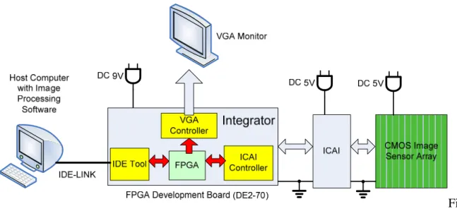
The study proposes a practical system used for remote sensing application with multiple CMOS image sensors. The system could integrate 4 strip CMOS image sensor, an ICAI (image combiner and acquisition interface) chip, a FPGA development board and a host computer to build a high-resolution multiple-aspect two-dimensional image. To form a high-resolution image, these strip CMOS image sensors are arranged in an interleaved form to avoid the spatial discontinuity. Thus, ICAI chip is used to control image sensors and to restore an interleaved image to an original image. The below chapter would explain an interleaved image. The FPGA development board connects ICAI chip to compose real-time image files and also keeps the communication with a host computer. The FPGA development board is an integrator for all peripherals and it is a key hardware of the system.
The host computer is as the server in satellite transmission stations in earth. The host computer could process raw image files and save as long-term data. Because there are some problems in satellites’ raw image files, the image post-processing software in the host computer is viewed as a key component of the system. Hence, the study focuses on design of the two parts: one is the design of image post-processing software and the other is the design of interface hardware by FPGA development board.
1.2 Component and Platform
1.2.1 System Block Diagram
The embedded system mainly includes CMOS image sensors more than one, an interface chip and a FPGA development board with peripherals. The interface chip is named as ‘image combiner and acquisition interface’ or ‘ICAI’. ICAI processes the data from multiple CMOS image sensors and is integrated with the FPGA development board. The FPGA development board is the integrator for all components by hardware solutions and the communicator with the host computer. For example, FPGA development board must implement ICAI controller and VGA controller to drive the operation of ICAI and VGA chip. By the way, a VGA monitor could display image in real-time from VGA port on FPGA development board.
IDE-Link is like the link between a satellite and a server in satellite transmission station. IDE-Link is built in Nios II IDE (Integrated Development Environment) and provides a simple method for downloading data from the FPGA development board to the host computer. The hardware of IDE–Link is with JTAG interface that is normally for debug. Besides, the host computer is the receiver of image data.
3
To demonstrate the imagery system, the study designs a prototype to approach the concept. The architecture of the system is shown as Figure 3. In below articles, these components are introduced in detail.
Fi gure 3: System block diagram
1.2.2 Sensor
The system use CMOS image sensors to capture image and the size of one sensor is 704 pixel × 1 pixel. The geometry about the strip sensor is 6.5um × 1500um. It means that the sensor is a one-dimension structure. To get a full image in the space, the sensor constructs a two-dimensional image by scanning in spatial domain. The full image size is determined by scan steps and the scan rate must match the satellite speed. These strip sensors are aligned as a ‘liner’ sensor, the resolution becomes (several times of 704) pixel × 1 pixel. After package, the image sensor array is like an interleaved structure and there are overlap areas between neighboring sensors. The practical alignment is shown in Figure 5.
4
1.2.3 ICAI
The other important part of the system is ICAI chip to capture the image of the sensor array. ICAI is a programmable interface between CMOS image sensor chip and host computer. There are three blocks in the ICAI – CIS control logic, CIS image combiner and host interface. The CIS control logic activate CMOS image sensor and acquire image data periodically. The one-dimension image is combined to form a two-dimension image by the CIS image combiner. The host interface receives and parses commands from the host computer. In addition, the host interface wraps the processed image data, and then transmits back to host computer for further image processing. The architecture of ICAI is shown in Figure 5. Due to the CMOS image sensor space arrangement, the image data should be rearranged by CIS image combiner. The process flow of combining image is as Figure 6. The symbols, A, B, C and D, represent the image from four CMOS image sensor. The suffix in these symbols means their acquisition time index. Due to the acquisition timing, A1, B1, C1 and D1 will be acquired by ICAI at the same time. However, A1, B2, C1 and D2 should be the same line.
Figure 5: ICAI architecture
A1 B2 C1 D2 B1 D1 A2 B3 C2 D3 A3 B4 C3 D4 A C B D A4 C3 1D CIS Image 2D CIS Interleaved Image A1 B2 C1 D2 B1 D1 A2 B3 C2 D3 A3 B4 C3 D4 A4 C3 2D CIS Image To FPGA Board CIS Domain ICAI Domain
Figure 6: Process flow of combining image
1.2.4 Integrator by FPGA Development Board
In the embedded system, the integrator is FPGA development board. The integrator responds for gathering data from ICAI, transferring image data to VGA monitor in real time and saving image file to host computer. To achieve the functions, the necessary peripherals include VGA port and GPIO port. The VGA port is for image displaying and the GPIO port is used for ICAI controller. We choose the Altera DE2-70 development board to build the image system.
The DE2-70 use Altera Cyclone II 2C70 FPGA as the core chip, and the core chip characteristics: 68,416 LEs (Logic Element), 250 M4K RAM blocks, 1,152,000 total RAM bits, 150 embedded multipliers, 4 PLLs, 622 user I/O pins, and FineLine BGA 896-pin package. The photograph of DE2-70 is shown in Figure 7. The block diagram of DE2-70 is shown in Figure 8.
Figure 7: Photograph of DE2-70
Figure 8: Block diagram of DE2-70
7
1.2.5 Host Computer and Image Post-Processing Software
In the overall system, it includes a host computer that is as server in earth. The software on the host computer responds for image post-processing and these image raw data are from the FPGA board. The OS (operation system) of the host computer is
Microsoft Windows.
The host computer must process the raw bitmap to approach the real image. ‘Real’ means that it must eliminate some variation from hardware parts, ex. difference among sensor chips, package mismatch, etc. The other special function is HD Photo conversion. HD Photo is a better image compressible format than JPEG. The higher compressible rate is efficient in space application. In conclusion, the software has two main functions: eliminating hardware variation and HD photo encoding.
1.2.6 Sensor Emulator
To implement the system rapidly, we use the sensor emulator to take a trial-rum. The sensor emulator is also designed by using DE2-70 development platform. First of all, pattern image, which has resolution of 704 × 704 pixels, has been extended sixteen times to store in the memory of sensor emulator. Because there is only 65,536 bytes in the memory, the pattern image (704 × 704 pixels) is stored in 1 bit per pixel format. Due to the output bandwidth, two dual-port memories are utilized for storing pattern image. Each dual-port memory has two output port and two address port. The configuration of memory block is shown in Figure 9. Every line is formed by 88 bytes, that is, 704 (88 × 8) pixels per line. However, each line is split equal and stored in two dual-port memories. Because the data is programmed into the sensor emulator while programming FPGA, there is no need to write any data to the memory during emulation.
The control logic in sensor emulator read out pattern image in sequence. However, every pixel and every column are repeated four times. A simple interpolation technique is applied to extend 704 × 704 pixels to 2816 × 2816 pixels. The concept is depicted in Figure .
Figure 9: The configuration of two dual-port memory. 704 colum ns (lines) 704 pixels 704 4 pixels 704 colum ns (lines)
(a) CIS Image sensor (b) CIS Image sensor
Figure 10: The applied interpolation concept in sensor emulator
Chapter 2 Hardware Architecture
2.1 Hardware Architecture of FPGA Board
The hardware architecture consist two parts: one is image capture unit with ICAI and the other is displaying image in real time. These parts mainly are implemented by VHDL codes and they are several parts: Nios II CPU kernel, ICAI controller, VGA controller, multi-port SDRAM controller and PLL.
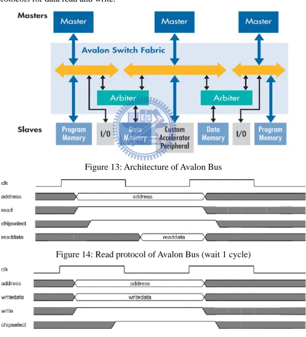
Briefly mentioning the FPGA architecture, Nios II CPU kernel is the main controller and arbiter for all procedures on the FPGA board. ICAI controller is a driver to ICAI chip and its protocol must follow ICAI definition explicitly. ICAI controller use 40-pin GPIO to connect. VGA controller is used to display real-time image on VGA-compatible monitor. Multi-port SDRAM controller is a frame buffer to process data between ICAI controller and VGA controller. Almost all components should be linked with a bus that is named as ‘Avalon Bus’. The components on Avalon Bus must be either ‘Master’ or ‘Slave’.
Besides the FPGA architecture, there are some peripheral chips on the FPGA development board. The VGA chip is a 10-bit video DAC (digital to analog converter) and its output corresponds to VGA protocol with D-sub connector. The SRAM and SDRAM are on-board memory supported as buffers or CPU caches. In additional, IDE-Link could respond for dumping data from DE2-70. PLL generates two clocks with different frequency: 8MHz and 16MHz. 16MHz is for the sensor emulator and 8MHz is for ICAI. The system block diagram of the integrator is shown in Figure 11.
10
The hardware development environment is Altera Quartus II, and Quartus II has some powerful additional tool. SOPC (System On Programmable Chip) Builder is used to set Nios II CPU characteristics and the relation between CPU and peripherals in Avalon Bus structure. After finishing SOPC setting, Quartus II would transfer the
settings to VHDL codes besides some licensed IP. Users could freely use these VHDL codes in hardware system. Quartus II also provides simulation and synthesis functions to implement hardware design on Alter FPGAs.
Figure 11: System block of Integrator by FPGA board
2.2 Nios II CPU
Nios II is Alter ‘s second generation Soft-Core 32-bit RISC Microprocessor. It could be targeted and programmable for Altera FPGA. Nios II is normally built by SOPC Builder. Therefore the synthesis of Nios II also uses Quartus II Integrated Synthesis. Because using Quartus II to implement Nios II, the other peripherals could be easily integrated together.
In SOPC Builder environment, users could integrate NIOS II CPU, memory interface, peripheral interface, Ethernet port and so on, even additional IP to a single FPGA chip. The Soft-Core is programmable, so CPU specification is flexible and easily to modify. The advantage of FPGA design flow is a trade-off among cost, performance and development complexity. Figure 12 shows block diagram of NIOS II
Soft-Core. Program Controller & Address Generation Instruction Cache clock reset irq[31..0] Control Registers ctl0 to ctl4 Arithmetic Logic Unit Hardware-Assisted Debug Module Interrupt Controller JTAG interface to Software Debugger Custom Instruction Logic Exception Controller Instruction Bus Data Cache Data Bus General Purpose Registers r0 to r31 Custom I/O Signals
Nios II Processor Core
Tightly-Coupled Instruction Mem Tightly-Coupled Instruction Mem Tightly-Coupled Data Mem Tightly-Coupled Data Mem
Figure 12: Block diagram of NIOS II Soft-Core
2.3 Avalon Bus
Nios II use Avalon Bus as general buses in its applications and it means that Avalon Bus is the interconnect between CPU and other peripherals. Avalon Bus defines the relation between master and slave. Avalon Bus also provides arbitration function to control the priorities of components. The features of Avalon Bus include:
1. Clock synchronization: Avalon Clock controls all signals on Avalon Bus and there are no handshaking and no acknowledge. The synchronization mechanism could increase the transfer speed.
2. Variable data widths: On Avalon Bus, the data width could be set as 8-bit, 16-bit or 32-bit.
3. Arbitration technology: If many components have transfer requests on Avalon Bus in the same time, CPU would automatically take arbitration to schedule all requests.
12
signals are independently assigned. The assignments are simple for interface design with the standard naming rules.
5. Memory-Mapped technology: CPU control peripherals by the addresses that are generated by Memory-Mapped. Memory-Mapped is automatically or manually executed in SOPC Builder.
Figure 13 shows the architecture of Avalon Bus. Figure 14 and 15 show simple protocols for data read and write.
Figure 13: Architecture of Avalon Bus
Figure 14: Read protocol of Avalon Bus (wait 1 cycle)
Figure 15: Write protocol of Avalon Bus (no wait)
2.4 VGA controller
VGA controller is like the driver to the high speed video chip on FPGA board. The high speed video chip is triple 10-bit in RGB and its max resolution is 1600 × 1200 at 100 Hz refresh rate. VGA controller could be set resolution and refresh rate. The default value is 800 × 600 at 60 Hz refresh rate. The architecture of VGA controller is shown in Figure 16. VGA CLK and triple 10-bit RGB data would be sent to VGA controller and the controller would generate Read EN to enable the high speed video chip. In the other hands, VGA controller would send HSYNC, VSYNC, Red, Green and Blue signals that are corresponding for VGA protocol timing.
Figure 16: Architecture of VGA controller
2.5 ICAI controller
2.5.1 ICAI Protocol
14
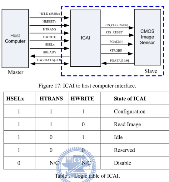
The ICAI to host computer interface is shown in Figure 17. The signal of “HSELx” enables ICAI. The signal of “HWRITE” and “HTRANS” define the states of ICAI. The logic table is listed in Table . The signal of “HCLK” and “HRESETn” provides the clock and reset signal for ICAI respectively. The bus of “HRWDATA” is used to transfer data in and out of ICAI. The signal of “HREADY” indicates if the value on the “HWRDATA” bus is valid.
Figure 17: ICAI to host computer interface.
HSELx HTRANS HWRITE State of ICAI
1 1 1 Configuration
1 1 0 Read Image
1 0 1 Idle 1 0 0 Reserved
0 N/C N/C Disable
Table 1: Logic table of ICAI.
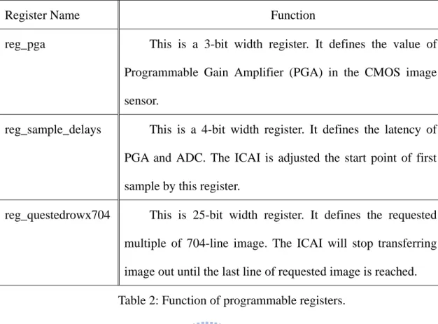
The timing diagram of configuring ICAI is shown in Figure 18. The ICAI should be programmed before reading image from the CMOS image sensor. A total of 3 registers can be programmable – ‘reg_pga’, ‘reg_sample_delays’ and ‘reg_questedrowx704’. The functions of these registers are described in Table .
reg_pga reg_sample _delays 1T=125ns
Figure 18: Timing Diagram of configuring ICAI.
Register Name Function
reg_pga This is a 3-bit width register. It defines the value of Programmable Gain Amplifier (PGA) in the CMOS image sensor.
reg_sample_delays This is a 4-bit width register. It defines the latency of PGA and ADC. The ICAI is adjusted the start point of first sample by this register.
reg_questedrowx704 This is 25-bit width register. It defines the requested multiple of 704-line image. The ICAI will stop transferring image out until the last line of requested image is reached. Table 2: Function of programmable registers.
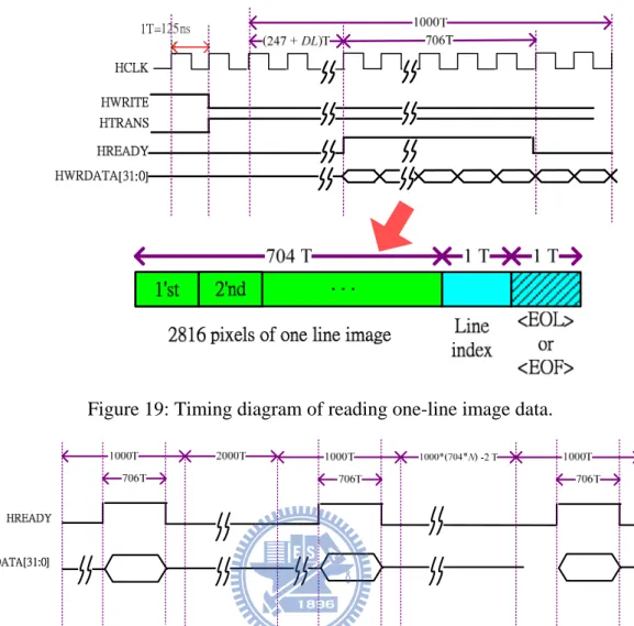
The timing diagram of reading one-line image data is shown in Figure . The ICAI will output image data in the read image state every 1000 clock cycles until the last line of requested image is reached. The value of ‘reg_sample_delays’ is denoted by variable K in Figure . Although the image data is outputted every 1000 clock cycles, only 706 clock cycles are occupied. The output packet includes 2816 pixels image data, the value of line index and the symbols of “End of Line” or “End of File”. The symbol of “End of File” will only be outputted when the last line of requested image is reached. A timing diagram of reading full 2D image is shown in Figure . Note that the ICAI will response the configuration value in first 1000-cycle duration. In the following two 1000-cycle duration, the ICAI will not output any image data because there are 3000 clock cycles latencies for ICAI. The value of “reg_questedrowx704” is denoted by variable N in Figure .
Figure 19: Timing diagram of reading one-line image data.
Figure 20: Timing diagram of reading full 2D image.
2.5.2 ICAI Controller Architecture
The architecture of ICAI controller includes ICAI controller logic block, control registers and FIFO RAM. ICAI controller logic block is a generator to send ICAI control signals, like HRSET, HTRANS, etc. The control registers are saving the necessary logic table. The FIFO RAM provides the buffer to multi-port SDRAM controller. The Avalon Slave is the interface to CPU with Avalon Bus. The architecture of ICAI controller is shown in Figure 21.
Figure 21: Architecture of ICAI controller
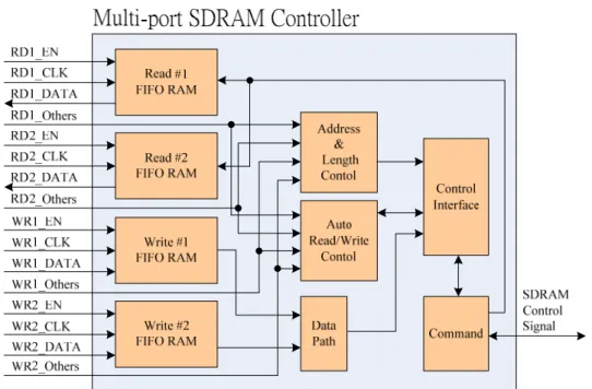
2.6 Multi-Port SDRAM Controller
The multi-port SDRAM controller is a 2-port write and 2-port read memory controller. One write port is connected to ICAI controller and one read port is connected to VGA controller. The other read port and write port are for CPU to access SDRAM. The main function of the block is providing the high speed buffer to VGA controller. The SDRAM control signal is a ‘start’ pulse to set the controller. The multi-port SDRAM controller block diagram is shown in Figure 22.
Figure 22: Architecture of multi-port SDRAM controller
Chapter 3 Software Architecture
3.1 Software Platform
3.1.1 GUI Software
Because the image post-processing software on computer focus on processing the bitmap files from the embedded system, Microsoft Visual Studio 2008 is chosen to develop the GUI (Graphic User Interface) software. In MFC (Microsoft Foundation Class) libraries built in Microsoft Visual Studio, GDI (Graphics Device Interface) class is suitable for processing bitmap files. By GDI class, we could quickly load bitmap, save bitmap, or gather image information like height or width. In addition, using Microsoft Visual Studio 2008, building GUI software becomes convenient.
3.1.2 HD Photo Software Development
HD Photo format is provided and developed by Microsoft and it releases the comprehensive source codes. The sources codes are firstly designed for Console Application (like DOS) in Microsoft Visual Studio 2005. In order to integrating conversion to HD Photo in the software, development by Microsoft Visual Studio 2008 is easily compatible.
3.1.3 Software Flow
The bitmap of the embedded system is captured by 4 CMOS image sensors. The object of the image post-processing software is processing some difference among multiple sensors. Therefore, the software has four main functions: image gray-level shifting, package offset cancellation, image overlap cancellation and HD photo encoding.
19
Normally, the four main functions could be used in sequence. Firstly, image gray-level shifting applies an original image into a calibrated image. Secondly,
package offset cancellation and overlap cancellation should modify the mismatch of sensors package. After modification, the finished image is also saved as the other bitmap file.
If it is necessary to convert bitmap to HD photo file, HD Photo encoding could complete the work finally. Figure 23 is the software flow chart to describe the above steps.
Figure 23: Software flow chart
For easily explaining the software function, we define the two-dimension image as X-axis and Y-axis directions. The X-axis direction is perpendicular to sensors and the Y-axis direction is parallel with sensors, and a simple figure is shown in Figure 3.
3.2 Problems in the Sensor Array
The embedded system has multiple sensors and these sensors should be arranged as one interleaved line by package process. The package process includes bonding and alignment. Because the sensors are with strip-type, the alignment process becomes
difficult. There are some problems occurred in alignment process. One is the sensors package offset in X-axis direction. In ICAI design concept, it could modify the interleaved image and it assumes that package offset is ‘one’ pixel. But in real application, package offset may be not one pixel, even non-integer pixel. The software must be used to adjust the package offset.
The other problem in package is overlap areas among sensors in Y-axis direction. In concept of alignment, the overlap area should be reserved between neighboring sensors, so that it is no gap between neighboring sensors. A sensor array without any gap could be viewed as a ‘continuous’ liner sensor. Because ICAI captures all data from multiple sensors for all pixels, the image has some repeating areas in borders of neighboring sensors. There must be some overlap areas between neighboring sensors from ICAI image raw data. The Figure 24 shows an embodied graph of two problems.
X-Axis
Figure 24: Sketch graph of package offset and overlap
The other problem in package is that sensors are aligned obliquely referring to the X-axis. The angle of oblique is relative with the precision of package process. Because the size of a sensors is 6.5um (width) × 1500um (height), the oblique angle would make a sensor shifting. For example, shifting 0.115∘would make the image shifting 1
pixel. But, the angle in the software is hard to define implicitly and we define the shifting pixel in the software. The sketch graph of oblique alignment is shown in Figure 25.
A B C D
Scanning Direction
Y-Axis
A,B,C,D are strip CIS
Oblique Alignment
Figure 25: Sketch graph of oblique alignment
The final problem is gray-level variation for pixels. Because the optical devices are used in front of sensors in light path, the vignetting effect would be occurred. Because the systems use strip-type sensors to scan a full image, the vignetting makes the image with gradient gray-level. The normal picture with vignetting effect is shown in Figure 26. Because the system uses 4 strip sensors, the scanned image with vignetting effect would be divided 4 strip regions. The sketch image for scanning a fully white image is shown in Figure 27.
Figure 26: Vignetting effect in corners of photograph
Figure 27: Vignetting effect for scanning a fully white image by the sensor array In order to compensate these problems in sensor array, the calibration becomes a critical procedure and by the procedure we could get parameters in package process. In summary, we must do calibration after package process by 4 steps:
1. Calibration for package offset. 2. Calibration for overlap
3. Calibration for oblique alignment 4. Calibration for gray-level variation
3.3 Calibration Method after Sensors Package
3.3.1 Calibration Flow
From the above discussion, the calibration after package is significant for the system. There must be a list of calibration parameters for each package. If package process is reworked, the calibration parameters must be collected again. These parameters would be loaded into the software, so different packages have different lists of calibration parameters. The flow for the calibration is shown in Figure 28.
Figure 28: Calibration flow for sensor array
3.3.2 Calibration for Gray-Level Variation
24
To calibrate the vignetting effect form optical devices, we choose to gather data from a fully white image and a fully black image in real application. For ideal sensor, a fully white image makes gray-levels of all pixels become 255 in 8-bit resolution, and on the contrary a fully black image makes these values become 0. In real application, the gray-levels in a fully white image and a fully black image would be not 255 and 0, and we use linear transform for mapping real values. The ideal and real gray-level
mapping are sketched in Figure 29. The formula of linear transform is shown in Figure 30. By the step in Figure 30, the lists of calibration parameters must store 2 parameters for all pixels, and the 2 parameters are ‘a’ and ‘b’ in Figure 30.
Figure 29: Ideal and real gray-level mapping
b
ax
x
f
(
)
=
+
n
m
m
b
m
n
a
n
f
m
f
−
=
−
=
⇒
=
=
0
,
(
)
255
255
,
255
)
(
Figure 30: linear transform between ideal and real gray-level mapping
3.3.3 Calibration for Package Offset and Overlap
25
The package offset and overlap would lead to geometry mismatch. Thus, we choose 2 special pictures to correct them. For package offset, we use a drawing with various gaps and it is shown in Figure 31. The gap varies from 6.5um to 130um to cover all ranges of package offset and the gap size is a multiple of the sensor width.
After capturing the picture by the sensor array, we could check the position of ‘nearly’ continuous line, and the ‘nearly’ continuous line means that the original gap is compensated. The package offset value is the value of gaps in the position. After the steps, the list of parameter must store a parameter for each sensor.
For finding the size of overlap area, we choose a picture with a fixed width like Figure 32. The widths of black and white region are both 1500um that equals to the sensor height. After capturing the picture by the sensor array, we could check the length of black and white regions. Even if shifting in scanning process, by the simple calculation, the overlap area of each sensor could be obtained.
6.5um*2 6.5um 6.5um*3 6.5um*18 6.5um*19 6.5um*20 1800um 6.5um
Sensor A Sensor B Sensor C Sensor D
Figure 31: Calibrated drawing with various gaps neighboring between sensors
Figure 32: Calibrated drawing with fixed black and white regions
3.3.4 Calibration for Oblique Alignment
Finally for oblique alignment, we choose a picture with a fixed rectangular black region as the calibration image and shown in Figure 33.
Figure 33: Calibrated drawing with rectangular black regions
In the calibration, we do not find the oblique angle of alignment, and we want to obtain the shifting value for each pixel. For example, if the oblique angle is below
0.115∘, the shifting values are 0 for all pixels; on the contrary if the oblique angle is about 0.23∘, the shifting values are 1 for some pixels. If the sensors are obliquely aligned, the image by scanning the rectangular black region would be distorted like Figure 34. From Figure 34, we could check the shifting value by borders and build the lists of calibrated parameters for each pixel.
Figure 34: Calibrated drawing with oblique alignment (The oblique alignment is like Figure 25.)
3.4 Gray-Level Shifting
3.4.1 Gray-Level Difference among Sensors
Because the system uses multiple sensors, there must be some variation among sensors in wafer process that leads to different sensors characteristics. Because the sensors have only 8-bit gray-level, the software has a simple solution to calibrate the difference among sensors.
3.4.2 Gray-Level Shifting Function
From the structure of the sensor array, originally there is an overlap area between neighboring sensors. The overlap area provides a reliable reference to calibrate two images.
Theoretically, the overlap area of two sensors should have the same characteristics. If there is any difference by comparing overlap area of two images, the two image should be corrected based on one of them.
In concept, we calculate the gray-level averages of overlap areas for neighboring two sensors. Next we calculate the variation between the two sensors. Finally we take the image of one sensor to substrate the variation, and the two images of two sensors should be nearly matching. The step and formula is show in Figure 35.
Height Width G G Width height * 1 1
∑ ∑
= Height Width G G Width height * 2 2∑ ∑
= 2 1 G G G= − Δ G G G2′= 2−ΔFigure 35: Step and formula of gray level shifting
3.5 Image Overlap Cancellation
3.5.1 Image Overlap from the Sensor Arrangement
In package process, the image overlap area between neighboring sensors is not fixed and the software must dynamically process to cancel the error. The software must dynamically process to cancel the overlap areas. In practice, the value of overlap area
is about 1~10 pixels. Because the overlap area must exist in the system and the function must be executed in image post-processing.
3.5.2 Image Overlap Function
The software design the overlap cancellation function for 4 image sensors, and the image height must match the ICAI output data format. Therefore the image height is set as 704 pixels. Explaining the function by step:
1. Fix the image of the first sensor.
2. Move the effective area of the second sensor to adjoin the image of the first sensor. It means that cut the overlap area of the second sensor.
3. The same method is like step 2. It processes the image of the third sensors to adjoin the image of the second sensor.
4. The same method is like step 2. It processes the image of the forth sensors to adjoin the image of the third sensor.
The brief diagram is shown in Figure 36.
30 Scanning Direction Y-Axis Overlap Areas A1 C2 A4 A3 A2 B2 D1 D2 D3 B3 B4 C1 C3 C4 Y-Axis A1 C2 A4 A3 A2 B2 D2 B1 D4 After Processing 1st Fixed C1 B1 D1 C3 B3 D3 C4 B4 2nd Fixed 3rd Fixed D4
3.6 Package Offset Cancellation
3.6.1 Package Offset from the Sensor Arrangement
Like the problem about overlap cancellation, the package offset between neighboring sensors is not fixed and the software must dynamically process to cancel the error. In practice, the value of package offset is about 0~10 pixels and the offset may be right or left. If there is no offset after package, the function could not be executed or set as zero offset.
3.6.2 Package Offset Cancellation Function
The software design the package offset cancellation function for 4 image sensors, and the image height must match the ICAI output data format. Therefore the image height is set as 704 pixels. Explaining the function by step:
1. Fix the image of the first sensor.
2. Move the image of the second sensor to match the image of the first sensor. We define ‘Move Left’ as ‘negative’ direction and ‘Move Right’ as ‘positive’ direction.
3. Move the image of the third and forth sensor to match the image of the first sensor. The offset value is defined in base of the first sensor.
The brief diagram is shown in Figure 37.
Figure 37: Graph of package offset cancellation function
3.7 HD Photo File Conversion
3.7.1 Introduction to HD Photo
HD Photo is a file format and associated codec specifically designed to for use with all types of still image. HD Photo is released by Microsoft Corporation firstly, and its browser is built in Windows Vista, Windows Presentation Foundation (WPF) and Windows Imaging Component (WIC). In addition, Adobe Photoshop also supports to access HD Photo by plug-in files from Microsoft. The main features of HD Photo are listed below.
1. It uses a friendly compression method with simple integer-only operation and then it needs small memory buffer.
2. The compression quality is industry-leading similar with JPEG2000. 3. It supports a very wide range of pixel format, especially in high BPP (Bit
Per Pixel) format.
4. It uses the same algorithm for lossless and lossy compression.
Regarding the former image formats, HD Photo supports high BPP format to elevate performance in color space. The wider color space is named as ‘scRGB’ that is developed by Microsoft. scRGB color space supports 16-bit BPC (Bit Per Color) even 32-bit BPC, and the specification of 16-bit BPC corresponds features of almost digital image products. scRGB color space also covers HVS (Human Visual System) color space and overcomes poor performance of sRGB color space that is only 8-bit BPC. In the satellite remote sensing system, HD Photo has some advantages. By using scRGB color space, the image sensors could be designed for high bit and high sensitivity. The scRGB color space is show in Figure 38.
Figure 38: scRGB color space
3.7.2 HD Photo Encoding Process
HD Photo encoding process is based on ‘Photo Core Transform’ that is called as PCT. It is similar with DCT (Discrete Cosine Transform) used in JPEG, and it still has a special compression algorithm. The encoding process of HD Photo is show in Figure 39.
PCT is core mapping of the process. The three elements of PCT are Hadamard transform, 1-D rotation transform and 2-D rotation transform. The codes of the three
transforms are list in Table 3. Table 3 shows that only integer operations and bit shifting are used in PCT. On the contrary, DCT must have floating-point operation.
Figure 39: Encoding process of HD Photo
Table 3: (I) Hadamard transform, (II) one-dimension rotation transform and (III) two-dimension rotation transform
3.7.3 Comparison among HD Photo, JPEG, JPEG2000
From reference, Table 4 shows performance of three image format. Table 5 shows the feature comparison of HD Photo, JPEG and JPEG2000. The performance of HD
Photo and JPEG2000 are nearly the same. The two image formats are with latest technology and better than JPEG. The supporting functions from Table 5 of the two image format are powerful. Therefore, the advantages of HD Photo should be low complexity.
PSNR Bit Rate
HD Photo JPEG JPEG2000
4 BPP 45.95 41.56 44.65
2 BPP 39.81 34.58 38.26
1 BPP 34.46 32.41 33.17
Note: BPP: Bit Per Pixel; PSNR: Peak to Signal Noise Ratio
Table 4: Performance of HD Photo, JPEG, JPEG2000 [1]
HD Photo JPEG JPEG2000
Integer operation Y N N
Space scalability Y N Y Operation without decoding Y N Y
ROI encoding N N Y
ROI decoding Y N Y
Large picture Y N Y
N-channel color format Y N Y Row by row encoding N N Y Separable transformation N Y Y Table 5: Features and Functions of HD Photo, JPEG, JPEG2000 [1]
3.7.4 HD Photo Encoder Function
35
The source codes of HD Photo encoder/decoder are release from Microsoft. The source codes provide many controllable parameters to set HD Photo characteristics.
The more important parameters are shown in Table6. The software must include the parameters in Table 6 for conversion setting.
Item Parameter Note
Compression Quality 1~255 1: Lossless (Default) 255: Max. Compression Source Pixel Format 0~34 0: 24bppBGR (Default)
1: BlackWhite 2: 8bbpGray
………… Overlapping Level 0~2 0: no overlapping
1: 1 level overlapping (Default) 2: 2 level overlapping Input File Name (*.bmp) xxx opened file name Output File Name (*.wdp) xxx any name
Table 6: Main parameters of HD Photo encoder
The software directly uses the complied file to encode bitmap files. The GUI includes 3 columns to choose the 3 main parameters and 2 columns to set filenames. After press ‘OK’ button, the execution file would encode the bitmap file to HD Photo file. The operation runs in background and the HD Photo file is saved in the same directory.
Chapter 4 Experimental and Testing Results
4.1 Hardware Experimental Result
4.1.1 Hardware Simulation
The hardware simulation focuses on ICAI controller operation. The simulation tool is ModelSim that is built in Altera Quartus II.
In starting ICAI chip, the system would send a ‘Start’ signal to ICAI controller. After receiving the ‘Start’, the behavior of ICAI controller must send the signals like protocol. Firstly, we check the signals: HSELx, HTRANS, HWRITE, HRESETn and registers to configure ICAI. The first simulation result is shown in Figure 40. From Figure 40, we could check the configuration status of ICAI (red circle marked). After resetting the system (Reset_n is from 0 to 1) and then starting ICAI by keeping HSELx as 1, HTRANS and HWRITE would both become high level with one CLK latency. At the same time, L_DATAO would send 32-bit data to registers to configure ICAI. The example also shows a 32-bit register value.
Figure 40: First simulation result of ICAI controller
37
Second, we could check the start point of ICAI data. The design specification is (247+DL) CLK like Figure 18. ‘DL’ is set as 0 in the register and then the start point is correct. The iTransmitCount is counting from HTRANS and there is one clock delay.
Figure 41 shows the simulation result.
Figure 41: Second simulation result of ICAI controller
4.1.2 Hardware Experiment
Because we use sensor emulator as image source, ICAI would capture image from 4 ‘virtual’ sensors. Because ICAI design is for the interleaved image and the sensor emulator could not store the interleaved data, the final image captured by ICAI is an interleaved image. The final bitmap is shown in Figure 42 and the zoom-in bitmap is shown in Figure 43. The discontinuity is due to the interleaved effect.
Figure 42: Image captured by ICAI
Figure 43: Zoom-in of image captured by ICAI (5 red marked regions)
4.2 Software Operation
4.2.1 Introduction for Software GUI
The GUI of the image post-processing software is shown in Figure 44. The basic functions that are like ‘Open File’, ‘Save File’, etc are built by MFC wizards. The ‘Main Functions’ include 4 functions described in Chapter 3. The 4 functions are introduced in detail.
39
Using ‘Gray-Level Shifting’ could compensate the variation among sensors and the overlap areas should be referred. After opening the function, the ‘Dialog’ box shows 3 columns. The 3 columns must be filled the parameters of second, third and forth sensors. These parameters in the function mean the overlap pixels between neighboring sensors. For example, the second column is the setting for third sensors and the value in the column is the overlap pixels between the second sensor and the third one. The dialog box of ‘Gray-Level Shifting’ is shown in Figure 45. The function should modify gray levels of the second, third and forth sensors to match the first
sensor.
Figure 44: Main window
Figure 45: Main dialog box
Next, using ‘Overlap Cancellation’ function could compensate the package overlap areas among sensors. After opening the function, the ‘Dialog’ box shows 3 columns and the 3 columns must be filled the overlap pixels between neighboring sensors. The parameters of ‘Overlap Cancellation’ normally should be the same with
the ones of ‘Gray-Level Shifting’ function. The method of correction is that fixing first sensor’s position and moving the second, third and forth sensors step by step. Therefore, the ‘Overlap Cancellation’ function would make the bottom of image with some blanking pixels. The bottom blanking are filled a fixed gray-level value.
Next, using ‘Package Offset Cancellation’ function could compensate the package error among sensors. After opening the function, the ‘Dialog’ box shows 3 columns like ‘Gray-Level Shifting’ function and the 3 columns must be filled the pixel value of package offset. The values are referred to first sensor, so the second, third and forth sensors should be corrected to match first sensor’s position after operation. The ‘Package Offset Cancellation’ function would make the image with some blanking pixels, these pixels of blanking area are filled a fixed gray-level value, too.
Finally, ‘HD Photo Function’ provides the conversion to HD Photo in the same GUI. Because the function calls the sub-program that runs in command mode, the bitmap file must be saved in the same directory with the sub-program. After the bitmap file is updated, the function could process the latest bitmap file. The GUI provides 3 parameters to control HD Photo format. ‘Quality’ is limited from 1 to 255, ‘Format’ is limited from 0 to 34 and ‘Overlapping’ is limited from 0 to 2. The input and output filenames are limited 32-bit length. The dialog box is shown in Figure 46.
41
4.3 Software Test
4.3.1 ‘Gray-Level Shifting’ Function Test
To test these functions of software, the standard bitmap ‘lena.bmp’ would be used. The specification of lena.bmp is 256 pixel × 256 pixel and 256 gray level. The one sensors area is defined as 256 pixel × 64 pixel and totally there must be 4 sensors to construct a full image. To try these functions, a faked lena.bmp is created by normal image processing software on PC. The faked image spec is 256 pixel × 276 pixel and 256 gray level and the faked image has some artificial errors. The sensor effective area is also 256 pixel × 64 pixel, so the software must correct the faked image. In real application we just modify the specification of sensor pixel from 64 pixel to 704 pixel in source code, and then the software could be used in the system. The original image and the faked image is shown inFigure 47.
Figure 47: lena.bmp and lena_faked.bmp
The software loads the faked image and the faked image shows 4 regions with different gray-level distributions. After executing the ‘Gray-Level Shifting’ function, the software would process the gray-level balance of the faked image. The effect of the
function is shown in Figure 48. Comparing with the original image, there is a little difference and the effect is acceptable.
Figure 48: lena_faked.bmp after Gray-Level Shifting
4.3.2 ‘Overlap Cancellation’ Function Test
The operation of ‘Overlap Cancellation’ is simple. The effect of the function is to modify vertical position of 4 sensors. The faked image is created with a little overlap region among sensors in vertical direction and the mismatch size is about 5~10 pixels. After executing the function, we could check the image is continuous as the original image. The effect of the ‘Overlap Cancellation’ is shown in Figure 49.
4.3.3 ‘Package Offset Cancellation’ Function Test
The operation of ‘Package Offset Cancellation’ is similar with the one of ‘Overlap Cancellation’. The effect of the function is to modify horizontal position of 4 sensors. The faked image is created with a little mismatch region among sensors in horizontal direction and the mismatch size is about 1~5 pixels. After executing the function, we could check the image is continuous as the original image. The effect of the ‘Package Offset Cancellation’ is shown in Figure 50.
Figure 49: lena_faked.bmp after Overlap Cancellation
Figure 50: lena_faked.bmp after Package Offset Cancellation
After the faked image is processed by the above 2 functions, the image in geometry is the same with the original image. We could zoom in the processed image and check the borders between neighboring sensors. The result of zoom-in is shown is Figure 51.
Figure 51: Zoom-in of processed lena_faked.bmp
4.3.4 ‘Convert to HD Photo File’ Function Test
The operation ‘Convert to HD Photo File’ function is filling 3 parameters and 2 filenames. The sub-program would run in background and generate *.wdp file. After processing the faked image by above 3 steps, we directly save the bitmap and then convert the processed image to HD Photo file. To check the HD Photo file if correct, we open the converted file in Microsoft Vista that supports to browse HD Photo file. The snap shot in Microsoft Vista is shown in Figure 52.
Figure 52: Display HD Photo file (*.wdp) in Vista
Chapter 5 Conclusion and Future Work
5.1 Conclusion
The study demonstrates an image recombination and processing system for one-dimensional multi-strip CMOS image sensors. The system could control the operation of CMOS image sensors by ICAI and provide the real-time ability to display and generate high resolution image. Its key hardware includes ICAI chip and the integrator on FPGA board. The integrator successfully connects ICAI and peripherals to display and to save image.
The other part in the study is image post-process software. The software solves the limitation and inconvenience of hardware. Especially, there are some package problems in practice, the software provides a simple method to restore the real image. The work of HD Photo is an additional advantage in the software. It provides a better image format for storage.
5.2 Future Work
For review the study, the system could add some hardware to improve the completeness. For example, it is better to add a link to host computer by RS232 or USB interface and to save image to SD card. The other aggressive idea is implementing HD Photo algorithm in the hardware and directly saving image as high compression rate file. The advantage is reducing communication load between satellites and satellite transmission stations.
Reference
[1] Yoshihiro Tsuruda*, Toshiya Hanada and Jozef van der Ha, “QSAT: A Low-Cost Design for 50kg Class Piggyback Satellite”, 26th ISTS, 2008-f-20, June 6, 2008. [2] Terasic Technolopy, “DE2-70 Development and Education Board User Manual”,
2007.
[3] Altera Corporation, “Embedded System Design Using FPGAs”, 2005. [4] Altera Corporation, “Embedded Design Handbook”.
[5] Altera Corporation, “Avalon Interface Specification”.
[6] Altera Corporation, “Nios II Software Developers’ Handbook”. [7] 蕭鴻森, http://www.cnblogs.com/oomusou/category/149442.html
[8] 廖裕評, 陸瑞強, “系統晶片設計-使用 Nios II”, 全華圖書. [9] 繆紹綱, “數位影像處理”, 普林斯頓國際股份有限公司. [10] 求是科技, “Visual C++數位影像處理大全”, 文魁資訊.
[11] D.D.Giusto and T Onali, ”Data Compression for Digital Photography: Performance comparison between proprirtary solution and standards”, IEEE International Conference on Consumer Electronics, Digest of Technical Papaers, 2007.
[12] Bill Crow, “HD Photo Implementation Guidelines”, Microsoft WinHEC 2007, 2007.
[13] Bill Crow, http://blogs.msdn.com/billcrow/default.aspx
[14] Microsoft Corporation, “HDPhoto_Feature_Spec_1.0”. [15] Microsoft Corporation, “HDPhoto_Bitstream_Spec_1.0”. [16] Microsoft Corporation, “HDPhoto_DPK_Spec_1.0_Edit”.
[17] 黃琪文, “具有 AHB 介面之 JPEG2000 編碼器系統設計”, 國立交通大學碩士 論文, 2003.