國 立 交 通 大 學
電信工程學系
博 士 論 文
利用金氧半場效電晶體, 鍺化矽電晶體, 和
磷化銦鎵/砷化鎵異質接面電晶體技術之射
頻吉伯特混波器及接收機系統架構
RF Gilbert Mixers and Receiver Architectures
Using CMOS, SiGe BiCMOS, and
GaInP/GaAs HBT Technologies
研究生:吳宗翰
指導教授:孟慶宗
鎵/砷化鎵異質接面電晶體技術之射頻吉伯特混波
器及接收機系統架構
RF Gilbert Mixers and Receiver Architectures Using
CMOS, SiGe BiCMOS, and GaInP/GaAs HBT
Technologies
研究生:吳宗翰
Student:
Tzung-Han
Wu
指導教授:孟慶宗 博士
Advisor: Dr. Chinchun Meng
國立交通大學
電信工程學系
博士論文
A Dissertation
Submitted to Institute of Communication Engineering
College of Electrical Engineering
National Chiao Tung University
in Partial Fulfillment of the Requirements
for the Degree of Doctor of Philosophy
in
Communication Engineering
Hsinchu, Taiwan
化銦鎵/砷化鎵異質接面電晶體技術之射頻吉伯
特混波器及接收機系統架構
學生:吳宗翰 指導教授:孟慶宗博士
國立交通大學
電信工程學系博士班
摘
要
本篇博士論文的研究主題包含新式高IIP
2吉伯特混波器架構、升
頻混波器、創新的鏡像抑制接收器架構及並串串並雙迴授寬頻放大
器。首先本論文中針對吉伯特混波器發明了更高性能的新架構,可使
對稱性大幅提升,進而使得在RF 頻率為 10-GHz時IIP
2的性能提升至
33 dBm。本文利用 2 um GaInP/GaAs HBT技術第一個完整地去比較
現有主動次諧波混頻器的優劣,並且實作出了一個
5.2-GHz次諧波混
波器,其
2LO-to-RF 隔絕度世界最高。在傳送機方面,利用 2 um
GaInP/GaAs HBT 及 0.35 um SiGe BiCMOS實作出結合微小化集總微
波分波器及LC電流鏡之高性能的升頻器。
接著,本論文實作出傳統的
Hartley 及 Weaver 鏡像抑制接收器,
外,本論文還提出了嶄新的
2.4/5.7-GHz 雙頻帶射頻接收機系統架
構,並且利用
0.18 um CMOS 及 0.35 um SiGe BiCMOS 加以驗證實作。
最後,本論文針對常用的並串串並雙迴授寬頻放大器提出了全新
的設計理論,並且經由
0.13 um CMOS 實驗結果加以驗證之。量測結
Using CMOS, SiGe BiCMOS, and GaInP/GaAs
HBT Technologies
Student: Tzung-Han Wu Advisor: Chinchun Meng
Department of Communication Engineering
National Chiao Tung University
Abstract
The research topics of this dissertation include novel high IIP
2Gilbert mixer topologies, active sub-harmonic mixers, up-conversion
mixers, novel image rejection receiver architectures, and the design
methodology of the shunt-series series-shunt double feedback wideband
amplifier.
Several mixer building blocks are demonstrated in this work. A novel
truly-phase-balanced sub-harmonic Gilbert mixer topology with high IIP
2is proposed. The sub-harmonic mixer exhibits 33 dBm IIP
2when the RF
frequency is 10-GHz. A high isolation 5.2-GHz stacked-LO Gilbert mixer
is demonstrated and the highest 2LO-to-RF isolation for the
direct-conversion architecture is achieved. In addition, up-conversion
mixers using the active/passive LC current mirrors and lumped rat-race
hybrids are demonstrated at 5-GHz by using GaInP/GaAs HBT and SiGe
HBT technologies. The design principles of the LC current mirror are
developed.
Next, a conventional SiGe HBT 47 dB image rejection Hartley
system and a GaInP/GaAs HBT 48 dB image rejection Weaver system are
demonstrated and analyzed. In addition, 2.4/5.7-GHz dual-band image
rejection architecture that combines the Weaver and Hartley systems is
proposed for the first time. The novel Weaver-Hartley down-converters
are demonstrated using 0.18 um CMOS and 0.35 um SiGe BiCMOS
technologies. A powerful diagrammatic explanation using the complex
and the secondary image signals of the Weaver architecture in this
dissertation.
Finally, a shunt-series series-shunt double feedback loops wideband
amplifier is demonstrated in 0.13 um CMOS technology. The design
formulas of the small signal S parameters are determined to design the
wideband amplifier. The experimental results highly agree with the
design equations.
Contents
Abstract (Chinese)……….i Abstract (English)………...iii Acknowledgement………v Contents………..………vii List of Tables………ix Figure Captions……….…………...x Chapter 1 Introduction…………..………1Chapter 2 High Performance Direct-Conversion Sub-Harmonic Gilbert Mixers……9
2.1 Conventional Sub-Harmonic Gilbert Mixers……….11
2.2 Novel Highly Symmetrical Sub-Harmonic Gilbert Mixer Using Compensated Stacked-LO Stage……….….31
Chapter 3 High Performance Up-Conversion Mixers Using the LC Current Mirror and the Lumped Rat-Race Hybrid………..…..45
3.1 SiGe HBT Up-Conversion Gilbert Mixer Using the LC current Mirror and the Lumped Rat-Race Hybrid………...…..45
3.2 GaInP/GaAs HBT Up-Conversion Mixer Using the LC Current Mirror and the Lumped Rat-Race Hybrid………...……66
3.3 SiGe Up-Conversion Mixer Using Active-Inductor LC Current Mirror……68
Chapter 4 Conventional Image Rejection Architectures……….…73
4.1 Hartley Image Rejection Architectures……….………….74
4.2 Weaver Image Rejection Architectures……….………….88
4.2a The Diagrammatic Explanation of the Image Rejection Degradation in Weaver Architecture……….………...…….91
4.2b Image Rejection Improvement of the Weaver Down-Converter…….94
4.2c Implementation of the GaInP/GaAs HBT Weaver System……….….98
Chapter 5 Dual-Band Down-Converter Using Weaver-Hartley Image-Rejection Architecture……….………...112
5.3 2.4/5.7 GHz Dual-Band Down-Converter Using 0.18 um CMOS Technology.
………..…..123
5.4 2.4/5.7 GHz Dual-Band Down-Converter Using 0.35 um SiGe BiCMOS Technology………..…..…..138
Chapter 6 Analysis and Design of the Shunt-Series Series-Shunt Double Feedback Amplifier………148
6.1 The DC Voltage gain, the Input Resistance, and the Output Resistance of the Meyer Wideband Amplifier………...……….150
6.2 The System Transfer Function………...………..……154
6.3 The Pole Location of the Meyer Amplifier……….….156
6.4 The Simplified Design Equations and Design methodology………...160
6.5 Comparisons of the Small Signal Parameters Among our work and Previous Works………..162
6.6 Circuit Design………...163
Chapter 7 Conclusion and Future Work………169
References……….178
Appendix A The Mathematical Derivation of Image Rejection Ratio of Weaver and Hartley Architectures……….….185
Curriculum Vitae………..189
List of Tables
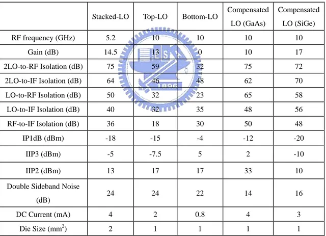
Table 2-1: The 2LO-to-RF Isolations of Active Gilbert Sub-Harmonic Mixers………....…..22
Table 2-2: The Simulated Noise Contribution of Each Device for The Active Sub-Harmonic Mixers………..…...…...27
Table 2-3: The Measured Performances……….….30
Table 2-4:The Comparisions of the IIP2 of Sub-Harmonic Gilbert Mixers……….……...36
Table 2-5: The Measured Performances of the Demonstrated Sub-Harmonic Mixers………44
Table 3-1: The Measured Performances of the Demonstrated Up-Conversion Mixers………...72
Table 4-1: The quadrature signals of the RF, the image, the error RF and the error image signals generated by the quadrature generator……….…..75
Table 4-2: The downconverted IF signals of the desired and image signals with LO signals (neglecting the high frequency components)……….………...76
Table 4-3: The downconverted IF signals considering the imperfect quadrature signals (neglecting the high frequency components)………...……..….79
Table 4-4: The Comparison of Silicon Image Rejection Mixers………..…...87
Table 5-1: Summary of the Weaver-Hartley Down-Donverter Using 0.18 um CMOS Technology….137 Table 5-2: Comparison of the Dual-Band Down-Donverter Architectures………...137
Table 5-3: Summary of the Weaver-Hartley Down-Donverter Using 0.35 um SiGe HBT Technology………...146
Figure Captions
Chapter 1Fig. 1-1. The HBT layer structure including emitter ledge………3 Fig. 1-2. The prediction of the CMOS scaling roadmap made by the ITRS……….4 Fig. 1-3. The cost for (a) digital scaling and (b) the RF scaling……….…...5 Fig. 1-4. The R&D cost of the deep sub-micron CMOS technology. (Estimated by TSMC)…………...5
Chapter 2
Fig. 2-1. The schematic of the 5.2 GHz three-level stacked-LO sub-harmonic GaInP/GaAs HBT Gilbert downconversion mixer………...12 Fig. 2-2. (a) The simplified schematic of the three-level stacked-LO mixer, and (b) the timing diagram of the stacked-LO Gilbert cells………..14 Fig. 2-3. The schematics of the (a) top-LO-configured; and (b) bottom-LO-configured leveled-LO
sub-harmonic mixers………..15 Fig. 2-4. The simulated ratio of the modified Bessel function as a function of the LO input voltage
VBE……….17
Fig. 2-5. The die photos of (a) the 5.2 GHz stacked-LO sub-harmonic mixer, (b) the 10 GHz top-LO-configured sub-harmonic mixer, and (c) the 10 GHz bottom-LO-configured sub-harmonic mixer………...20 Fig. 2-6. The measured and simulated LO-to-IF, 2LO-to-IF, LO-to-RF, and 2LO-to-RF isolations as a
function of the LO frequency for the stacked-LO sub-harmonic mixers……...………20 Fig. 2-7. The measured LO-to-IF, 2LO-to-IF, LO-to-RF, and 2LO-to-RF isolations as a function of LO frequency for the top-LO-configured and bottom-LO-configured sub-harmonic mixers….21 Fig. 2-8. The measured and simulated RF-to-IF isolations as a function of RF frequency of the
top-LO-configured and bottom-LO-configured sub-harmonic mixers………..22 Fig. 2-9. The measured and simulated conversion gain as a function of the LO power of the stacked-LO,
and leveled-LO mixers………...23 Fig. 2-10. The measured and simulated IP1dB and IIP3 of the stacked-LO sub-harmonic GaInP/GaAs
HBT Gilbert downconversion mixer………..24 Fig. 2-11. The P1dB, IIP3 and IIP2 of the top-LO-configured and bottom-LO-configured sub-harmonic mixers……….25 Fig. 2-12. Measured low-frequency noise spectrum of the GaInP/GaAs HBT (AE=2x6um2, IC=0.85mA,
Fig. 2-14. The measured and simulated conversion gain as a function of the IF frequency of the top-LO-configured and bottom-LO-configured sub-harmonic mixers………..28 Fig. 2-15. The measured return loss of the stacked-LO, top-LO-configured, and bottom-LO-configured sub-harmonic mixers………..29 Fig. 2-16. The conventional stack-LO doubler with the time delay effect………..31 Fig. 2-17. (a) A simple multiplier; and (b) a block diagram of the phase-delay cancelled multipliers
pair……….32 Fig. 2-18. Fully symmetrical 2LO cell with the time delay compensation ability (neglecting the biasing
circuits)………...33 Fig. 2-19. The circuit schematic of the GaInP/GaAs HBT 10 GHz double-balanced sub-harmonic mixer with the LO time-delay compensation………...34 Fig. 2-20. The circuit schematic of the double balanced SiGe BiCMOS 10 GHz sub-harmonic
down-conversion micromixer for compensating the LO time-delay neglecting some biasing circuits………34 Fig. 2-21. The photomicrograph of the GaInP/GaAs HBT 10 GHz sub-harmonic mixer with the LO
time-delay compensation………...35 Fig. 2-22. The measured power performances of the 10 GHz sub-harmonic mixer with the LO
time-delay compensation………...36 Fig. 2-23. Measured low-frequency noise spectrum of the HBT (AE = 2X4 um 2, IC=2.8 mA, and IB =
3 uA)……….….37 Fig. 2-24. The measured and simulated double sideband noise figure and conversion gain of the 10
GHz sub-harmonic micromixer as a function of IF frequency………..38 Fig. 2-25. Measured low-frequency noise spectrum of the SiGe bipolar transistor (AE = 0.3 X 9.9 um 2, and IB = 1.6 uA)………39 Fig. 2-26. The die photograph of the SiGe BiCMOS 10 GHz sub-harmonic down-conversion mixer for compensating the LO time-delay………...40 Fig. 2-27. The measured and simulated results of the conversion gain as a function of LO input power
of the down-conversion sub-harmonic mixer using the SiGe BiCMOS technology…….…41 Fig. 2-28. The measured power performance of the 10 GHz sub-harmonic mixer using the SiGe
BiCMOS technology……….…….41 Fig. 2-29. The measured and simulated LO-to-RF and 2LO-to-RF isolations of the sub-harmonic mixer using the SiGe BiCMOS technology……….42 Fig. 2-30. The measured and simulated LO-to-IF and 2LO-to-IF isolations of the sub-harmonic mixer
using the SiGe BiCMOS technology……….43 Fig. 2-31. The measured and simulated IF bandwidth and the double sideband noise figure of the
Fig. 3-1. Schematic of the 5.2 GHz SiGe upconverter using the output LC current mirror and the LO lumped balun………..47 Fig. 3-2. Photograph of the 5.2 GHz SiGe upconverter using the output LC current mirror and the LO lumped balun………..47 Fig. 3-3. (a) The typical rat-race hybrid; (b) Output balance signals; (c) Signal cancelation at port 4; (d) Impedance of the input port………...49 Fig. 3-4. The lumped-element rat-race balun………...50 Fig. 3-5. The LC current combiner operational principle. The inductor loss is included in the
analysis………...52 Fig. 3-6. The operational principle of the LC current mirror when the inductor has ohmic loss………54 Fig. 3-7. The similar concept between the active current mirror and the LC current mirror. The
common mode feedback circuitry for the active differential load is neglected for simplicity………56 Fig. 3-8. The output power transfer of the LC current mirror and the output buffer………...57 Fig. 3-9. The block diagram of the common-collector output buffer……….….59 Fig. 3-10. The output impedance of the common-collector output buffer as a function of
frequency………61 Fig. 3-11. Meaured and simulated Conversion gain vs. LO power of the 5.2 GHz SiGe upconverter using the output LC current mirror and the LO lumped balun………..62 Fig. 3-12. IF port input return loss and RF port output return loss of the 5.2 GHz SiGe upconverter
using the output LC current mirror and the LO lumped balun………..63 Fig. 3-13. Power performance of the 5.2 GHz SiGe upconverter using the output LC current mirror and the LO lumped balun………..63 Fig. 3-14. Measured and simulated LO-to-RF and LO-to-IF isolations of the 5.2 GHz SiGe HBT
upconverter……….64 Fig. 3-15. Measured RF output bandwidth of the 5.2 GHz SiGe HBT upconverter using the output LC current mirror and the LO lumped balun………...……65 Fig. 3-16. The IF input bandwidth of the 5.2 GHz SiGe HBT upconverter using the output LC current mirror and the LO lumped balun………65 Fig. 3-17. Schematic diagram of the GaInP/GaAs HBT Gilbert upconverter with the lumped rat-race hybrid and the LC current combiner………..66 Fig. 3-18. Photograph of the GaInP/GaAs HBT Gilbert upconverter with the lumped rat-race hybrid and the LC current combiner……….67 Fig. 3-19. Power Performance of the GaInP/GaAs HBT Gilbert upconverter with the lumped rat-race
hybrid and the LC current combiner………..68 Fig. 3-20. The schematic of the upconversion micromixer using the active-inductor LC current
Fig. 3-21. The photograph of the upconversion micromixer using the active-inductor LC current mirror……….70 Fig. 3-22. Power performances of the upconversion micromixer using the active-inductor LC current
mirror……….71 Fig. 3-23. The conversion gain as a function of the RF frequency of the upconversion micromixer using
the active-inductor LC current mirror………..………..71
Chapter 4
Fig. 4-1. Block diagram of a double quadrature downconversion mixer with polyphase filters…….…75 Fig. 4-2. The illustration of the nodes connection at the output ports to cancel the RFERxLOID
signals………..………...78 Fig. 4-3. The schematic of the Gilbert mixer used in this work………..79 Fig. 4-4. The schematic of the output buffer used in this work………...80 Fig. 4-5. Photograph of a SiGe HBT double quadrature downconverter with polyphase filters……….81 Fig. 4-6. Measured and simulated conversion gain as a function of the LO power of the SiGe HBT double quadrature downconverter with polyphase filters………..82 Fig. 4-7. Measured and simulated LO-to-IF isolation of the SiGe HBT double quadrature
downconverter with polyphase filters……….………...………83 Fig. 4-8. Measured and simulated RF-to-IF isolation of the SiGe HBT double quadrature
downconverter with polyphase filters………83 Fig. 4-9. One tone power measurements of the SiGe HBT double quadrature downconverter with
polyphase filters……….84 Fig. 4-10. One tone and two tone power measurements of the SiGe HBT double quadrature
downconverter with polyphase filters………84 Fig. 4-11. Conversion gain as a function of IF frequency for the SiGe HBT double quadrature
downconverter with polyphase filters………...….85 Fig. 4-12. Measured and simulated Image rejection ratios of the SiGe HBT double quadrature
downconverter with polyphase filters……….……...85 Fig. 4-13. Measured and simulated RF, IF, and LO return losses of the SiGe HBT double quadrature downconverter with polyphase filters………86 Fig. 4-14. (a) The block diagram of the Weaver down-converter; and (b) the representation of the
Weaver architecture using complex signal mixing approach……….89 Fig. 4-15. The spectrum analysis of the Weaver down-converter using the complex mixing analysis: (a) the original RF and image signals before down-conversion, (b) the signals after down-converted by the first stage complex mixer, and (c) the final signals after down-converted by the first and second stage complex mixers……….91
mismatches are considered. (a) The desired IF signal, (b) the unwanted image signal caused by signal mismatches, and (c) the final mixed signals……….…..93 Fig. 4-17. The ADS simulation results of the image rejection ratio influenced by different LO phase mismatches……….96 Fig. 4-18. (a) The simulated image rejection ratio as a function of phase error φε2of the LO2 signal and the phase error φε1 of the LO1 signal, and (b) a simplified simulated image rejection ratio as a function of LO1 and LO2 phase errors……….96 Fig. 4-19. The total schematic of the 5.2/5.7 GHz GaInP/GaAs HBT 48 dB image rejection Weaver down-converter……….….99 Fig. 4-20. The schematic of the micromixer used as the first stage mixer……….….99 Fig. 4-21. The schematic of the Gilbert mixer used as the second stage mixer……….…100 Fig. 4-22. The schematic of (a) the adder, (b) the subtraction cell, and (c) the output buffer……....101 Fig. 4-23. (a) The schematic of the highly symmetrical frequency multiplier, and (b) the block diagram of the multiplier………103 Fig. 4-24. The schematic of the frequency quadrupler used to correlate the LO1 and LO2
signals………...104 Fig. 4-25. The die photo of the 5.2/5.7 GHz GaInP/GaAs HBT 48 dB image rejection Weaver
down-converter using LO frequency quadrupler……….105 Fig. 4-26. The measurement results of the conversion gain as a function of LO input power of the
Weaver down-converter when input RF frequency is 5.7 GHz and input RF frequency is 5.2 GHz respectively………..106 Fig. 4-27. The measured image rejection of the proposed Weaver down-converter (a) when the RF
frequency is 5.2 GHz and the image signal is 2.8 GHz; (b) when the RF frequency is 5.7 GHz and the image signal is 3.1 GHz………..106 Fig. 4-28. The measured power performance as a function of RF input power of the Weaver
down-converter when RF frequency is 5.7 GHz………..108 Fig. 4-29. The measured power performance as a function of RF input power of the Weaver
down-converter when RF frequency is 5.2 GHz………..109 Fig. 4-30. The measured and simulated input and output return losses of the Weaver
down-converter………109 Fig. 4-31. The measured RF-to-IF isolation for both I-channel and Q-channel of the Weaver
down-converter………....110 Fig. 4-32. The measured LO-to-IF and LO-to-RF isolations for both I-channel and Q-channel of the
Fig. 5-1. (a) The block diagram of the Weaver-Hartley architecture, and (b) the complex representation of the Weaver-Hartley architecture………..115 Fig. 5-2. (a) The RF, IM1, and IM2 signals before down-converted neglecting the signals located in the
negative frequencies for simplicity; (b) the RF, IM1, and IM2 signals after down-converted by the first stage complex mixer; (c) the signals after down-converted by the second stage complex mixer; and (d) the signals filtered by the IF polyphase filters. All the high frequency harmonics are neglected………..118 Fig. 5-3. The block diagram of a double-quadrature system with non-ideal input signals………120 Fig. 5-4. All the high frequency harmonics are neglected. (a) The frequency shifting by the negative LO1 and negative LO2 complex signals when the RF frequency is around 5.7-GHz band; and (b) the frequency shifting by the positive LO1 and negative LO2 complex signals when the RF frequency is around 2.4-GHz band………..122 Fig. 5-5. A block diagram of the demonstrated Weaver-Hartley double-quadratrue down-converter
using 0.18 um CMOS technology………123 Fig. 5-6. The schematic of the Gilbert mixers used for the (a) first-stage and (b) second-stage
mixers………...124 Fig. 5-7. (a)The block diagram of the 50% duty-cycle divided-by-five circuit and (b) the timing
diagram……….…125 Fig. 5-8. (a) The schematic of the source couple logic D flip-flops, and (b) the true table…………...126 Fig. 5-9. The truly balanced multiplier………..127 Fig. 5-10. The LO1 signal polarization switching circuit used to perform the band selection………...127 Fig. 5-11. The die photo of the Weaver-Hartley down-converter using 0.18 um CMOS
technology………128 Fig. 5-12. The conversion gain as a function of LO power of the demonstrated Weaver-Hartley
down-converter………....129 Fig. 5-13. The power performances of the demonstrated Weaver-Hartley down-converter…………..130 Fig. 5-14. The conversion gain as a function of RF and image frequencies of the demonstrated
Weaver-Hartley dual-band low-IF down-converter. IF frequencies are employed to represent the RF and image frequencies by properly folding the RF and image frequencies into the IF axis (a) RF near 5.7 GHz. (b) RF near 2.4 GHz………..131 Fig. 5-15. The Image rejection ratio of the first image signal and the secondary image signal when (a)
the desired signal is 5.7-GHz and (b) 2.4-GHz………133 Fig. 5-16. The measured input return loss of the Weaver-Hartley down-converter………...134 Fig. 5-17. The measured IQ waveform of the demonstrated Weaver-Hartley dual-band low-IF
down-converter………....134 Fig. 5-18. The measured and simulated RF-to-IF isolation………...135 Fig. 5-19. The measured and simulated LO-to-RF, and LO-to-IF Isolations………136
down-converter………....136
Fig. 5-21. A block diagram of the demonstrated Weaver-Hartley double-quadratrue down-converter using 0.35 um SiGe BiCMOS technology………...138
Fig. 5-22. (a) The block diagram of the divided-by-2 circuit of the LO generator, (b) the topology of the divided-by-2 circuit of the LO generator, (c) the circuit topology of the frequency doubler, and (d) the single sideband mixer……… ...139
Fig. 5-23. Die photo of the demonstrated Weaver-Hartley double-quadratrue down-converter using 0.35 um SiGe BiCMOS technology……….…140
Fig. 5-24. The conversion gain as a function of RF frequencies of the demonstrated Weaver-Hartley down-converter using 0.35 um SiGe BiCMOS technology. (a) The desired RF frequencies locate from 5.675 GHz to 5.77 GHz. (b) The desired RF frequencies locate from 2.425 GHz to 2.33 GHz………..141
Fig. 5-25. The Image rejection ratio of the first image signal and the secondary image signal when (a) the desired signal is 5.7 GHz and (b) 2.4 GHz………....142
Fig. 5-26. The measured and simulated input return loss of the Weaver-Hartley down-converter…...143
Fig. 5-27. The measured IQ waveform of the demonstrated Weaver-Hartley down-converter using 0.35 um SiGe BiCMOS technology……….…144
Fig. 5-28. The measured and simulated RF-to-IF isolation………...144
Fig. 5-29. The measured and simulated LO-to-RF, and LO-to-IF Isolations………145
Fig. 5-30. The measured single sideband noise of the Weaver-Hartley down-converter………..145
Fig. 5-31. The power performances of the demonstrated Weaver-Hartley down-converter…………..146
Chapter 6 Fig. 6-1. (a) The circuit schematic of the Meyer wideband amplifier (b) and the Kukielka amplifier………...149
Fig. 6-2. The block diagram of the Meyer wideband amplifier……….151
Fig. 6-3. (a) The A circuit and βV circuit of the Meyer Amplifier after first decomposition, and (b) the A circuit and βI circuit after second decomposition………152
Fig. 6-4. The final topology of modified Meyer wideband amplifier………157
Fig. 6-5. The small signal model for solving (a) the first pole and (b) the second pole………....158
Fig. 6-6. The small signal model of the Darlington stage used to solve the frequency response……..159
Fig. 6-7. The demonstrated 0.13 µm CMOS Meyer wideband amplifier with its component values………...164
Fig. 6-8. The die photograph of the 0.13 µm CMOS shunt-series series-shunt double feedback amplifier………...165
Fig. 6-9. The measured S21, and the S21 predicted by our theory of the 0.13 µm CMOS Meyer wideband amplifier………...165
wideband amplifier………..166 Fig. 6-11. The measured S22, and the S22 predicted by our theory of the 0.13 µm CMOS Meyer
wideband amplifier………..167 Fig. 6-12. The measured noise figure of the 0.13 µm CMOS Meyer wideband amplifier…………....167 Fig. 6-13. The measured power performance of the 0.13 um CMOS Meyer wideband amplifier……168
Chapter 7
Fig. 7-1. The block diagram of (a) the double-quadrature Weaver with double-quadrature Hartley architecture, and (b) the single-quadrature Weaver with double-quadrature Hartley architecture………..171 Fig. 7-2. The illustration of the frequency shifting (down-converting) of the single quadrature
Weaver-Hartley system………172 Fig. 7-3. The block diagram of (a) the double-quadrature Hartley with double-quadrature Hartley
architecture, and (b) the single-quadrature Hartley with double-quadrature Hartley architecture………..173 Fig. 7-4. The illustration of the frequency shifting (down-converting) of the single quadrature
Hartley-Hartley system………174 Fig. 7-5. The block diagram of (a) the double-quadrature Weaver with direct-conversion architecture, and (b) the single-quadrature Weaver with direct-conversion architecture……….175 Fig. 7-6. The illustration of the frequency shifting (down-converting) of the single quadrature Weaver with direct-conversion system……….176 Fig. 7-7. The block diagram of (a) the double-quadrature Hartley with double-quadrature
direct-conversion architecture, and (b) the single-quadrature Hartley with double-quadrature direct-conversion architecture……….177 Fig. 7-8. The illustration of the frequency shifting (down-converting) of the single quadrature Hartley
with direct-conversion system……….178
Appendix A
Fig. A-1. The block diagram of (a) the Weaver architecture, and (b) the Hartley architecture.……….187
Chapter 1
Introduction
The RFICs (Radio Frequency Integrated Circuit) become the key building block of the telecommunication circuit in the past decade. Conventionally, the RFIC pursued the high performance at the high frequency region, and the MESFET, GaInP/GaAs HBT, BiCMOS, and PHEMT technologies had played the dominant roles. In this dissertation, the research results start from conventional circuit topology using the advanced technology, and end with novel circuit schematic using the main stream silicon technology.
Many high performance RFICs with conventional circuit topologies are demonstrate using the 2 um GaInP/GaAs HBT technology. There are some unique advantages within the GaInP/GaAs HBT technology: the semi-insulating substrate, high mobility, and the low phase noise. The intrinsic GaAs material has wide band gap when compared with silicon, and the carrier concentration of the GaAs substrate
is about 107/cm2 [1], which is 1000 times lower than the silicon substrate. Therefore,
the GaAs substrate is a high-resistivity substrate, and conventionally called “semi-insulating”. The advantage of the semi-insulating substrate is that the notorious substrate coupling can be totally eliminated, and the RF performance can be improved. For instance, the LO substrate leakage of the Gilbert mixer [2] can be eliminated. In Chapter 2, the state-of-the-art 2LO-to-RF isolation of the direct-conversion sub-harmonic Gilbert mixer [3] is achieved because the 2LO-to-RF substrate coupling is eliminated.
In addition to the elimination of the unwanted coupling substrate, the semi-insulating substrate also helps to provide accurate on-chip passive element. The quality factors as well as the accuracies of the passive elements on the silicon substrate are very difficult to maintain. The substrate parasitics inevitably degrades the quality factor of the on-chip inductors and capacitors [4]. The semi-insulating substrate assures high Q on-chip capacitor because the parasitic substrate capacitances and resistances are eliminated in the semi-insulating substrate. In Chapter 3, accurate
on-chip rat-race hybrids [5] consisting of the inductors and capacitors are demonstrated. The high-performance rat-race hybrids are employed in the up-conversion Gilbert mixers, and thus the up-converters exhibit excellent RF performances.
A major research topic in this dissertation is the image rejection architectures, and all the image rejection systems require quadrature signals. The RC-CR polyphase filters [6] are often used to generate quadrature signals. The quadrature accuracy of the polyphase filters relies on precision resistors and capacitors. The poly silicon resistor has been widely used in the advanced silicon technology, but the process variation is typically larger than 20%. For instance, the typical sheet resistance of the
P+-poly resistor without silicide is 311 Ω per square with 20% error in the 0.18 um
CMOS technology. Although the sheet resistance of the P+-poly resistor with silicide
is 7.8 Ω per squareand the low resistance is adequate to implement the quadrature
generator, the typical process variation of this on-chip resistor is about 30%. On the other hand, the thin film resistors provided by the GaInP/GaAs HBT technology is accurately fabricated because the thickness of the film can be precisely in-situ monitored during the fabrication. In Chapter 4, a high performance Weaver image rejection down-converter [7] is demonstrated using the GaInP/GaAs HBT technology.
The final advantage of the GaInP/GaAs HBT technology is its low 1/f noise corner. The CMOS transistor suffers from the 1/f noise because the inversion layer is
located adjacent to the Si-SiO2 interface. Many dangling bonds (traps) existing in this
interface make the device 1/f noise worse. On the other hand, the ledge of the HBT structure [8] as shown in Fig. 1-1, and the low DX centers of the GaInP/GaAs material make the 1/f noise of the HBT device minimized. The 1/f noise is very important for the RF circuits especially the oscillator and the direct-conversion mixer. The 1/f noise of the mixer can directly influence the output of the mixer, and the CMOS direct-conversion Gilbert mixer is suffered from the worse 1/f noise performance of the CMOS device [9]. The experimental results show that the GaInP/GaAs HBT has 1/f noise corner as low as 400-Hz (depend on the bias condition and the emitter area), and several excellent direct-conversion sub-harmonic Gilbert mixers with less influence of 1/f noise are demonstrated in Chapter 2.
SI substrate Subcollector Collector Base Ledge Ledge GaAs n+ n G a A s+ n GaAs p GaAs+ n InGaAs+ n InGaP 8 0 0 A D 19 3 4 10 (× cm−) Emitter 6000 A D 510 A D
670A
D 16 3 2 10 (× cm−) 17 3 3x10 (cm−)Fig. 1-1.The HBT layer structure including emitter ledge.
In general, the compound technologies such as GaAs HBT and PHEMT are considered as “Advanced but Expensive”, because the compound technologies above are very difficult to be integrated with the baseband chip. As the silicon-based technology improves rapidly, the RF-baseband SOC solution becomes possible. Commercially available 5 GHz WLAN transceivers except power amplifiers (PAs) have been using advanced CMOS and SiGe BiCMOS technology recently. It is commonly believed that RFICs made by silicon technology, especially the CMOS technology, have the lowest cost and can be easily integrated with digital CMOS ICs to form a wireless system on chip (SOC). CMOS transceivers integrated with the digital CMOS ICs have been successfully demonstrated, and so as to make the silicon technology more attractive. However, it is still difficult to integrate the high power PA with the RF transceiver. There exist stand-alone high power CMOS PAs [10] and SiGe PAs for 2.4 GHz WLAN applications [11]. The strong coupling in the Silicon substrate makes it difficult to merge the power amplifier into the RF transceiver. Thus, the PAs at 5 GHz are stand-alone and dominated by the GaAs technology.
As the CMOS device scaling by deep submicron technology continues, the cost of fabrication becomes very high and the device operating voltage decreases. Thus, the integration of high power amplifiers with the SOC becomes more difficult.
Moreover, the size of RFICs does not follow the scaling rule as the digital IC does. It is worthwhile to mention that the cost of research and development for the deep submicron CMOS IC design has increased dramatically due to the high cost photo masks. The high R&D cost has set a big barrier for many companies to enter the wireless IC markets.
In the past, the CMOS technology is very cost effective when compared with the 2 um GaInP/GaAs HBT technology. As the channel length shrinking, the barrier (the R&D cost) of the deep submicron CMOS is already higher than that of the 2 um
GaInP/GaAs. A rough estimation of the cost per mm2 (USD/mm2) of the 0.13 um
CMOS technology for the RF application (including ultra think metal for on-chip
inductors) is 5,300 USD/mm2, and that for 2 um GaInP/GaAs HBT technology is 60
~121 USD/mm2 only. The cost of 0.13 um CMOS technology is 44 times of the cost
of GaAs HBT technology! As shown in Fig. 1-2, the prediction of the CMOS scaling roadmap [12] made by the ITRS (International Technology Roadmap for Semiconductors) predicts that the gate length shrinking becomes very challenging.
Fig. 1-2. The prediction of the CMOS scaling roadmap made by the ITRS. [2]
Although it is believed that the cost can be lower down when the final product is entering mass production (may not be true for the nano tubes), the barrier makes it very hard to finish a final product. The concept of the barrier for the CMOS R&D cost is illustrated in Fig. 1-3(a) and (b). The Y-axis is the cost and the X-axis might be the
product phase. Fig. 1-3(a) shows the cost reduction of the digital circuit as CMOS scaling, and the Fig. 1-3(a) is similar to a conventional diagram of the activation energy. On the other hand, the diagram for the RFIC is shown in Fig. 1-3(b) when the size of the CMOS is scaled down. Only when the RF solution provider expanses enormous investment, the final product can be realized. Figure. 1-4 manifests the same idea and depicts the R&D cost estimated by TSMC [13]. The average R&D cost of the 0.13 um CMOS is about 10 million USD, and the cost of 65 nm CMOS is as high as 45 million USD!
R&D Production Phase 65 nm CMOS 0.18 um CMOS 0.5 um CMOS Digital IC Cost 65 nm CMOS 90 nm CMOS 0.5 um CMOS 2 um GaInP/GaAs HBT R&D Phase Production RFIC Cost (a) (b) Fig. 1-3. The cost for (a) digital scaling and (b) the RF scaling.
GaInP/GaAs HBT PAs are made by lower-cost 2 um photolithography. The cost for photo masks with 2 um accuracy is much lower than that for photo masks with 0.13 um accuracy. Thus, the IC design R&D cost for HBT technology is significantly lower than that for deep submicron CMOS technology. Conventionally, GaInP/GaAs HBT technology needs only roughly 10 mask steps while CMOS technology has more than 20 mask steps. There already exist 6-inch GaAs fabs when compared with the 12-inch Si fabs. Thus, there is a chance that the production cost for GaAs HBT RF transceivers can be lower down when compared with CMOS RF transceivers. If the external GaInP/GaAs HBT PA is still unavoidable, it is straightforward to think of the possibility of integrating the whole transceiver including PAs in GaInP/GaAs HBT technology because the semi-insulating GaAs substrate eliminate the cross coupling between the PA with the RF transceiver. In this work, several high-performance RFIC building blocks are demonstrated in 2 um GaInP/GaAs HBT technology. The research result shows that it is possible to accomplish a fully integrated RFIC including the power amplifier. It is might be another choice for the RF SOC.
Recently, there is a new trend to design the RF transceiver in the digital domain: the software-defined radio [14] and the DRP (Digital RF Processor) architecture [15]. These efforts are reducing the complexity of the RF transceiver and move the functions into the digital domain. Although these new concepts are interesting, there are still some serious drawbacks. In order to demodulate or convert the analog signal to digital domain, a high-speed and high-resolution A/D converter with high power consumption is required [14]. In addition, the down-conversion process is more difficult and can not be real time when the RF signals are distorted too much [14].
In this dissertation, in addition to the RFICs in GaInP/GaAs HBT technology, other high performance silicon based RFICs with novel circuit topologies are also demonstrated for completeness. The research results demonstrated in this dissertation include the image rejection low-IF architecture, direct-conversion sub-harmonic Gilbert mixers, fully integrated up-convertors, and shunt-series series-shunt double feedback amplifiers. The demonstrated RF circuits are implemented using the GaInP/GaAs HBT, SiGe BICMOS, and CMOS technologies.
mixers are described in Chapter 2. Next the Chapter 3 introduces the high performance up-conversion mixers. Chapter 4 discusses the conventional image rejection down-converters including Hartley and Weaver systems. The novel Weaver-Hartley dual-band down-converter is demonstrated in Chapter 5. The shunt-series series-shunt double feedback amplifier is described in Chapter 6. Finally, Chapter 7 concludes this dissertation and discusses the future work.
The super-heterodyne system is a reliable system through many years. The low-IF system [16][17] and the direct-conversion system [18] are presented in order to increase the integration level. The image rejection off-chip filter can be removed in the low-IF system because the IF polyphase filter is used to eliminate the image IF signal in the Hartley system [6][16][17]. In addition to the Hartley system, the Weaver system is the other practical receiver architecture to reject the image signal without the off-chip image rejection filters. The Weaver system cleverly utilizes the frequency shifting technique to block the unwanted image signals. The down-converted image signal can be totally rejected by the lowpass filter or the frequency response of the output amplifier.
The direct-conversion architecture is a highly integrated system. This compact system suffers from the notorious self-mixing problem. In order to eliminate the image signal, the IF frequency of the direct-conversion system is set to be zero. However, the LO frequency is the same with the RF frequency and thus the LO signal can be down-converted to the IF band if the LO signal leaks to the RF port. The above scenario is the cause of the self-mixing.
Many sub-harmonic direct-conversion Gilbert mixers are demonstrated in Chapter 2. The conventional stacked-LO, top-leveled-LO, and bottom-leveled-LO sub-harmonic mixers are demonstrated using the 2 um GaInP/GaAs HBT technology. The design trade-offs of the sub-harmonic mixers are discussed in detail. In addition, a novel LO-compensated highly symmetrical Gilbert sub-harmonic mixer topology is
proposed. The new sub-harmonic mixer demonstrates excellent IIP2 and 2LO-to-RF
isolation when the RF frequency is 10 GHz.
Chapter 3 introduces a systematic analysis of the up-conversion Gilbert mixer using the lumped-element rat-race hybrid and the passive L-C current mirror. The
design consideration of the L-C current mirror including the parasitic resistance of the on-chip inductors is established. In addition to the passive inductor, a version of the up-conversion mixer with the active inductor is demonstrated. The active inductor successfully saves the valuable chip area at the expense of the dynamic range.
In the dissertation, a 0.35 um SiGe HBT Hartley image rejection down-converter is demonstrated in Chapter 4. This 5.2 GHz down-converter can provide image rejection ratio up to 47 dB. A 2 um GaInP/GaAs HBT 5.2/5.7 GHz Weaver down-converter is also presented in Chapter 4. The image rejection ratio of the Weaver down-converter is 48 dB.
Chapter 5 presents a novel dual band Weaver-Hartley architecture. A 0.35 um SiGe and a 0.18 um CMOS 5.7/2.4 dual band Weaver-Hartley systems are demonstrated. Both circuits exhibit 40 dB image rejection ratio for the band selection using the Weaver system and 46 dB image rejection ratio for the adjacent channel image signal using the polyphase filter.
Finally, a 0.13 um CMOS wideband amplifier is demonstrated in Chapter 6. The wideband amplifier is the well-known Meyer topology, and this amplifier contains double feedback loops. The design formulas of the shunt-series series-shunt double feedback amplifier are discovered. The experimental results of the S parameters are highly agreed with our theory and the insight of the Meyer amplifier is obtained in this chapter.
Chapter 2
High Performance Direct-Conversion
Sub-Harmonic Gilbert Mixers
Among all the receiver architectures, the most popular system is the direct-conversion system [18]. The direct-conversion mixer is the most challenging topics when compared with the mixers used in the low-IF system [16][17]. The direct conversion system is the simplest system while the mixer is hardest to be designed. In this chapter, we start from conventional direct-conversion sub-harmonic Gilbert mixers using the advanced technology and end with a novel sub-harmonic Gilbert mixer topology.
More and more RF transceiver architectures are proposed because the wireless communication applications grow rapidly. The heterodyne system has been used for many years; however, the off-chip image rejection SAW filter limits the circuit integration of the heterodyne system. The active or passive polyphase filters are used in the low-IF system to filter out the image signal, but the polyphase filters occupy too many valuable IC estates [6], [17]. The direct-conversion architecture is proposed to increase the integration level. The direct-conversion system eliminates many bulky and expensive off-chip components, such as image-rejection and channel-select filters [18]. The RF frequency is arranged to be equal to the LO frequency in the direct-conversion system and thus the image signal is the RF signal itself. As a result, the image-rejection filter is no longer necessary. The direct-conversion structure reduces the manufacture cost and improves the circuit integration.
The direct-conversion transceiver is highly integrated at the cost of many novel problems such as the DC offset, the LO leakage, the I/Q signal mismatch, the even-order distortion and the flicker noise. Most important of all, the LO frequency of the direct-conversion mixer is too close to the RF frequency so that the self-mixing problem caused by the LO leakage can degrade the transceiver performance. In order to prevent the self-mixing problem, the sub-harmonic mixer topologies are proposed [3], [19]-[22].
Conventionally, the passive harmonic mixers have been used for many years. The passive diode mixers using the nonlinear property of the diodes and these mixers
have super gain compression point (IP1dB) at the cost of larger conversion loss and
larger LO pumping power. On the other hand, sub-harmonic Gilbert mixers usually provide conversion gain at the cost of slower operation speed.
Three distinct sub-harmonic Gilbert mixers topologies based on the double-balanced structure have been proposed. The first topology is the three-level stacked-LO structure [3], [19], [20]. The working principle of the stacked Gilbert cell is to mix down the RF signal with the quadrature LO signals. On the contrary, the top-LO-configuration [21], and the bottom-LO-configuration [22] mixers are the leveled-LO sub-harmonic structures and their operations are based on the transistor’s nonlinearity. In this work, all three different types of the conventional sub-harmonic Gilbert mixers are demonstrated using GaInP/GaAs HBT technology for the first time to the best of our knowledge. The pros and cons of the conventional sub-harmonic Gilbert mixers are discussed.
Ideally, the double balanced sub-harmonic mixer can totally eliminate the 2LO leakage; however, the 2LO leakage occurs when non-ideal effects such as circuit mismatches and the imperfections of the LO signal take place. In addition, the self-mixing problem caused by the 2LO leakage is more pronounced through the substrate coupling. The isolation properties can be improved using the deep N-well in the advance CMOS technologies [23] and the deep trench isolation in the SiGe bipolar technology [24]. Compared with the silicon substrate, the GaInP/GaAs HBT technology possesses a perfect semi-insulating substrate, and thus the high frequency 2LO leakage signal can not leak to the RF port through the GaAs substrate. Because the substrate coupling is eliminated in this work, the 2LO-to-RF isolation performances among the Gilbert sub-harmonic mixer topologies can be fairly investigated. According to our experimental results, the stacked-LO sub-harmonic mixer is the best topology to achieve the highest 2LO-to-RF isolation.
It is easy to generate accurate quadrature signals in the GaInP/GaAs HBT technology. Almost all the published sub-harmonic mixers were fabricated on the
lossy silicon substrates [21]-[24]. The effectiveness of the quadrature signals is limited by the fabrication variation and the silicon substrate parasitic effect. However, the LO quadrature generator, which is often a polyphase filter [6], can be implemented precisely using GaInP/GaAs HBT technology because of the accurate
thin film resistors with 50 Ω sheet resistance, the 0.36 fF/um2
MIM Si3N4 capacitors, and the semi-insulating GaAs substrate. It is noticed that a capacitor in the standard silicon process has a smaller area and thus suffers more from fabrication variation
because of the 1 fF/um2 MIM capacitor employed in the silicon process.
Because the passivated ledge is employed over the extrinsic base surface [8], [25] and the DX center trap in the GaInP material is absent, the GaInP/GaAs HBT technology has low flicker noise. According to the previous literatures [9], [26], [27], the 1/f noise dominates the low frequency noise figure in the direct-conversion mixer. The HBT device in this work has very low 1/f noise and the measured slope of the mixer noise figure as a function of the IF frequency validates this characteristic.
2.1 Conventional Sub-Harmonic Gilbert Mixers
In this section, the design trade-offs among the conventioanl sub-harmonic Gilbert mixers are discussed. Each sub-harmonic mixer topology has its own advantage. The stacked-LO structure [28] requires a smaller LO pumping power, but inevitably needs a larger DC supply voltage. The cascode stacked-LO structure makes the 2LO leakage very difficult to leak to the RF port, and thus the best 2LO-to-RF isolation is achieved in this structure.
On the other hand, the leveled-LO mixers can be potentially operated at higher frequency but needs a larger LO pumping power. When compared with the stacked-LO mixer, the leveled-LO mixers can operate at higher frequencies because this LO stage operates using the transistor’s nonlinearity. The leveled-LO mixers (both the bottom-LO-configuration and the top-LO-configuration mixers) are likely to be faster than the stacked-LO mixer. The bottom-LO-configuration is the simplest topology, but it provides a smaller conversion gain and poor 2LO-to-RF isolation. The bottom-LO-configuration provides the minimal port-to-port isolation due to the circuit
topology.
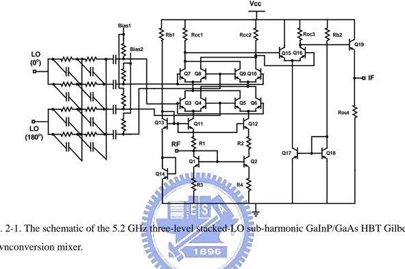
The stacked-LO mixer with two Gilbert cells consumes smaller current because the DC current is reused in the cascode structure. The stacked-LO sub-harmonic Gilbert mixer has two LO ports and one RF port, as shown in Fig. 2-1.
LO (0o) Bias1 Bias2 IF Q3 Q4 Q5 Q6 Q7 Q8 Q9 Q10 Q13 Q14 Q15 Q16 Q17 Rb1 Rcc1 Rcc2 Rcc3 Rb2 Rout RF Q1 Q2 Q11 Q12 Q18 Q19 R1 R2 R3 R4 LO (180o) Vcc
Fig. 2-1. The schematic of the 5.2 GHz three-level stacked-LO sub-harmonic GaInP/GaAs HBT Gilbert downconversion mixer.
The bottom LO Gilbert cell transistors (Q3-Q6) are fed by I+ and I- LO input
signals while the top LO Gilbert cell transistors (Q7-Q10) are fed by Q+ and Q- LO
input signals. If the I-phase and Q-phase LO signals are respectively defined as
cosωLOt and sinωLOt, the equivalent LO signals can be determined as follows:
1
cos sin sin 2
2
LOt LOt LO
ω
⋅ω
=ω
t(2.1)
Hence, the down-converted IF output frequency of the stacked-LO Gilbert mixer is the difference of the RF and the 2LO frequencies. This topology with two stacked HBT-type Gilbert cells only needs very small LO pumping power when compared with the CMOS technologies. Because the transconductance of the HBT is an exponential function of the base-emitter voltage, the current in the LO Gilbert cell can
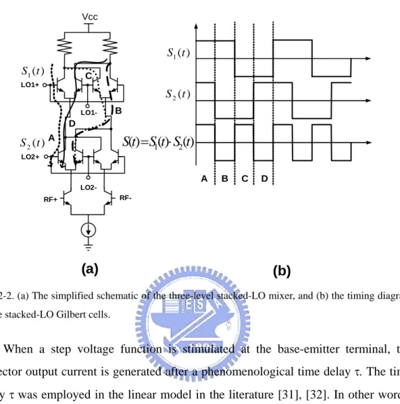
The stacked-LO cell actually provides a composite switching function, and the simplified stacked-LO sub-harmonic mixer is shown in Fig. 2-2(a). The switching
function of the top and bottom Gilbert cells in Fig. 2-2(b) are expressed as S1(t) and
S2(t), respectively. If the signal S1(t) is behind S2(t) by a quarter period, the composite
switching function represented as S(t) is the exclusive OR function of S1(t) and S2(t).
As shown in Fig. 2-2(b), the stacked-LO cell has a switching function S(t), whose switching frequency is doubled. The corresponding paths in the composite switching half-periods A, B, C, and D are drawn in Fig. 2-2(a) and only half of the switching paths are drawn for simplicity.
The stacked-LO Gilbert mixer requires quadrature LO signals, and thus a two-section passive polyphase filter is employed to generate the accurate LO signals. The LO stages are stacked and biased at the different DC levels; hence, four DC blocking capacitors of 2 pF and biasing resistors of 3 kΩ are used in the top and bottom LO stages, as illustrated in Fig. 2-1.
The common-emitter transistor Q2 the common-base transistor Q11 and the
resistors R1 to R4 form the single-to-differential input stage, when Q1 and Q2
constructed as a current mirror (or the micromixer) [29], [30]. The common-base
transistor Q11 possesses good frequency response, and the micormixer topology
achieves the impedance matching at the RF input port. Thus, the chip area is saved. An output buffer consisting of an asymmetric differential amplifier and a common-collector output stage are incorporated to combine the IF output differential signals and to perform the output impedance matching.
The leveled-LO sub-harmonic mixer is an appropriate topology for the high-frequency and low-voltage mixer design. Figures 2-3(a) and (b) show the top-LO-configured leveled-LO mixer [21] and the bottom-LO-configured leveled-LO mixer [22]. By feeding LO signals with proper phases, the even harmonic leveled-LO structure can be employed to commutate RF currents at the rate of 2LO frequency [21]. Compared with the stacked-LO sub-harmonic mixer, the leveled-LO structure uses the transistor’s nonlinearity. The 2um GaInP/GaAs HBT transistor
mA/um2) and BVCEO of13V. LO2+ LO2- LO1-LO1+ RF+ RF-Vcc A D B C 1( ) S t 2( ) S t 1 2
( )
( )
( )
S t
=
S t S t
⋅
A B C D(a)
(b)
1( ) S t 2( ) S tFig. 2-2. (a) The simplified schematic of the three-level stacked-LO mixer, and (b) the timing diagram of the stacked-LO Gilbert cells.
When a step voltage function is stimulated at the base-emitter terminal, the collector output current is generated after a phenomenological time delay τ. The time delay τ was employed in the linear model in the literature [31], [32]. In other words,
the I-V characteristic transfer function should be expressed in terms of VBE, VCE and
τ. The output collector current follows the terminal base-emitter and collector-emitter voltages in an adiabatic way only if the operating radian frequency is much less than the reciprocal of the time delay τ. In general, active circuits operate much slower than the time delay τ which is normally on the order of one-third of the transistor transit-time delay [31], [32]. Therefore, the transit-time cut-off frequency fT is still a good practical indication to judge whether the quasi-static model is valid for the second harmonic frequency or not.
The stacked-LO mixer basically trades the head room with higher 2LO-to-RF isolation. Because the stacked-LO topology has smaller head room, the reused biasing current of the LO cell and the RF input stage can not be very large. On the other hand, there are fewer transistor levels stacked together in the leveled-LO topology and thus
the biasing current can be larger. In other words, the level-LO topology operates at higher transit time cut-off frequency than the stacked-LO topology does.
Vcc RF+ RF-R1 R2 R3 C1 C2 Qa Qb Q1 Q2 Q3 Q4 Q5 Q6 Q7 Q8 LO (0o) LO (180o) IF Qin1 Qin2 (a) LO (0o) LO (180o) Vcc RF+ RF-Q1 Q2 Q3 Q4 Qa Qb R1 R2 R3 C2 C1 Q5Q6 Q7Q8 IF QC Qd RL1 RL2 (b)
Fig. 2-3. The schematics of the (a) top-LO-configured; and (b) bottom-LO-configured leveled-LO sub-harmonic mixers.
An HBT transistor is a nonlinear device with exponential dependence between the collector current and the base-emitter voltage. The top-LO-configuration is shown in Fig. 2-3(a). The emitter-coupled pairs consisting of transistor pairs Q1-Q2 to Q7-Q8
forms the leveled-LO cell when their collectors are connected together. If 0O and 180O
differential input signals are injected into the leveled-LO Q1-Q2 pair, the fundamental
signals are eliminated by shorting the collectors of the differential pair and only the
even harmonic currents appear at the collector nodes. Simultaneously, 90O and 270O
LO signals are injected into the leveled-LO Q5-Q6 pair to generate the 2LO signal that
pairs Q1-Q2 and Q5-Q6 work together to provide perfect 2LO differential signals [21]. Consequently, this structure can be used for the sub-harmonic mixer, and these emitter-coupled leveled-LO pairs shown in Fig. 2-3(a) are able to double the LO frequency.
As shown in Fig. 2-3(a) and (b), the difference between these two types of leveled-LO mixers is the location of the LO cell. The top-LO-configuration mixer
consists of four leveled-LO pairs (Q1 to Q8) above the RF input stage while the
bottom-LO-configuration mixer contains two leveled-LO cells under the RF input stage. The differential-quadrature LO signals of the double-balanced structure used in this work can be generated by a two-section polyphase filter.
In order to discuss the operation mechanism of the leveled-LO topology, the HBT exponential I-V transfer function can be expressed as the modified Bessel
function [33], [34]. As shown in Fig. 2-3(a), the transistors Q1 and Q2 form a
leveled-LO cell. The input LO signals of transistor Q1 and Q2 are defined as two
out-of-phase signals vcosωt
∧
and vcosωt
∧
− , respectively. The output collector
currents can be described as follows:
cos 1 0 1 2 3 cos 2 0 1 2 3
[ ( ) ( ) cos ( ) cos 2 ( ) cos 3 ] (2.2a)
[ ( ) ( ) cos ( ) cos 2 ( ) cos 3 ]
T T v t V CQ S S v t V CQ S S I I e I I x I x t I x t I x t I I e I I x I x t I x t I x t ω ω ω ω ω ω ω ω ∧ ∧ − = = + + + + = = − + − + … … (2.2b)
Where x is equal to the ratio of T v V
∧
. The In(x) in (2.2a) and (2.2b) is the modified
Bessel function. Because the collector nodes of the transistors Q1 and Q2 are tightened
together, the overall collector current of the leveled-LO cell is the summation of ICQ1
and ICQ2. It is:
0 2
2 [ ( ) ( ) cos 2 ]
total S
Where I0(x) is the DC bias component, and the I2(x) is the 2LO current. Figure
2-4 shows the simulated modified Bessel function. The generated 2LO signal I2(x) is
normalized by the DC term I0(x), as shown in Fig. 2-4.
Fig. 2-4. The simulated ratio of the modified Bessel function as a function of the LO input voltage VBE.
The fundamental signal I1(x) used in the conventional Gilbert mixer is cancelled
in the leveled-LO cell. However, the term of I1(x)/I0(x) is also simulated and
normalized to compared with I2(x)/I0(x). Generally speaking, the conventional LO
Gilbert cell begins to fully switch when the ratio of VBE/VT is equal to 4. According to Fig. 2-4, the value of I1(x)/I0(x) is 0.8635, but that of I2(x)/I0(x) is only 0.5682 when
the ratio of VBE/VT is 4 (the value of fully commutation of the conventional Gilbert
cell). Therefore, the x of I2(x) must be 13.5 VT (extra 10.57 dBm pumping power) in
order to fully steer the 2LO cell when using the I2(x) signals. In other words, the
leveled-LO cell, which uses the I2(x) current for the LO switching, definitely requires
a much larger LO pumping power than the fundamental active mixer does.
A series inductor can easily achieve the input impedance matching of the top-LO-configuration mixer. On the contrary, the impedance matching at the RF input port is difficult to be achieved for the bottom-LO-configuration. The RF input stage of the bottom-LO-configuration is above the leveled-LO cell shown in Fig. 2-3(b). For the RF stage, the emitter is in series with a high resistance caused by the leveled-LO
stage. Large inductance and capacitance are required to match the high input impedance of the RF port. As a result, a brutal-forced matching resistor is shunt at the RF input port to save the chip area at the cost of worse noise figure and smaller conversion gain.
In our work, the IF output has a bandwidth of several hundreds MHz. Since the leveled-LO sub-harmonic mixer is designed for a wider IF output bandwidth, the differential amplifier is not fast enough. As shown in Fig. 2-3(a) and (b), a unity
gain output buffer consisting of a common-collector transistor Qa and a
common-emitter transistor Qb preserves the isolation properties of the differential
signals in a double-balanced mixer structure and simultaneously drives the spectrum analyzer. Two DC blocking capacitors of 8.1 pF are incorporated to bias the output stage here. Practically, larger blocking capacitor is able to diminish the DC offset, to push the lower boundary of the IF bandwidth in a direct-conversion receiver.
Neglecting the substrate leakage, the bottom-LO-configuration inevitably has
poor 2LO-to-RF isolation when compared with the top-LO-configuration. Any 2LO
leakage power appearing at the collector of the LO transistors (Q1 to Q4) easily leaks
to the base node of the RF transistors (Q5 to Q8) in the bottom-LO-configuration. On
the contrary, the 2LO leakage power is hard to leak to the RF port in the top-LO-configuration because the 2LO leakage power has to pass through more
transistors to the RF node (from the collector node of LO transistors (Q1 to Q8) to the
base node of the RF transistors). The cascode topology in the top-LO configuration decreases the signal leakage at the cost of the circuit complexity, and larger biasing currents.
The head room problem limits the biasing current in the demonstrated mixers.
The emitter areas of the transistors for the stacked-LO sub-harmonic are all 2 × 6 um2
excluding the transistors used in the current source and the output buffer. The transistor sizes of the top-LO mixer cores (Q1-Q8) are 2 x 2 um2 while the sizes of the
transistors Q5-Q8 and Q1-Q4 in the bottom-LO mixer cores are 2 x 2 um2 and 2 x 4
um2, respectively. The device sizes of the mixer core are chosen for the optimal
emitter-collector voltages in our work are well designed to prevent the waveform clippings.
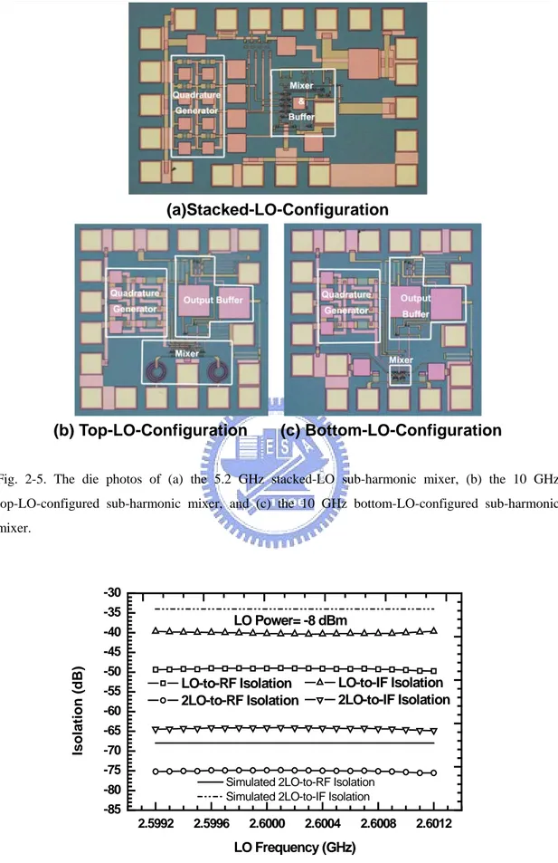
The die photo of the 5.004 GHz three-level stacked-LO sub-harmonic Gilbert mixer demonstrated in 2um GaInP/GaAs HBT is shown in Fig. 2-5(a). The LO and IF frequencies are 2.6 GHz and 400 KHz. The emitter areas of the GaInP/GaAs HBTs are 2um x 6um for the mixer core and 3um x 9um for the output buffer. The DC power supply is 3.3 V and the current consumption is only 4 mA including the output
buffer. The die size including probing pads is 1 x 1.5 mm2.
The die photos of the 10 GHz top-LO-configured and bottom-LO-configured mixers using the same technology are shown in Fig. 2-5(b) and Fig. 2-5(c), respectively. The LO and IF frequencies are 5 GHz and 100 MHz. Their die sizes
including probing pads are both 1 x 1 mm2. The chip sizes of the leveled-LO
sub-harmonic mixers can be shrunk because of the smaller RC values of the polyphase filter in higher frequencies. As shown in Fig. 2-5(b) and Fig. 2-5(c), there are two DC blocking capacitors of 8.2 pF. The core current of the top-LO-configuration mixer and the bottom-LO-configuration mixer are 2 mA and 0.8 mA, respectively. The circuit topology of the bottom-LO-configured mixer is the simplest and thus the DC current can be reduced.
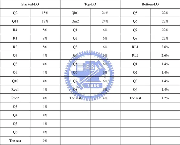
An off-chip 180 degrees hybrid and a pair of phase shifters are used to keep the phase accuracy; as a result, the intrinsic performance of the port-to-port isolation in a fully balanced Gilbert mixer is maintained. As shown in Fig. 2-6, the measured LO-to-IF, LO-to-RF, and 2LO-to-IF isolations are better than -40 dB, -50 dB, and -64 dB for the LO frequencies from 2.5992GHz to 2.6012 GHz. The 2LO leakage appearing at the RF port is directly measured by the spectrum analyzer [3]. The measured 2LO-to-RF leakage power is less than -83 dBm when the LO input power equals -8 dBm and the LO frequency is 2.6 GHz. The experimental result shows that the stacked-LO sub-harmonic topology and the GaAs semi-insulating substrate effectively reduce the 2LO-to-RF leakages. For comparison, the simulated 2LO-to-RF and 2LO-to-IF isolation are also plot.
(a)Stacked-LO-Configuration
(b) Top-LO-Configuration (c) Bottom-LO-Configuration
Fig. 2-5. The die photos of (a) the 5.2 GHz stacked-LO sub-harmonic mixer, (b) the 10 GHz top-LO-configured sub-harmonic mixer, and (c) the 10 GHz bottom-LO-configured sub-harmonic mixer. 2.5992 2.5996 2.6000 2.6004 2.6008 2.6012 -85 -80 -75 -70 -65 -60 -55 -50 -45 -40 -35 -30
Simulated 2LO-to-RF Isolation Simulated 2LO-to-IF Isolation
LO-to-IF Isolation 2LO-to-IF Isolation LO-to-RF Isolation 2LO-to-RF Isolation Isolation ( d B) LO Frequency (GHz) LO Power= -8 dBm
Fig. 2-6. The measured andsimulated LO-to-IF, 2LO-to-IF, LO-to-RF, and 2LO-to-RF isolations as a function of the LO frequency for the stacked-LO sub-harmonic mixers.
Figure 2-7 illustrates the LO-to-IF, 2LO-to-IF, LO-to-RF and 2LO-to-RF isolations as a function of LO frequency for the leveled-LO sub-harmonic mixers. The top-LO-configured mixer has -32 dB LO-to-RF isolation, -59 dB 2LO-to-RF isolation, -32 dB LO-to-IF isolation, and -46 dB 2LO-to-IF isolation, while the bottom-LO-configured counterpart has the -23 dB LO-to-RF isolation, -32 dB 2LO-to-RF isolation, -35 dB LO-to-IF isolation, and -48 dB 2LO-to-IF isolation.
The 2LO-to-RF isolation of the top-LO-configured mixer is better. The LO-to-RF isolation can be used to indicate the self-mixing problem for the CMOS passive mixer. Compared with previous literatures, the measured performance of the 2LO-to-RF isolations of the stacked-LO sub-harmonic mixers in our work is second to none when the RF frequency is around 5 GHz, as shown in the table 2-1.
4.85 4.90 4.95 5.00 5.05 5.10 5.15 -80 -70 -60 -50 -40 -30 -20 -10 LO Power= 15 dBm LO-to-IF(Bottom) 2LO-to-IF(Bottom) LO-to-RF(Bottom) 2LO-to-RF(Bottom) Isolation (dB) LO Frequency (GHz) LO-to-IF(Top) 2LO-to-IF(Top) LO-to-RF(Top) 2LO-to-RF(Top)
Fig. 2-7. The measured LO-to-IF, 2LO-to-IF, LO-to-RF, and 2LO-to-RF isolations as a function of LO frequency for the top-LO-configured and bottom-LO-configured sub-harmonic mixers.
The measured RF-to-IF isolation of the stacked-LO sub-harmonic mixer is -36 dB when the RF frequency is 5.2004 GHz. The RF-to-IF isolations of the top-LO and the bottom-LO sub-harmonic mixers as a function of RF frequency are shown in Fig. 2-8. The bottom-LO-configured mixer has better RF-to-IF isolation than the top-LO-configured one does.
Table 2-1: The 2LO-to-RF Isolations of Active Gilbert Sub-Harmonic Mixers 2LO-to-RF Isolation (dB) RF frequency (GHz) Die Size (mm2) Power Consumption (mW) Technology Stacked-LO 75 5.2 2 13.2 2um GaInP/GaAs HBT Top-LO 59 10 1 10 2um GaInP/GaAs HBT Bottom-LO 32 10 1 4 2um GaInP/GaAs HBT
Ref[3] 70 2 1.92 9.24 0.5um SiGe
HBT
Ref[20] 50 5-6 4.14 16.5 0.5um SiGe
HBT
Ref[39] 64 5 1.8 72 0.13um
CMOS
Ref[41] 35 5-6 0.7 47.5 0.5um SiGe
HBT 9.6 9.7 9.8 9.9 10.0 10.1 10.2 10.3 10.4 10.5 -70 -60 -50 -40 -30 -20 -10 RF -to-I F I s olati o n (dB) RF Frequency (GHz) RF-to-IF(TopLO) RF-to-IF(BottomLO) Simulated RF-to-IF(TopLO) Simulated RF-to-IF(BottomLO)
Fig. 2-8. The measured and simulated RF-to-IF isolations as a function of RF frequency of the top-LO-configured and bottom-LO-configured sub-harmonic mixers.
Figure 2-9 shows the measured conversion gain as a function of the LO power of all the sub-harmonic mixers. The conversion gain of the stacked-LO sub-harmonic mixer is 14.5 dB when LO power is larger than -10 dBm. As shown in Fig. 2-9, both leveled-LO sub-harmonic mixers require very large LO pumping powers. Compared with the stacked-LO structure, the LO pumping power of the leveled-LO mixer has to be 12 dBm for the optimal conversion gain while the stacked-LO structure only requires -9 dBm. -15 -10 -5 0 5 10 15 -8 -4 0 4 8 12 16 Simulated (Stack) Simulated (Top) Simulated (Bottom) Stacked-LO Mixer Convers ion Ga in (dB) LO Power (dBm) Top-Levled-LO Mixer Bottom-Levled-LO Mixer
Fig. 2-9. The measured andsimulated conversion gain as a function of the LO power of the stacked-LO, and leveled-LO mixers.
As discussed in the section previously, the leveled-LO mixer inevitably needs more LO pumping powers for the LO current fully switching, and the reason is that the leveled-LO mixer operates using the transistor second-harmonic currents. The leveled-LO cell requires extra 10 dBm LO power to perform the current commutation as analyzed previously. In addition, the loss of the polyphase filter used in the stacked-LO mixer is 2.4 dB while that of the leveled-LO mixer is about 6.5 dB according to our simulation. The measurement result is closed to our analysis as the polyphase loss is considered.
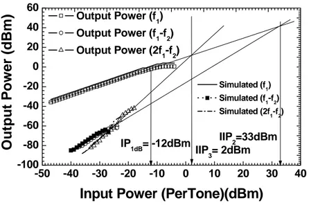
As shown in Fig. 2-10, the measured IP1dB, IIP3 and IIP2 performances of the 5.2