Anisotropy of light extraction from two-dimensional photonic crystal light-emitting
diodes
Chun-Feng Lai, H. C. Kuo, C. H. Chao, H. T. Hsueh, J.-F. T. Wang, W. Y. Yeh, and J. Y. Chi
Citation: Applied Physics Letters 91, 123117 (2007); doi: 10.1063/1.2789399
View online: http://dx.doi.org/10.1063/1.2789399
View Table of Contents: http://scitation.aip.org/content/aip/journal/apl/91/12?ver=pdfcov Published by the AIP Publishing
Articles you may be interested in
Light extraction from GaN-based light emitting diode structures with a noninvasive two-dimensional photonic crystal
Appl. Phys. Lett. 94, 023101 (2009); 10.1063/1.3067837
Enhanced light extraction from GaN-based green light-emitting diode with photonic crystal Appl. Phys. Lett. 91, 181109 (2007); 10.1063/1.2804005
Fabrication of two-dimensional photonic crystal patterns on GaN-based light-emitting diodes using thermally curable monomer-based nanoimprint lithography
Appl. Phys. Lett. 91, 091106 (2007); 10.1063/1.2776980
Enhanced light extraction from GaN-based light-emitting diodes with holographically generated two-dimensional photonic crystal patterns
Appl. Phys. Lett. 87, 203508 (2005); 10.1063/1.2132073
Efficiency enhancement in a light-emitting diode with a two-dimensional surface grating photonic crystal Appl. Phys. Lett. 84, 457 (2004); 10.1063/1.1644033
This article is copyrighted as indicated in the article. Reuse of AIP content is subject to the terms at: http://scitation.aip.org/termsconditions. Downloaded to IP: 140.113.38.11 On: Thu, 01 May 2014 00:07:32
Anisotropy of light extraction from two-dimensional photonic
crystal light-emitting diodes
Chun-Feng Lai and H. C. Kuoa兲
Department of Photonics and Institute of Electro-Optical Engineering, National Chiao-Tung University, Hsinchu, 300 Taiwan, Republic of China
C. H. Chao, H. T. Hsueh, J.-F. T. Wang, W. Y. Yeh, and J. Y. Chi
Electronics and Opto-Electronics Research Laboratories, Industrial Technology Research Institute, Hsinchu, 310 Taiwan, Republic of China
共Received 8 August 2007; accepted 4 September 2007; published online 20 September 2007兲 Anisotropic light extraction of photonic crystal 共PhC兲 light-emitting diodes in the azimuthal direction has been investigated with an annular structure of triangular PhC lattice. The optical images of the photoluminescence light extraction are obtained with laser excitation. For increasing lattice constant, sixfold symmetric patterns with varying numbers of petals in multiples of six are observed and analyzed. A map of the anisotropy for various lattice constants and numerical apertures is constructed. Several features of light propagations associated with the PhC are observed including the focusing and collimating behaviors. © 2007 American Institute of Physics.
关DOI:10.1063/1.2789399兴
Recently, photonic crystal 共PhC兲 has attracted a great deal of attention for the possibility to improve the extraction efficiency of light-emitting diodes 共LEDs兲.1–6 To optimize the device performance for a specific system, detailed knowl-edge of the light extraction, especially the angular distribu-tion, is required. Angular variations of light extraction in the zenith共vertical兲 direction have been investigated.7However, the angular distribution in the azimuthal共in-plane兲 direction has not been examined in detail.
In this paper, we present the direct imaging of the in-plane angular distribution of the extracted light using a spe-cially designed structure. A map of the anisotropy for various lattice constants and numerical apertures is constructed. Sev-eral features particular to the PhC properties have also been directly observed. These results can be used for the device optimization to take full advantage of the PhC.
The GaN epitaxial structure used for the present study was grown by metal-organic chemical vapor deposition, con-sisting of a 1-m-thick GaN buffer on a c-sapphire substrate, a 2m bottom n-GaN layer, a 100 nm InGaN / GaN multiple quantum well 共MQW兲 region, and a 130-nm-thick top
p-GaN current spreading layer, as shown in Fig. 1共a兲. The annular region of triangular PhC with an inner/outer diam-eter of 100/ 200m was patterned by electron-beam lithog-raphy. Holes were then etched into the top p-GaN layer using inductively coupled plasma dry etching to a depth t = 120 nm. The orientation of the triangular PhC is fixed in space and the ratio of hole diameter d to lattice constant a is also fixed to 0.6 to provide the consistent band structure.
After fabrication, the wafer is examined with a micro-photoluminescence 共-PL兲 system. A 325 nm He–Cd laser beam normally incidents into the central area of the ring and excites the wavelength=470 nm PL light in the MQW ac-tive region. The laser power used is about 3.2 mW and fo-cused to a spot of about 5m. A 15⫻ objective with nu-merical aperture共NA兲 of 0.32 is used to collect the on-axis emission signal from the sample and formed a
high-resolution image with a digital charge-coupled device共CCD兲 camera after filtering out the laser light.
Figure2shows the CCD images for samples with lattice constants a of 300, 450, 600, and 750 nm corresponding to
a / of 0.63, 0.96, 1.33, and 1.59, respectively. The bright
region that appeared in the center of all images is due to the unguided PL light. The petals in the PhC regions are due to the guided light that travel to the surrounding PhC region and get extracted. It can be seen that the angular distribution of the extracted light is strongly anisotropic. As a / in-creases, the increasing number of petals in multiples of six appears in a sixfold rotational symmetric pattern, indicating for certain directions, that stronger extraction with a focusing behavior is observed.
The observed anisotropy in Fig. 2 may be caused by either the coupling into the PhC region, which has been re-ported before,8 or by the diffraction of the light after cou-pling into the PhC. According to our finite-difference time domain 共FDTD兲 simulation, a coupling anisotropy of only ⬍5% are expected from the present shallow etch structure and high a / ⬎0.6. Therefore, the observed anisotropy is primarily due to the diffraction of the guided PL light of the PhC lattice into air and picked up by the microscope objec-tive.
The anisotropy due to diffraction can be explained by considering the Ewald construction in the reciprocal lattice. For simplicity, PhC is treated as a two-dimensional in an overall three-dimensional structure as is commonly done.7 Figure 3 shows the projection of the Ewald sphere on the waveguiding plane. The three circles in the figure correspond to the waveguide mode circle共blue dash line兲 with radius k = 2n/, where n is the effective refractive index of the guided wave, the air disk 共red solid line兲, with radius k0
= 2/, and the inner circle 共green solid line兲 corresponds to NA= sin, where is the acceptance angle for the optics used for the observation. The in-plane component of the re-sultant wavevector can couple to the reciprocal lattice vec-tors. If the resultant vector falls inside the air circle, the diffracted light can escape into air. However, to be picked up
a兲Electronic mail: [email protected]
APPLIED PHYSICS LETTERS 91, 123117共2007兲
0003-6951/2007/91共12兲/123117/3/$23.00 91, 123117-1 © 2007 American Institute of Physics
This article is copyrighted as indicated in the article. Reuse of AIP content is subject to the terms at: http://scitation.aip.org/termsconditions. Downloaded to IP: 140.113.38.11 On: Thu, 01 May 2014 00:07:32
with the objective lens, the diffracted light must fall within the NA circle. Using Ewald construction, this rule becomes simply to determine whether a reciprocal lattice point ap-pears inside the particular circles. This simple rule provides an explanation of the observed pattern of light extraction. It can also be used to define the conditions for observing of varying numbers of petals as a function of NA.
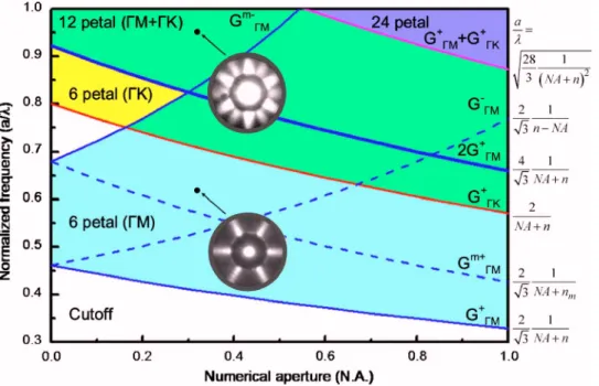
Figure4shows the boundary separating the regions with different numbers of petals along with our observations with NA= 0.32 and a /=0.63. As lattice constant increases above cutoff 共line G⌫-M+ in Fig. 4兲, light propagation in the ⌫-M
direction will start to be extracted 关Fig. 3共a兲兴. As a/ in-creases, the resultant wavevector after coupling to G⌫-Mfalls inside the NA circle关Fig.3共b兲兴. However, the opposite is true in the⌫-K direction 关Fig.3共c兲兴. Therefore, a pattern with six
petals pointing to the ⌫-M direction is observed. As a/ increases further, the resultant wavevector after coupling to
G⌫-M may fall short of the NA circle and will not be ob-served. Figure3共a兲关Fig.3共b兲兴 illustrates the situation when
the reciprocal points almost start to appear共disappear兲 inside the NA circle. Thus there is a range of a / that the resultant wavevector can fall into the NA circle in a particular direc-tion. This is represented as solid and dashed lines marked as
G⌫-M+ and G⌫-M− in Fig.4.
Since the the present thick epitaxial layer of 3.3m, the waveguiding is multimode. Every waveguiding mode can couple with the reciprocal vectors to form two lines in the same fashion described above. When plotted on the map, these multimodes will appear as a band of lines. For clarity, only the first and the last modes with mode number m are shown in Fig. 4. The two outmost lines, G⌫-M+ and G⌫-Mm− , define the boundary of the possible a /’s for all the modes that can fall into NA circle after coupling to G⌫-M.
For still larger lattice constant of a /⬎2/n, coupling to the second nearest vector G⌫-K becomes possible and six more petals appear representing six equivalent ⌫-K direc-tions. The boundary for all the coupling to G⌫-K can be drawn in the same way as above and is indicated by G⌫-K+ and
G⌫-K− 共fall outside Fig. 4, not shown兲. In the overlap of the
two regions, 12 petals will be obtained, pointing alternately to the⌫-M and ⌫-K directions. For even larger lattice con-stants, coupling to the third and fourth nearest lattice points, with the vector length two times the G⌫-M 共line 2G⌫-M+ 兲 and
G⌫-M− + G⌫-K共line G⌫-M+ + G⌫-K+ 兲 is possible and the number of petals increases to 24. Also there are regions where no dif-FIG. 1. 共Color online兲 共a兲 Annual structure and the light generation, waveguiding, and extraction in the present structure, 共b兲 Scanning elec-tron microscope micrograph of the PhC region.
FIG. 2. CCD images for various lattice constants of共a兲 300, 共b兲 450, 共c兲 600, and共d兲 750 nm. The central bright region in all the photos is due to the unguided PL light excited by the focused laser beam impinging normally in the center.
FIG. 3. 共Color online兲 Ewald construction for 共a兲 the resultant wavevetor just entering the NA circle, 共b兲 coupling in the G⌫-M direction for a = 300 nm showing the resultant wavevetor almost leaving the NA circle, and 共c兲 coupling in the G⌫-Kdirection for a = 300 nm showing no light can
es-cape into the NA.
123117-2 Lai et al. Appl. Phys. Lett. 91, 123117共2007兲
This article is copyrighted as indicated in the article. Reuse of AIP content is subject to the terms at: http://scitation.aip.org/termsconditions. Downloaded to IP: 140.113.38.11 On: Thu, 01 May 2014 00:07:32
fraction appears, corresponding to the light escaping the sur-face with angles larger than NA. The formulas for the bound-ary between regions with different numbers of petals can be readily derived and are shown in Fig.4.
It is also observed that the interference fringes are super-imposed on the patterns, as shown in Fig.2共a兲. The spacing of the fringes stays the same for all propagation directions and lattice constants. The origin of the fringes is most likely due to the multimode interferences 共MMIs兲 of the modes traveling in the waveguide formed by the epitaxial film on top of the sapphire. For a quantitative comparison, the spac-ing due to MMI are calculated with the formula s = 4neW2/共N0兲.9Using an epithickness W of 3.23m, a
to-tal mode number N of 25 modes supported by the waveguide before the leakage into the sapphire substrate, and the effec-tive index ne of 2.5, the spacing is determined to be about
9m, or 9.8m with the Goose-Hahnchen correction. This value is reasonably close to the measured fringe spacing of 10.4m, considering the inaccuracy of the parameters in the formula.
In addition to the observed number of petals, the shape of the individual petals is worth commenting on: The petals inside the annular regions are convergent in shape, instead of the expected divergent shape. Such a shape may be due to the dispersion of the band structure. For the 12-petals pattern shown in Fig.2共b兲, it is seen that the focusing is stronger in the⌫-M directions than the ⌫-K directions which may reflect the different dispersion properties of the two directions. In addition to the anisotropy, the emitted light are polarized with a TE/TM ratio larger than 10. The intensity of the ex-tracted light decreases with a decay length of 70– 90m, depending on the orientation and the holes size; this value is
in the same range of that reported in Ref.7. The discussion of these details will be reported elsewhere.
In conclusion, optical images of the anisotropy in the azimuthal direction of GaN PhC LEDs are obtained using annular structure with triangular lattice. The presented imag-ing approach can be used to study the propagation of light in the PhC slabs and provides information important for design-ing LED and other photonic devices.
The authors gratefully acknowledge Dr. S. C. Wang at National Chiao-Tung University 共NCTU兲 and Y. S. Liu at National Tsing-Hua University共NTHU兲 in Taiwan for their technical support. This work is supported by the National Nanotechnology Program of Taiwan, R.O.C., and the MOE ATU program and, in part, by the National Science Council of the Republic of China under Contract Nos. NSC 2120-M-009-008, NSC 2752-E-009-007-PAE, and NSC 95-2221-E-009-282.
1E. F. Schubert, Light-Emitting Diodes共Cambridge University Press,
Cam-bridge, 2003兲.
2H. Ichikawa and T. Baba, Appl. Phys. Lett. 84, 457共2004兲.
3T. N. Oder, K. H. Kim, J. Y. Lin, and H. X. Jiang, Appl. Phys. Lett. 84,
466共2004兲.
4J. J. Wierer, M. R. Krames, J. E. Epler, N. F. Gardner, and M. G. Craford,
Appl. Phys. Lett. 84, 3885共2004兲.
5J. Shakya, K. H. Kim, J. Y. Lin, and H. X. Jiang, Appl. Phys. Lett. 85, 142
共2004兲.
6C. H. Chao, S. L. Chuang, and T. L. Wu, Appl. Phys. Lett. 89, 091116
共2006兲.
7A. David, C. Meier, R. Sharma, F. S. Diana, S. P. DenBaars, E. Hu, S.
Nakamura, and C. Weisbuch, Appl. Phys. Lett. 87, 101107共2005兲.
8A. Martinez and J. Marti, Phys. Rev. B 71, 235115共2005兲. 9R. Ulrich and G. Ankele, Appl. Phys. Lett. 27, 337共1975兲.
FIG. 4. 共Color online兲 Map for the arithmuzal anisotropy of the triangular lattice as a function of NA. The re-gions of various petals are shown with different colors. The directions of the petals are shown in parentheses. The “⫹” and “⫺” signs indicate the lower and upper boundaries for the regions.
123117-3 Lai et al. Appl. Phys. Lett. 91, 123117共2007兲
This article is copyrighted as indicated in the article. Reuse of AIP content is subject to the terms at: http://scitation.aip.org/termsconditions. Downloaded to IP: 140.113.38.11 On: Thu, 01 May 2014 00:07:32