Effect of phosphorus dopant on photoluminescence and field-emission characteristics
of Mg 0.1 Zn 0.9 O nanowires
Chia Ying Lee, Tseung Yuen Tseng, Seu Yi Li, and Pang Lin
Citation: Journal of Applied Physics 99, 024303 (2006); doi: 10.1063/1.2161420 View online: http://dx.doi.org/10.1063/1.2161420
View Table of Contents: http://scitation.aip.org/content/aip/journal/jap/99/2?ver=pdfcov Published by the AIP Publishing
Articles you may be interested in
Photoluminescence and built-in electric field in Zn O Mg 0.1 Zn 0.9 O quantum wells Appl. Phys. Lett. 90, 132113 (2007); 10.1063/1.2716367
Electron field-emission properties of Ag – Si O 2 nanocomposite layers J. Vac. Sci. Technol. B 24, 958 (2006); 10.1116/1.2165669
Influence of Zr O 2 addition on the microstructure and discharge properties of Mg–Zr–O protective layers in alternating current plasma display panels
J. Appl. Phys. 98, 043304 (2005); 10.1063/1.2009077
Realization of Mg ( x = 0.15 ) Zn ( 1 x = 0.85 ) O -based metal-semiconductor-metal UV detector on quartz and sapphire
J. Vac. Sci. Technol. A 23, 982 (2005); 10.1116/1.1913677 Refractive indices of cubic-phase Mg x Zn 1 x O thin-film alloys J. Appl. Phys. 97, 023515 (2005); 10.1063/1.1821633
Effect of phosphorus dopant on photoluminescence and field-emission
characteristics of Mg
0.1Zn
0.9O nanowires
Chia Ying Lee
Department of Electronics Engineering and Institute of Electronics, National Chiao Tung University, Hsinchu 300, Taiwan
Tseung Yuen Tsenga兲
Department of Electronics Engineering and Institute of Electronics, National Chiao Tung University, Hsinchu 300, Taiwan and Department of Materials and Mineral Resources Engineering,
National Taipei University of Technology, Taipei 106, Taiwan Seu Yi Li and Pang Lin
Institute of Materials Science and Engineering, National Chiao Tung University, Hsinchu 300, Taiwan 共Received 24 May 2005; accepted 29 November 2005; published online 20 January 2006兲 The photoluminescence and field-emission properties of Mg0.1Zn0.9O nanowires 共MZO NWs兲
hydrothermally grown on the p-type silicon共100兲 substrates with and without phosphorus dopant were investigated in this study. Parts of MZO NWs were treated with PH3 plasma to form
phosphorus-doped MZO NWs共PMZO NWs兲. The MZO and PMZO are wurtzite single crystals, and the surface morphologies of MZO NWs are identical to those of PMZO NWs with an average diameter of 50 nm and a length of 500 nm. The direct band gaps and emitted ultraviolet photoluminescences of the MZO and PMZO NWs are 3.41 eV and 403.8 nm and 3.56 eV and 385.4 nm, respectively. The MZO NWs grown on Si substrates have an emission threshold electric field of 1.8 V /m共current density of 1.0 mA/cm2兲 and a field enhancement factor,, of 3048 while the PMZO NWs show enhanced properties with a threshold electric field of 1.5 V /m and a value of 3054. These field-emission properties are also enhanced by illumination, which reveals that the emission behavior is affected by the surface charge state. Therefore, it is suggested that the band structure of MZO NWs has been modulated by phosphorus incorporation. © 2006 American
Institute of Physics.关DOI:10.1063/1.2161420兴
I. INTRODUCTION
Recently, one-dimensional nanowires共NWs兲 have been extensively studied for potential applications to photonic, electro-optical, and electronic devices because of their unique physical and chemical properties. There are various methods to synthesize the NWs; however, the hydrothermal process has several advantages over other growth processes such as catalyst-free growth, low cost, large area uniform production, environmental friendliness, and low reaction temperature to integrate into the microelectronics and plastic electronics. The NWs with sharp tips are suitable structures for cold cathode field-emission device application. It has been reported that the emission characteristics of Si NWs depend on the doping type共n and p types兲.1–3However, the field-emission properties of other NWs with various dopants are still unclear.
Zinc oxide共ZnO兲 is an attractive material for electronic and electro-optical devices, such as the ultraviolet共UV兲 laser device,phosphor, transparent conducting films for solar cell, and flat panel display, because of its wide band gap共3.4 eV兲 and large exciton binding energy 共60 meV兲.4–6 Current trends in developing ZnO-based optoelectronic devices are focused on synthesizing reliable n-type and p-type ZnO.7,8 But, it was difficult to fabricate reproducible p-type ZnO due
to self-compensation and low solubility of dopants.9 Re-cently, Norton and co-workers have reported that the P0.02Mg0.1Zn0.9O film showed stable p-type behavior by add-ing Mg and P together—Mg dopant to increase the band gap and P dopant to introduce the acceptor level.10,11
In this work, the Mg0.1Zn0.9O 共MZO兲 NWs are fabri-cated on p-type 关B doped, 1−10 ⍀ cm兴 Si substrates by the hydrothermal method. The P ions were incorporated into part of the MZO NWs to form phosphorus-doped MZO NWs 共PMZO NWs兲 by using plasma treatment. The crystal struc-ture, chemical composition, photoluminescence, and field-emission characteristics of MZO and PMZO NWs on the
p-type Si 共100兲 substrates were examined. The effect of
phosphorus dopant on the properties of MZO NWs was also studied.
II. EXPERIMENT
Before deposition, the p-type Si substrates were cleaned by Radio Corporation of America 共RCA兲 clean process to remove native silicon oxide on the substrate surface. Ultra-thin ZnO seeding film 共⬃70 Å兲 was deposited on the Si substrate by rf-sputtering 共13.56 MHz兲 method under Ar sputtering gas at 20 mTorr. Then, the coated Si substrate was put into an aqueous solution 共Milli Q, 18.2 M⍀ cm兲 of zinc nitrate hexahydrate 共Zn共NO3兲2· 6H2O , 0.01M兲,
magnesium nitrate hexahydrate 共Mg共NO3兲2· 6H2O , 0.06M兲,
and diethylenetriamine 共HMTA, C6H12N4兲 with a pH value
a兲Author to whom correspondence should be addressed; electronic mail:
0021-8979/2006/99共2兲/024303/6/$23.00 99, 024303-1 © 2006 American Institute of Physics [This article is copyrighted as indicated in the article. Reuse of AIP content is subject to the terms at: http://scitation.aip.org/termsconditions. Downloaded to ] IP:
of 7.2 in a sealed vessel at 75 °C for 1 h. After this hydro-thermal reaction, the MZO NWs can be formed on the Si substrate and the color of the product was gray. The micro-structure and properties of the synthesized MZO NWs that have been cleaned with deionized共DI兲 water and dried in the vacuum oven at room temperature for 5 h were investigated. To fabricate the PMZO NWs, the MZO NWs were exposed to PH3 plasma for 120 s. The plasma treatment was carried
out in an inductively coupled plasma共ICP兲 reactor using a 3 kW ICP power supply. The processing conditions were under 10 mTorr working pressure, 200 W ICP, 200 °C reaction temperature, and both Ar 共99.5%兲 and PH3 共99.5%兲 with
100 cm3/ min flow rate. Then, these NWs were rapid ther-mally annealed 共RTA兲 at 300 °C for 30 min in the oxygen atmosphere. The crystal structure of the NWs was examined by x-ray diffraction共XRD兲 共MAC Science, MXP18, Japan兲. The surface morphologies of the NWs were observed by field-emission scanning electron microscopy 共FESEM兲 共Hi-tachi S-4700I, Japan兲 and high-resolution transmission elec-tron microscopy 共HRTEM兲 共Philips tecani–20兲. The chemi-cal composition of the NWs was analyzed by x-ray photoelectron spectroscopy共XPS兲 共VG Scientific ESCALAB 250兲. Room-temperature optical properties characterizations were performed by UV-visible共UV-VIS兲 spectrometer Hita-chi 557, Japan兲 and photoluminescence analyzer 共PL, HitaHita-chi F–4500, Japan兲 with Xe lamp as an excitation source 共325 nm兲. The conducting behaviors of MZO and PMZO were characterized by the Hall-effect measurements共HL500PC兲 at a magnetic-field strength of 0.3 T at room temperature. The samples used for this measurement were bulk materials, which have the same chemical compositions as the NWs. The field-emission characteristics of the NWs were measured by Keithley 237 source-measure unit in a vacuum chamber at a pressure of 1⫻10−6Torr at room temperature. In the field-emission measurement, a tungsten anode with an area of 7.0⫻10−3cm2was placed at a distance of 350m from tips
of the NWs, which can be adjusted by a precision screw meter with an accuracy of ±0.1m.
III. RESULTS AND DISCUSSION
The typical FESEM images which illustrate the surface morphologies of MZO and PMZO NWs on p-type Si sub-strates are shown in Fig. 1. It is indicated that the randomly oriented MZO NWs have an average diameter of 50 nm, an average length of 0.5m, and a number density of 3.4 ⫻1010cm−2. These NWs are nonvertical and randomly
dis-tributed over the polycrystalline ZnO seeding film and ex-hibit homogeneous morphologies with hexagonal columnar shape. The surface morphologies of PMZO NWs关Fig. 1共b兲兴 including shape, diameter, length, and number density are identical to those of MZO NWs. Thus, the surface morpholo-gies of the MZO NWs remain unchanged after the PH3
plasma treatment.
The crystal structure and phase of the NWs were deter-mined by XRD. Figure 2 depicts the XRD patterns of MZO and PMZO NWs grown on the p-type Si substrates, respec-tively, and the inset is the enlarged XRD patterns of peak 共002兲 of the NWs with 2from 34° to 35°. The XRD peak at 33.06° is caused by the Si substrate, and three main diffrac-tion peaks are indexed as 共100兲, 共002兲, and 共110兲 of the wurtzite structure, respectively. Thus, single phase MZO and PMZO NWs with the wurtzite structure were synthesized by the hydrothermal method. The lattice constants and corre-sponding cell volumes共3
冑
3a2c / 2兲 of MZO and PMZO NWscan be calculated from their XRD patterns. The c-axis lengths calculated from the 共002兲 peak of MZO and PMZO are 5.192 and 5.198 Å, respectively; a-axis length calculated from the 共100兲 peak is 3.241 Å for both NWs, and the cell volumes are 141.69 and 141.86 Å3, respectively. After the P
plasma treatment, the PMZO NWs retain the crystal structure of wurtzite and no other impurities appear but have a small change in the c-axis length and slight increase in cell vol-ume. The variation of the c-lattice constant may be due to the P plasma implanting perpendicularly to the substrate. Such a P implantation along the共002兲 direction of MZO leads to an increase in the c-axis parameter. The addition of P to MZO forms a solid solution with the wurtzite structure; a possible reaction is
P
→ 共Mg,Zn兲OPO
⬘
+ V共Mg,Zn兲⬙
, 共1兲 where PO⬘
means P3− substituted for O2− site and V共Mg,Zn兲
⬙
indicates a vacancy formed at a Zn2+ or Mg2+ site in the
lattice of the MZO NWs. It is suggested that a P3− ion is
substituted for an O2− ion, which leads to a Zn vacancy for-mation. Therefore, the deviation of the lattice constants can be due to the P atoms incorporated in the NWs by plasma implantation and the different ionic radii between P3−共rP3− = 1.06 Å兲 and O2− 共r
O
2−= 0.73 Å兲. FIG. 1. Cross-section FESEM micrographs of 共a兲 MZO NWs, and 共b兲
PMZO NWs grown on Si substrates.
FIG. 2. XRD patterns of共a兲 MZO NWs and 共b兲 PMZO NWs grown on Si substrates. The inset is the enlarged patterns with 2from 34° to 35°.
024303-2 Lee et al. J. Appl. Phys. 99, 024303共2006兲
The typical HRTEM image of PMZO NWs and corre-sponding selected area electron diffraction 共SAED兲 are shown in Fig. 3, which illustrates the microstructural features of the PMZO NWs. The SAED pattern in the inset of Fig. 3 can be indexed to the reflection of single-crystalline PMZO hexagonal structure, and its lattice constants are a = b = 3.241 Å and c = 5.198 Å, which are consistent with the XRD result. The SAED pattern indicates that the NWs grow in the关0002兴 direction with wurtzite structure, and the dis-tance between parallel 关0002兴 lattice fringes of the NWs is 5.198 Å. This pattern also depicts the single-crystalline struc-ture of the PMZO NWs. Moreover, the defects such as dis-locations and stacking fault were not observed in the PMZO NWs. For both the MZO and PMZO NWs, only the growth direction关0002兴 was found. It concludes that the MZO NWs can be doped with P by the plasma treatment but without damaging its crystal structure.
The chemical composition of the PMZO NWs was fur-ther analyzed by the XPS and the results are shown in Fig. 4. The XPS spectrum of PMZO NWs shows that there are fea-ture peaks corresponding to elements of Zn, Mg, P, O, C, and Si. Three strong peaks located at 530.8, 1024.4, and 1048.0 eV are, respectively, due to the O 共1s兲 and Zn 共2p3/2 and
2p1/2兲 binding energies for ZnO NWs, while three weak
peaks located at 49.6, 129.9, and 130.5 eV are due to the Mg 共2p兲 and P 共2p3/2 and 2p1/2兲 binding energies for Mg and P
incorporated in the NWs. The appearance of carbon at the peak of 263 eV results from the residual reactants adsorbed on the surface of the NWs, and the peak of Si was detected due to the Si substrate. Obviously, the dominant chemical composition of the NWs is ZnO and a little amount of Mg and P is incorporated into these NWs on the basis of the results of XPS measurement. With further detailed examina-tions, the chemical composition of these NWs is P0.02Mg0.1Zn0.9O.
Figure 5共a兲 shows the photoluminescence spectra of MZO and PMZO NWs excited by a Xe lamp共=325 nm兲 at
room temperature. It is indicated that MZO NWs emit lumi-nescences at 403.8 nm共3.07 eV兲, 451 nm 共2.75 eV兲, 465 nm 共2.67 eV兲, 495 nm 共2.51 eV兲, and 520 nm 共2.38 eV兲, respec-tively. The UV emission at 403.8 nm is caused by the band-edge emission of MZO. The luminescence at 451 nm was reported to be due to the Zn vacancy 共VZn
⬙
兲.12 The emission of 465 nm may be associated with the oxygen deficiency in these NWs formed in the growth environment of hydrother-mal process.13 The possible reactions that take place in the aqueous solution in such an environment are the following:共CH2兲6N4+ 10H2O→ NH4OH + 6HCHO, 共2兲
共Zn2+,Mg2+兲 + 2OH−→ 共Zn,Mg兲O + H
2O. 共3兲
The Zn2+ions are sufficient in this solution, but the OH−
ions are finite in the solution because hexamethylenetetra-mine 共HMTA兲 slowly releases OH−. Thus, oxygen is
ex-pected to be lacking in the NWs fabricated by the hydrother-mal method. This phenomenon also results in the deep-level14and singly ionized oxygen vacancies15 lumines-cences at 495 and 520 nm as shown in Fig. 5共a兲. On the other
FIG. 3. HRTEM micrograph of PMZO NWs. The inset is the corresponding SAED of the NWs.
FIG. 4.共a兲 XPS spectrum of PMZO NWs, 共b兲 Zn spectrum, 共c兲 O spectrum, 共d兲 Mg spectrum, and 共e兲 P spectrum.
hand, the PMZO NWs emit 385.4 nm 共3.22 eV兲, 412 nm 共3.02 eV兲, 451, 465, 480 nm 共2.58 eV兲, 495, and 520 nm luminescences. It is shown that the near band-edge emission peak shifts from 403.8 to 385.4 nm and a Stokes shift of 0.15 eV happens as the P was incorporated in the MZO NWs. Such a blueshift of optical band-to-band transitions was re-ported to be related to the Burstein-Moss effect.16The emis-sions at 412 and 480 nm may be associated with the nonsto-ichiometric oxide17 and ionized Zn vacancy 共VZn
⬘
兲 共Ref. 12兲 in the PMZO NWs. The UV emission of PMZO NWs is a little weaker than that of MZO NWs, while the emissions of PMZO NWs at 465, 495, and 520 nm caused by oxygen vacancies are much weaker than those of MZO NWs. It could be proposed that the P substitution causes the oxygen vacancies in PMZO to decrease and introduces an acceptor level leading to a decrease in electron concentration but an increase in hole concentration and finally PMZO NWs be-come p-type conduction, which can be further verified by the following the Hall-effect measurement. Room-temperature transmission spectra of MZO and PMZO NWs were re-corded by an UV-visible spectrometer. To realize the rela-tionship between the transmission spectra and the band gap, 共␣h兲1/2 is plotted as a function of photon energy 共h兲 as shown in Fig. 5共b兲. The absorption edge is used to determine the energy band gap共Eg兲 of the NWs. The band gap of MZONWs is 3.41 eV, and that increases to 3.56 eV for the PMZO NWs. Such an increase is attributed to the broadening effect18 occurring as the carriers feel different potentials for the different local concentrations of the substituting elements
in the crystal. Therefore, the band gap can be modulated by adding P content in the MZO NWs, which may be applied in various optoelectronic applications.
On the basis of the results of the Hall-effect measure-ment, the MZO bulk performs the n-type conduction with a resistivity of 1.1⍀ cm, Hall mobility of 10.2 cm2/ V s, and
carrier concentration of 5.8⫻1017cm3, while the PMZO one exhibits the p-type behavior with a resistivity of 4.3 ⫻10−1 ⍀ cm, Hall mobility of 15.8 cm2/ V s, and carrier
concentration of 9.2⫻1017cm3. Therefore, it can be ex-pected that the PMZO NWs also exhibit p-type conductivity due to the same composition between NWs and bulk mate-rials we measured.
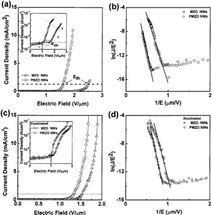
The field-emission characteristics of the MZO and PMZO NWs on the p-type Si 共100兲 substrate are shown in Fig. 6. As shown in Fig. 6共a兲, the turn-on electric field 共Eon, under the current density of 1.0A / cm2兲 and threshold elec-tric field 共Eth, under the current density of 1.0 mA/ cm2兲 of
MZO NWs are 1.3 and 1.9 V /m, respectively, while those of PMZO NWs are 1.0 and 1.5 V /m, respectively. The semilogarithmic plots of J-E field-emission characteristics shown in the inset of Fig. 6共a兲 further identify their emission properties. These plots can be divided into three parts: zero emission 共region 1兲, Fowler-Nordheim 共F-N兲 field emission 共region 2兲, and current saturation region 共region 3兲. The Eon
is defined as the electric field for which tunneling of PMZO NWs occurs and is 1.0 V /m which is lower than that of MZO NWs共1.3 V/m兲. Above Eon共region 2兲, the emission
current density abruptly increases and then saturates at the high electric-field region 共region 3兲. The current density emitted by MZO NWs is lower than that of PMZO NWs under the same electric field. A knee electric field, Eknee, is
defined as the demarcation point between F-N field-emission and current saturation regions. The Ekneeof MZO and PMZO
NWs, respectively, are 1.8 and 1.5 V /m. In this F-N tun-neling region, the better field-emission properties were ob-served for the PMZO as compared with MZO because the resistance of PMZO is smaller. This worse field-emission ability of MZO may be due to a potential barrier formed by the negative charge in the surface state of n-type emitters.1,2 Thus, the p-type PMZO NWs with lower surface state barrier perform the better field-emission properties. The MZO and PMZO NWs on p-type Si substrates perform at a saturation region at higher electric field共region 3兲 in the J-E plot. This saturation region exists due to the high resistance in the se-ries of semiconductor emitters.19 As shown in the inset of Fig. 6共a兲, the resistances in series of MZO and PMZO NWs are introduced to fit the J-E plot and the values of 93 and 62 k⍀ are obtained, respectively. The decreasing resistance in the series of PMZO NWs is attributed to a lower potential barrier formed by the positive charge in the surface state of
p-type PMZO emitters. Obviously, the P dopant can improve
the field-emission properties of MZO NWs on the p-type Si 共100兲 substrate. The PMZO NWs with the low threshold electric field and low resistance in series are suitable for the field-emission applications.
The corresponding F-N plots 关ln共J/E2兲 vs E−1兴 of the
MZO and PMZO NWs on the p-type Si共100兲 substrate are
FIG. 5. 共a兲 Photoluminescence 共PL兲 spectra of MZO and PMZO NWs. 共b兲 Tauc’s plots of MZO and PMZO NWs.
024303-4 Lee et al. J. Appl. Phys. 99, 024303共2006兲
depicted in Fig. 6共b兲, indicating that the measured field-emission characteristics fit the F-N relationship. The F-N re-lationship is as follows: J =A 2E2 exp
冉
− B3/2 E冊
, 共4兲where J is the current density, E the applied field,⌽ the work function of the ZnO 共5.37 eV兲,  the field enhancement factor, A = 1.56⫻10−10共A V−2eV兲, and B=6.83⫻103
共V eV−3/2m−1兲. The calculated  value of MZO NWs is
3048, and that of PMZO NWs is 3054. Therefore, the  value of PMZO NWs is close to that of MZO NWs. It is well known that the  depends on the geometry, structure, tip size, and number density of the emitters on the substrate. It is believed that the similar surface morphology and structure between PMZO and MZO NWs共Figs. 1–3兲 is the main rea-son for having nearly same values.
The photoenhanced field-emission properties of MZO and PMZO under a 30 W incandescent lamp irradiation are studied to demonstrate the influence of the illumination on the field emission. The Eon, Eth, Eknee, , and Rs values of
these NWs can be obtained from the slopes and fitting curves of the F-N plots and are listed in Table I. The Eonand Ethof
PMZO NWs under illumination decrease to 0.9 and 1.3 V /m, respectively, and its maximum current density increases to 72 mA/ cm2. As shown in the insert of Fig. 6共c兲, the calculated resistances in series of the MZO and PMZO NWs under illumination from the fitting are 72 and 45 k⍀, respectively, which are lower than those values without illu-mination. Thevalues of these two NWs under illumination calculated from the slopes of the F-N plots 关Fig. 6共d兲兴 are identical to those of the dark one. Therefore, it is demon-strated that the carriers in the MZO and PMZO NWs are excited during the illumination, leading to an increase in the emission current density and a reduction in the resistance in series, but unchanged structure and surface morphology after illumination lead to similar values.
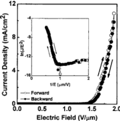
Figure 7 depicts the J-E curves and corresponding F-N plots with E from 0 to 1.95 V /m共forward sweep兲 and then back to 0 V /m 共backward sweep兲 of PMZO NWs grown on the p-type Si substrate. The two J-E curves are almost merged and no hysteresis behavior caused by adsorbates20is
FIG. 6. 共a兲 Field-emission J-E curves of MZO and PMZO NWs grown on p-type Si substrate. The inset is the semilogarithmic J-E plot and resistance in series fitting. 共b兲 The corresponding F-N 关ln共J/E2兲 vs E−1兴
plots of the NWs. 共c兲 Photoenhanced field-emission characteristics of MZO and PMZO NWs grown on Si substrates. The insert is the fitting of resistance in se-ries.共d兲 Corresponding F-N plots.
TABLE I. Eon, Eth, Eknee,, and Rsvalues of MZO NWs and PMZO NWs grown on the Si substrates with and without illumination.
MZO PMZO
Dark Illuminated Dark Illuminated
Eon共V/m兲 1.3 1.0 1.0 0.9
Eth共V/m兲 1.9 1.5 1.5 1.3
Eknee共V/m兲 1.8 1.6 1.5 1.4
 3048 3049 3054 3058
Rs共k⍀兲 93 72 62 45
observed in this measurement. Thus, it is demonstrated that the good field-emission performance 共low turn on electric field and high emission current density兲 of PMZO NWs is not caused by the adsorbates on the NWs but the intrinsic properties of the NWs.
IV. CONCLUSIONS
In summary, the single-crystalline MZO and PMZO NWs on the p-type Si 共100兲 substrates are synthesized by hydrothermal route. The structure and surface morphology of MZO NWs are similar to those of PMZO NWs. The average diameter of these two nanostructures is 50 nm and the length is 500 nm. Room-temperature transmission spectra illus-trated that the band gap of MZO NWs shifts from 3.41 to 3.56 eV, and the band-edge emission from 403.8 to 385.4 nm when the plasma implantation of P into them occurs to form PMZO NWs. Moreover, such PMZO NWs exhibit better field-emission properties including the lower threshold elec-tric field, lower resistance in series, and higher emission cur-rent density, in comparison with MZO NWs. The improved field-emission characteristic of PMZO is attributed to the changes in surface state of the nanostructure at both thresh-old voltage and F-N field-emission regions. The PMZO NWs with good field-emission properties are a suitable material
for flat display application. Moreover, the modulated band gap can be obtained with P doping but keep similar crystal structure, which may also be able to be applied for the future nanohomojunction ZnO optoelectronic and field-emission devices.
ACKNOWLEDGMENT
This work was supported by the National Science Coun-cil of R.O.C. under Contract No. NSC 93–2216–E–009–024.
1S. Johnson, A. Markwitz, M. Rudolphi, H. Baumann, S. P. Oei, B. K. Teo,
and W. I. Milne, Appl. Phys. Lett. 85, 3277共2004兲.
2T. Matsukawa, S. Kanemaru, K. Tokunaga, and J. Itoh, J. Vac. Sci.
Tech-nol. B 18, 1111共2000兲.
3S. Kanemuru, T. Hirano, H. Tanoue, and J. Itoh, Appl. Surf. Sci. 111, 218
共1997兲.
4S. Y. Li, P. Lin, C. Y. Lee, and T. Y. Tseng, J. Appl. Phys. 95, 3711共2004兲. 5A. Gupta and A. D. Compaan, Appl. Phys. Lett. 85, 684共2004兲. 6S. Fujihara, A. Suzuki, and T. Kimura, J. Appl. Phys. 94, 2411共2003兲. 7J. M. Bian, X. M. Li, C. Y. Zhang, W. D. Yu, and X. D. Gao, Appl. Phys.
Lett. 85, 4070共2004兲.
8K. Ip, Y. W. Heo, D. P. Norton, S. J. Pearton, J. R. LaRoche, and F. Ren,
Appl. Phys. Lett. 85, 1169共2004兲.
9S. B. Zhang, S. H. Wei, and Y. Yan, Physica B 302, 135共2001兲. 10Y. K. Kwon, Y. Li, Y. W. Heo, M. Jones, P. H. Holloway, D. P. Norton, Z.
V. Park, and S. Li, Appl. Phys. Lett. 84, 2685共2004兲.
11Y. W. Heo, Y. K. Kwon, Y. Li, S. J. Pearton, and D. P. Norton, Appl. Phys.
Lett. 84, 3474共2004兲.
12S. A. M. Lima, F. A. Sigoli, M. Jafelicci, Jr., and M. R. Davolos, Int. J.
Inorg. Mater. 3, 749共2001兲.
13Y. Du, W. L. Cai, C. M. Mo, J. Chen, L. D. Zhang, and X. G. Zhu, Appl.
Phys. Lett. 74, 2951共1999兲.
14J. Wang, G. Du, Y. Zhang, B. Zhao, X. Yang, and D. Liu, J. Cryst. Growth
263, 269共2004兲.
15K. Vanheuseden, W. L. Warren, C. H. Seager, D. R. Tallant, J. A. Voigt,
and B. E. Gnade, J. Appl. Phys. 79, 7983共1996兲.
16T. Makino, Y. Segawa, S. Yoshida, A. Tsukazaki, A. Ohtomo, and M.
Kawasaki, Appl. Phys. Lett. 85, 759共2004兲.
17S. S. Chang, S. O. Yoon, H. J. Park, and A. Sakai, Mater. Lett. 53, 432
共2002兲.
18R. D. Shannon, Acta Crystallogr., Sect. A: Cryst. Phys., Diffr., Theor. Gen.
Crystallogr. 32, 145共1976兲.
19S. Y. Li, P. Lin, C. Y. Lee, T. Y. Tseng, and C. J. Huang, J. Phys. D 37,
2274共2004兲
20H. Z. Zhang, R. M. Wang, and Y. W. Zhu, J. Appl. Phys. 96, 624共2004兲.
FIG. 7. Field-emission J-E curves of PMZO NWs with forward and back-ward sweeps. The inset depicts the corresponding F-N plot.
024303-6 Lee et al. J. Appl. Phys. 99, 024303共2006兲