國
立
交
通
大
學
電子工程學系 電子研究所
博 士 論 文
三 維 的 半 極 性 { ̅ } 平 面 與 非 極 性 { ̅ } 平 面
核 殼 狀 氮 化 銦 鎵 / 氮 化 鎵 多 重 晶 面 量 子 井
光
電
元
件
之
製
作
與
特
性
研
究
Fabrication and Characterization of Three Dimensional Core-shell InGaN/GaN
Multi-Facet Qunatum Wells Optoelectronics Devices on
Semipolar {10-11} and Nonpolar {10-10} Plane
研 究 生:張哲榮
指導教授:張俊彥 教授
三維的半極性
{ ̅ }
平面與非極性
{ ̅ }
平面核殼狀
氮化銦鎵/氮化鎵多重晶面量子井光電元件之製作與特性研究
Fabrication and Characterization of Three Dimensional Core-shell InGaN/GaN
Multi-Facet Qunatum Wells Optoelectronics Devices
on Semipolar {
̅ } Plane and Nonpolar { ̅ } Plane
研 究 生:張哲榮 Student:Jet-Rung Chang
指導教授:張俊彥 Advisor:Chun-Yen Chang
國 立 交 通 大 學
電子工程學系 電子研究所
博 士 論 文
A DissertationSubmitted to Department of Electronics Engineering and Institute of Electronics
College of Electrical and Computer Engineering National Chiao Tung University
in Partial Fulfillment of the Requirements for the Degree of
Doctor of Philosophy in
Electronics Engineering
May 2013
Hsinchu, Taiwan, Republic of China
I
三維的半極性
{ ̅ }
平面與非極性
{ ̅ }
平面核殼
狀氮化銦鎵/氮化鎵多重晶面量子井光電元件之
製作與特性研究
研 究 生: 張哲榮
指 導 教 授 : 張 俊 彥 院 士
國 立 交 通 大 學
電子工程學系 電子研究所
摘要
近年來,一維奈米結構由於擁有以下特點,如降低缺陷密度、增加 光取出效率和主動層面積,引起廣大的研究興趣。此論文中,我們提出了核 殼結構奈米柱光電元件,即奈米柱被有著多重奈米面的銦氮化鎵/氮化鎵多 層量子井包覆,其有多重發光波長的特性,且在沒有螢光粉的情況下,仍能 發出自然白光。製造方法如下:首先,利用奈米壓印的方式製造出氮化鎵奈 米柱立於氮化鎵 c 平面上,這些奈米柱排列成十二重對稱的光子準晶體圖樣; 接下來奈米柱樣品經歷重新成長,將多重量子井成長在奈米柱上且產生晶面。 重長後的奈米柱,上部金字塔型頂端為半極性{ ̅ }平面族,下部側壁為非II 極性{ ̅ }平面族,兩種平面族圍住整個箭頭形狀的奈米柱。同時,傳統 (0001) c 平面上既存的極化效應亦可被成長半極性以及非極性面抑止。我們 近一步探討銦含量在多重量子井奈米面上分布的情形,主要有兩種模型描述 奈米柱上不同銦含量分佈:(一)質量傳輸模型,包含不同平面有不同濃度含 量的表面擴散過程,和同一平面上有漸變濃度分布的氣相擴散過程;(二)表 面適性模型,包含晶面交界處化學位能降低,和產生新的平面族使應力釋放, 進而使銦濃度提高,故核殼結構奈米柱上不同位置的銦含量有顯著的差異。 降溫亦使銦含量有顯著的提升。歸納以上,核殼結構奈米柱因為銦含量在多 重奈米面上有不同的分布,具多重發光波長的特性,且調變重長參數可調變 其色溫。此外,在核奈米柱排列成十二重光子準晶體結構研究中,亦可發現 光激發雷射現象,特別是我們發現多重波峰雷射行為以及隨機雷射的特性。 經過 FDTD 模擬的理論計算成功解釋不規則的共振訊號來自十二重光子準 晶體結構排列。進一步,實驗結果觀察到激發臨界能量和面積尺寸大小成反 比,這證明屬於隨機雷射的特性。
III
Fabrication and Characterization of Three
Dimensional Core-shell InGaN/GaN Multi-Facet
Qunatum Wells Optoelectronics Devices on
Semipolar {
̅ } and Nonpolar { ̅ } Plane
Student: Jet-Rung Chang Advisor: Prof. Chung-Yen Chang
Department of Electronics Engineering and Institute of Electronics
National Chiao Tung University
Abstract
Recently, one-dimensional structures are attracting much interest in the reduction of dislocations, the promotion of light extraction efficiency and the enlarged active area. Further, high-efficiency full-color light sources with high brightness and low power consumption are required for mobile device displays. For full-color display applications, inorganic compound semiconductors have many advantages over organic materials, including high carrier mobility and radiative recombination rate, as well as long-term stability and reliability. However, conventional inorganic thin-film LEDs emit only a single color that is determined by the quantum well layer thickness and composition. Achieving multiple color generation from inorganic LEDs on a substrate is a major obstacle to using inorganic semiconductors in full color displays.
IV
To overcome this obstacle, we used multifaceted gallium nitride (GaN) nanorod arrays with InxGa1-xN/GaN MQWs anisotropically formed on the nanorod tips and
sidewalls.
In this thesis, phosphor-free Core-shell semipolar (10-11) and nonpolar (10-10) InGaN/GaN core-shell nano-LEDs have been successfully demonstrated. A core-shell nanorod includes a shell of InGaN/GaN multi-quantum wells (MQWs) and a core of GaN nanorod. One thing worth noticing is that polychromatic emission with color temperature about 6,000 K (a natural white light) was observed. A core-shell nanorod includes a shell of InGaN/GaN multi-quantum wells (MQWs) and a core of GaN nanorod. The fabrication procedure as follows: The nanorods arrays arrange in a 12-fold symmetric photonic quasicrystal (PQC) pattern on c-plane GaN template were fabricated by nano-imprint lithography, and followed by the regrowth of MQWs on the crystalline facets of nanorods. After regrowth, each core-shell nanorod with arrow shape is composed of nonpolar { ̅ } facets on sidewalls and semipolar { ̅ } facets on a pyramidal top. Accordingly, the polarization effects can also be suppressed by growing semipolar and nonpolar planes of nanorods. The core-shell nanorod with an inhomogeneous indium content distribution could be realized by two mechanisms: One is the mass transport model, including the different surface diffusion constants cause the different indium incorporation efficiency on semipolar and nonpolar planes. In the other hand, the gradient indium distribution on each facet is influenced by the gas phase diffusion. The other one is the surface modification model, including the lower chemical potential at the intersection of growth planes, and strain relaxed by the new-born facets. Therefore, whole core-shell nanorod has the obvious difference of indium incorporation efficiency distribute from the bottom to top portion of nanorods.
V
In addition, a higher indium content of nanorods was also attained by lowering the regrowth temperature, whereas the degraded sidewalls of core-shell nanorods were caused by the lower species mobility. As a result, the polychromatic emission will be formed and the color temperature value can be tuned by the different regrowth parameters of MQWs nano-facets on nanorods. A phosphor-free white light emission have been achieved by the core-shell nanorods technology.
Worth a mention was that the random lasing action was achieved by nanorods arranged in a12-fold PQC pattern. We have observed a lasing action in an optically pumped 12-fold symmetric quasicrystal nanorod arrays. Under optical pumping, multiple lasing peaks emerged from broad emission background. The irregular multiple lasing wavelengths and the inverse dependence of threshold pump intensity on pump spot area resembles the characteristics of random lasing. The irregularity of resonant peaks is qualitatively explained by a simplified FDTD simulation.
VI
誌 謝
時光荏苒,一轉眼我在交大已經過了十年多的求學生活,這一次真的要畢業 了。這一刻即將來臨,穿上博士畢業服那一刻,心情頓時百感交集。 在研究所求學期間,非常感謝指導教授 張俊彥院士,能夠成為老師的學生 深感榮幸。感謝老師的細心指導,提供了很好的研究環境與機會,總是在我最無 助的時候給了我一股正向的力量,讓我勇敢往前進,持續做對的事情。研究生涯 中,我遇到了許多的貴人:感謝郭浩中教授無私奉獻所學及研究資源全力相挺, 給予實驗室自由的學術空間以及見解精闢的指導,讓我的研究順利,這一切我會 銘記在心; 感謝程育人老師教導我嚴謹的研究態度,並且不厭其煩的修改論文與 研究方向,在研究中給予正確的研究方向與實驗靈感,還有善解人意與追根究柢 的精神讓人深感佩服;感謝楊宗熺學長的細心指導,你的鼓勵與支持讓我有機會 完成博士學位。感謝凃博閔同學一句話情義相挺至今,犧牲奉獻陪著大家一起努 力做好研究,一路陪著我成長、漫漫長夜的討論與促膝長談至今仍然懷念;很感 謝張世邦同學在這些年間願意一起共患難,細心教導我不論是實驗上或生活上的 大小事,指引研究上的方向使我們能跟上其他團隊先進的實驗;感謝莊凱麟同學 對於學術嚴謹的態度以及如何做完美流暢的報告真的讓我深深佩服; 謝謝實驗 室各位學長姐在實驗上的鼎力相助,在撰寫碩論和口試期間從旁指導。 更要謝謝實驗室曾經幫助我的同學及學弟妹:感謝昀瑾的合作幫忙,總是在 我新接觸題目時給予的許多意見和幫助,陪我一起熬夜趕報告、研究討論,幫我 扛了很多繁雜的工作…這個博士學位應當分你一半;感謝聰明的澳客國斌總是能 夠旁徵引博解決實驗上遇到各種未知的現象,直到口試前仍間續不斷地幫我完成 實驗以及投影片;連帶感謝新夥伴光智在準備口試期間的幫忙;感謝芝羽對實驗VII 室的付出與關懷,讓我代表全實驗室說聲“謝謝”;感謝同學博文、大為、祐誠、 修博、婉儀、小杜、江耀、翌臻,我的博士研究生涯因為有你們而變得豐富寬廣; 還有邱鏡學博士、李鎮宇博士、黃延儀博士、許世杰博士、羅廣禮博士,與你們 一起研究的生活真的很精彩。還要感謝工研院:宣融經理於實驗上的支持及給予 的自由度,讓我無後顧之憂能全心投入做研究;感謝郭 sir 細心的教導,並將元 件的功力傳授給我,讓我功率大增;感謝每一位同事及同學在我攻讀博士期間能 體諒與支持,謝謝林董、郭大哥、寶珠姐、阿美姊、嬤嬤桑、阿芳姊、小媽、阿 香姊、訓志、宥萱、趙博、傅博、方博、廖博、胡博;還要感謝前輩照顧。另外, 也感謝口試期間給予細心指導的張翼教授、綦振瀛教授、洪瑞華教授、陳冠能教 授、羅廣禮研究員,這些寶貴的建議將使本論文更加完整。 最後,感謝我的爸媽提供我無後顧之憂的讀書環境,還有阿公、阿嬤、妹妹、 姑姑、姑丈、阿姨、姨丈及眾多親友團,有你們的鼓勵,讓我能全心全力的完成 博士學位,真的很感謝你們。以及多年來默默陪伴的欣穎,感謝有妳陪我一起度 過這充實的學生時光。最後最後,將這本書獻給關心我支持我的每一個人,由衷 的謝謝你們。 張哲榮 于 102 年 6 月 06 日 交通大學電子工程研究所
VIII
Contents
CHAPTER 1 INTRODUCTION ... 1
1.1 Specific Properties of Gallium-Nitride (GaN) Based Devices ... 1
1.2 Perspectives of GaN Based Polychromatic Nano-emitters ... 4
1.3 Motivation ... 5
1.4 References ... 8
CHAPTER 2 EXPERIMENTAL APPARATUS ... 13
2.1 Metalorganic Chemical Vapor Deposition (MOCVD) ... 13
2.2 Nano-Imprint Lithography Equipment ... 16
2.3 Inductively Coupled Plasma Reactive Ion Etching (ICP-RIE) ... 17
2.4 Electron Microscopy ... 18
2.4.1 Scanning Electron Microscopy (SEM) ... 18
2.4.2 Transmission Electron Microscopy (TEM) ... 21
2.4.3 Scanning Transmission Electron Microscopy (STEM) ... 23
2.4.4 X-Ray Energy-Dispersive Spectrometer (X-Ray EDS) ... 24
2.5 Optical and Electrical Characterization Methodology ... 25
2.5.1 Photoluminescence Spectroscopy (PL) and Cathodoluminescence Spectroscopy (CL) .... 25
2.5.2 Time-Resolved Photoluminescence (TRPL) ... 30
IX
2.5.4 Electroluminescence (EL) Spectroscopy ... 32
2.6 References ... 33
CHAPTER 3 FABRICATION OF 3-D CORE-SHELL INGAN/GAN
MULTI-FACET QUNATUM WELLS OPTOELECTRONIC
DEVICES ON SEMIPOLAR { - } AND NONPOLAR { - }
PLANE ... 42
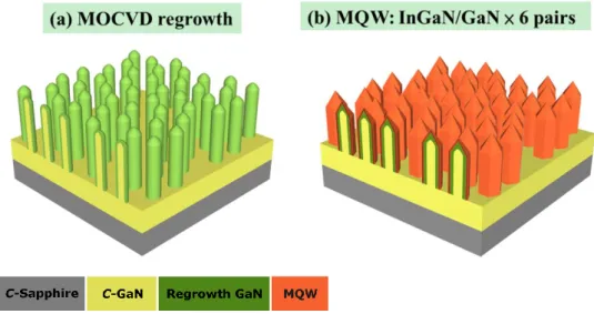
3.1 Procedures of 3-D Core-shell InGaN/GaN Multi-Facet Qunatum Wells Structure on Semipolar { - } and Nonpolar { - } Plane ... 44
3.1.1 Growth Procedure of Nanorods on C-plane (0001) GaN Epilayer Template by
Nano-Imprint Lithography ... 44 3.1.2 Regrowth of Core-Shell Semipolar {10-11} Plane and nonpolar {10-10} Plane
InGaN/GaN MQWs on GaN Nanorods ... 45
3.2 Procedures of 3-D Core-shell InGaN/GaN Multi-Facet Qunatum Wells LED Devices on Semipolar { - } and Nonpolar { - } Plane ... 49
3.2.1 Fabrication of Nanorods and SiO2 Sidewall Passivation ... 49 3.2.2 Device Fabrication of Core-Shell InGaN/GaN MQWs LED Devices on Semipolar {10-11} and nonpolar {10-10} Plane ... 51
3.3 Summary ... 51
3.4 Reference ... 53
CHAPTER 4 GROWTH MECHANISM OF 3-D CORE-SHELL INGAN/GAN
X
AND NONPOLAR { - } PLANE ... 64
4.1 Crystalline Quality and Indium Distribution of 3-D Core-shell InGaN/GaN Multi-Facet Qunatum Wells on Semipolar { - } and Nonpolar { - } Plane ... 65
4.2 Spatial Cathodoluminescence Emission of 3-D Core-shell InGaN/GaN Multi-Facet Qunatum Wells on Semipolar { - } and Nonpolar { - } Plane ... 69
4.3 Summary ... 71
4.4 References ... 73
CHAPTER 5 OPTICAL PROPERTIES OF 3-D CORE-SHELL INGAN/GAN MULTI-FACET QUNATUM WELLS ON SEMIPOLAR { - } AND NONPOLAR { - } PLANE ... 82
5.1 Properties of Spatial Luminescence and Internal Electric Field ... 84
5.2 Tunable Color Temperature of White Light Emission by Nano-facets InGaN/GaN MQWs ... 89
5.3 Photoluminescence of 3-D Core-shell InGaN/GaN Multi-Facet Qunatum Wells on Semipolar { - } Plane and Nonpolar { - } Plane ... 92
5.4 Lasing Action in Gallium Nitride Photonic Quasicrystal Nanorods Arrays ... 101
5.5 Summary ... 106
5.6 References ... 108
XI
CORE-SHELL INGAN/GAN MULTI-FACET QUNATUM WELLS
OPTOELECTRONIC DEVICES ON SEMIPOLAR { - } AND
NONPOLAR { - } PLANE ... 126
6.1 The Light Extraction Efficiency Enhancement of 3-D Core-shell InGaN/GaN Multi-Facet Qunatum Wells on Semipolar { - } and Nonpolar { - } Plane ... 128
6.2 Electrical Properties of 3-D Core-shell InGaN/GaN Multi-Facet Qunatum Wells LEDson Semipolar { - } and Nonpolar { - } Plane ... 133
6.3 Summary ... 139
6.4 References ... 140
CHAPTER 7 CONCLUSION ... 150
PUBLICATION LIST ... 154
XII
Table Captions
Table 1-1. The efficiency of 12 mil standard red, green and Blue LED at injected current 20 mA with carrier density about 2×1017 cm-3. ... 10 Table 2-1. Three types of NIL Eitre® functions. ... 34 Table 4-1. The indium content distribution of point A-F for sample HT and sample LT. ... 76 Table 5-1. The integration of sample HT with the indium content, the thickness of wells and barriers,
the IEF (F0), and the multiple peaks fitting wavelength from the PL spectrum. ... 112
Table 5-2. CIE 1931 Colorimetric Epicenters xe, ye and Constants for Equation 5.20. ... 113
Table 5-3. The x, y, z, n and CCT of sample HT and sample LT were obtained from Equation 5.17-5.21. ... 114 Table 5-4. IQE, activation energy and binding energy for HT- sample. ... 114 Table 5-5. IQE, activation energy and binding energy for LT-sample. ... 114
XIII
Figure Captions
Figure 1-1. External quantum efficiency as a fuction of peak wavelength with two different materials
of InGaN/GaN and AlGaNInP MQWs [1]. ... 10
Figure 1-2. The quantume well structures of InGaN/GaN on (a) polar c-axis and (b) nonpolar orientations and theie band diagrams [2]. ... 11
Figure 1-3. Polarization (spontaneous and piezoelctric) effect as a function of tilt angle of the growth plane with respect to polar [0001] direction [2]. ... 11
Figure 1-4. Schematic illustration of GaN hexagonal crystal structure which indicate the polar {0001} surfaces, the nonpolar {11-20} and {1-100} surfaces, and the semipolar {10-13}, {10-12}, and {11-22} surfaces [2]. ... 12
Figure 2-1. Description of subsystems in a MOCVD apparatus... 34
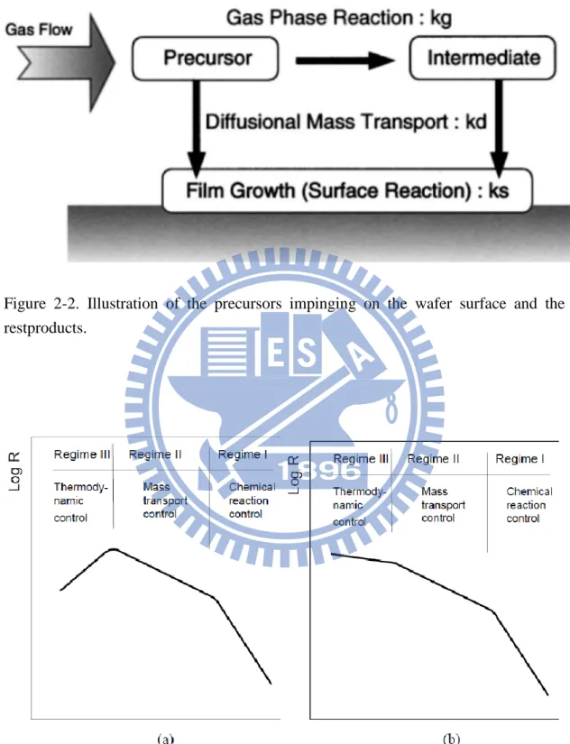
Figure 2-2. Illustration of the precursors impinging on the wafer surface and the restproducts. ... 35
Figure 2-3. Temperature dependence of the deposition rate: (a) exothermic reaction ... 35
Figure 2-4. NIL Eitre® 6 on National Nano Device Laboratories. ... 36
Figure 2-5. Fundamental physical operating mechanism of HDP-RIE. ... 36
Figure 2-6. Schematic of inductive coupling plasma source. ... 37
Figure 2-7. Schematic of SEM instrument. ... 37
Figure 2-8. Schematic illustration of the origin of two sources of secondary electron generation in the sample. ... 38
Figure 2-9. Schematic illustration of the indirect collection of backscattered electrons by a positively biased E-T detector. ... 38
Figure 2-10. Through-the-lens (TTL) detector for SE used in high-performance field emission SEMs. 39 Figure 2-11. Typical experimental set-up for PL measurements. ... 39
XIV
Figure 2-13. Schematic of the luminescence transitions between the conduction band (EC), valence
band (EV), excition (EE), donor (ED), and acceptor (EA) levels in a luminescent material. ... 40
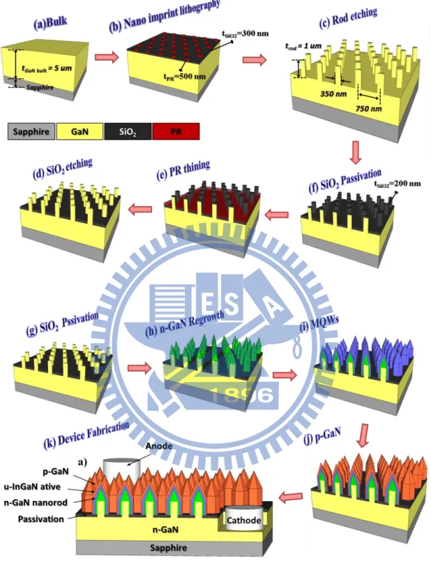
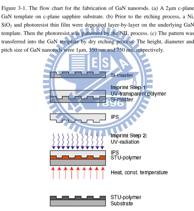
Figure 2-14. The schematic setup of TRPL system. ... 41 Figure 2-15. EL system includes all components. ... 41 Figure 3-1. The flow chart for the fabrication of GaN nanorods. (a) A 2μm c-plane GaN template on
c-plane sapphire substrate. (b) Prior to the etching process, a Ni, SiO2 and photoresist thin
film were deposited layer-by-layer on the underlying GaN template. Then the photoresist was patterned by the NIL process. (c) The pattern was transferred into the GaN template by dry etching process. The height, diameter and pitch size of GaN nanorods were 1μm, 350 nm and 750 nm, respectively. ... 55 Figure 3-2. IPS-STU® technology of nano-imprint lithography, including Intermediate Polymer Stamp
(IPS®) and Simultaneous Thermal and UV (STU®). ... 55 Figure 3-3. The schematic illustration of the regrowth process: (a) The deposition of n-GaN and the
pre-strain layer on GaN nanorods. (b) Six pairs of InGaN/GaN MQWs conformally grew on GaN nanorods. ... 56 Figure 3-4. The SEM images viewed in 45∘of (a) GaN nanorods, (b) the regrowth InGaN/GaN MQWs
on GaN nanorods of sample HT and (c) sample LT, respectively. (d) The schematic
representation of the regrowth process for core-shell nanorods. ... 56 Figure 3-5. (a) Plane view SEM image of the fabricated nanorod arrays. (b) and (c) A 12-fold photonic
quasicrystal pattern [3]. (d) The average radius and the pitch of nanorods are about 175nm and 750nm, respectively. ... 57 Figure 3-6. (a) The procedure illustration of defect reduced via NIL technology. (b) Cross-section
STEM micrograph of sample HT. The red cicle indicate a TD which is buried in the underlying template... 58 Figure 3-7. Cross-sectional STEM micrograph of core-shell nanorods with TDs were bended to
XV
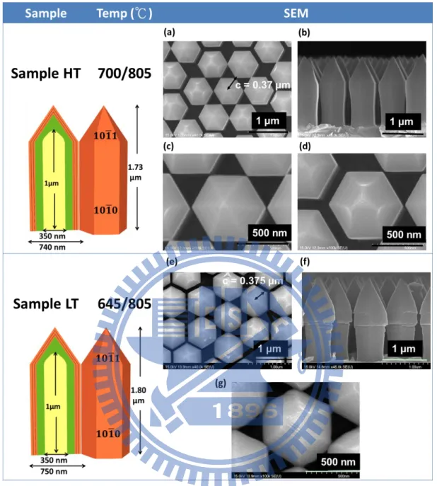
side-wall surfaces and penetrate to the shell of MQWs, indicating by the red circle... 58 Figure 3-8. (a), (c), (d) and (b) are top-view and cross-section SEM images of sample HT, respectively.
(e), (g) and (f) are top-view and cross-section SEM images of sample LT, respectively. ... 59 Figure 3-9. The evolution of sidewall passivation fabrication. ... 60 Figure 3-10. (a) side wall passivation using SOG and (b) PECVD. ... 61 Figure 3-11. (a) the fitting curve of the etching rate of PMMA in O2 plasma; (b) cross section view of
the nanorod template after PMMA coating; (c) bird's-eye view and (d) cross section view of 100s O2 plasma etching; (e) bird's-eye view and (f) cross section view of 200s O2 plasma
etching. ... 62 Figure 3-12. The fabrication flowchart of core-shell semipolar and nonpolar InGaN/GaN LEDs. ... 63 FFigure 4-1. (a) A top-view SEM image of a GaN nanorod for sample HT. (b) A TEM micrograph of a
core-shell nanorod view in the zone axis. (c) Electron diffraction pattern confirmed core-shell nanorods with single-cyrstal nature of zone axis. (d) The different crystalline orientation nano-facets on core-shell nanorods. B-F, the indium content distribution and the growth rate of InGaN/GaN wells and barriers versus distance with the normal direction at each point from the first to sixth pairs of MQWs. ... 77 Figure 4-2. (a) A top-view SEM image of a GaN nanorod for sample LT. (b) A TEM micrograph of a
core-shell nanorod view in the zone axis. (c) Electron diffraction pattern confirmed core-shell nanorods with single-cyrstal nature of zone axis. (d) Red circles show the indium clusters on nonpolar planes. A-D and F, the indium content distribution and the growth rate of InGaN/GaN wells and barriers versus distance with the normal direction at each point from the first to sixth pairs of MQWs. ... 78 Figure 4-3. (a) SEM top-view image of sample HT. (b) Spatially integrated CL spectrum of (a). (c)-(i)
Spectrally resolved CL images showing the location dependent emission wavelength of quantum wells. ... 79
XVI
Figure 4-4. (a) SEM cross-section image of sample HT. (b) Spatially integrated CL spectrum of (a). (c)-(i) Spectrally resolved CL images showing the location dependent emission wavelength of
quantusm wells. ... 80
Figure 4-5. (a) TEM cross section view of a nanopillar, showing the growth of six QWs (dark colored lines), the InN fraction, and well/barrier thickness.(b) Close view at the pyramid facet and pillar sidewall junction. ... 81
Figure 4-6. (a) SEM top view of nanopillars showing two different pyramid geometries (labeled as H and T). (b) Close view of the pyramid T. (c) Schematic showing the facet evolution of pyramid T, transforming from hexagonal to triangular pyramid facets from bottom to top. ... 81
Figure 5-1. The PL spectra as a function of the excitation power for (a) sample HT and (d) sample LT. Multiple peaks fitting of MQWs emission ranging from blue to green with the ensemble PL spectrum of (b) sample HT and (e) sample LT. The emission wavelength as the function of the pumping power of (c) sample HT and (f) sample LT. ... 116
Figure 5-2. (a) Computed wavelength of sample HT by APSYS. (b) The corresponding position and wavelength of the spatially resolved CL image. (c) Multiple peaks fitting of MQWs emission from the ensemble PL spectrum of the excitation power at 10 mW... 116
Figure 5-3. (a) The emission wavelength as the function of the pumping power of sample HT. The PL peak emission energy as the function of the excitation power for with different excitation power for (b) semipolar planes and (c)-(d) nonpolar planes at room temperature. The dots are the experimental value from the PL measurement at room temperature, whereas the solid lines are the fitting results for the IEF. (e) The IEF corresponds to the position of core-shell nanorod. ... 117
Figure 5-4. The idealized equivalent circuit of p-n junction under illumination [3]. ... 118
Figure 5-5. Color matching functions were established by CIE in 1931. ... 119
XVII
Figure 5-7. Red circle and blue square represent HT and LT sample on CIE 1931 chromaticity diagram, respectively.. ... 120 Figure 5-8. Schematic of effective localized states, defect states and activation energy. ... 121 Figure 5-9. Activation energy fitting for (a) HT-sample and (b) LT-sample. ... 121 Figure 5-10. Emission energy versus temperature and the fitting of Varshni’s equation for HT-sample. ... 122 Figure 5-11. Illustration of radiative and nonradiative transition in a semiconductor. ... 122 Figure 5-12. TRPL measurement of the nonpolar (10-10) blue emission at (a) 15 K, (b) 300K and the
semipolar (10-11) green emission at (c) 15 K, (d) 300K. ... 123 Figure 5-13. 𝝉𝑷𝑳, 𝝉𝒓 and 𝝉𝒏𝒓 versus temperature of (a) the nonpolar (10-10) blue emission and
(b) the semipolar (10-11) green emission ... 123 Figure 5-14. Radiative lifetime (𝝉𝒓) and the fitting curve for dimensional of excition of both nonpolar (10-10) blue emission and semipolar (10-11) green emission. ... 124 Figure 5-15. (a) Integrated emission power versus pump intensity, showing the onset of lasing action.
Inset graph shows the emission spectrum versus pump intensity. (b) Threshold pump intensity versus pump spot area and the power law fitting curve showing a threshold pump intensity Pth ~ 1/A0.27 dependence. ... 124
Figure 5-16. (a) The quasicrystal model used in FDTD simulation. (b)-(d) The resonant spectra obtained by launching broad band pulses at locations labeled correspondingly in Figure 5-16 (a)... 125 Figure 5-17. (a)-(c) Mode field patterns correspond to the resonant peaks labeled as 6(a), 6(b), and
6(c) in Figure 5-16. ... 125 Figure 6-1. Illustration of various potential white-light LEDs configurations [9]. ... 143 Figure 6-2. Light traveling within waveguides (left) with a smooth interface and (right) with a rough
XVIII
Figure 6-3. Simulation step of FDTD method. ... 144 Figure 6-4. FDTD calculus from near field transfer to far field. ... 144 Figure 6-5. (a)-(e) are our diagram of simulation structure. ... 144 Figure 6-6. (a) The output intensity various wavelength; (b) The enhancement of PSS, p-side rough,
pyramid-like rough and pyramid. ... 145 Figure 6-7.The distribution of far-field angle for each structures ... 145 Figure 6-8. The SEM image of SiO2 sidewall passivation ... 146
Figure 6-9. The emmision color of core-shell LED on CIE 1931 chromaticity diagram dependant on driving current of 5, 10, 20, 40, 80, 160 mA. ... 146 Figure 6-10. (a) LIV Curve and (b) EL spectrum of the core-shell LED. ... 147 Figure 6-11. Light emission photographs of core-shell LED at a forward current of (a) 5mA, (b) 10mA,
(c) 20mA, (d) 40mA, (e) 80mA, and (f) 160mA. ... 147 Figure 6-12. Light emission photographs of core-shell LED at a forward current of (a) 2.2 V, (b) 2.4 V,
(c) 2.6 V, (d) 2.8 V, (e) 3.0 V, (f) 3.2 V, (g) 3.4 V, and (h) 3.6 V. ... 148 Figure 6-13. (a) LIV Curve and (b) EL spectrum of Ref-LED. ... 148 Figure 6-14. The optical microscope of polar blue LED at a forward current of (a) 5mA, (b) 10mA, (c)
20mA, (d) 40mA, (e) 80mA, (f) 160mA. ... 149 Figure 6-15. (a) The simulation region and structure; The geometric electrical field when applied
Chapter 1
Introduction
1.1 Specific Properties of Gallium-Nitride (GaN) Based
Devices
The III-nitrides are a remarkable material system. With direct bandgap (Eg), III-nitrides are spanning from the deep ultraviolet (InN, Eg = 0.7 eV) through the ultraviolet (GaN, Eg = 3.4 eV) and visible to infrared (AlN, Eg = 6.0 eV) range. There have been great research interests in GaN material due to its promising applications in UV to blue optoelectronic devices and strong emission properties.
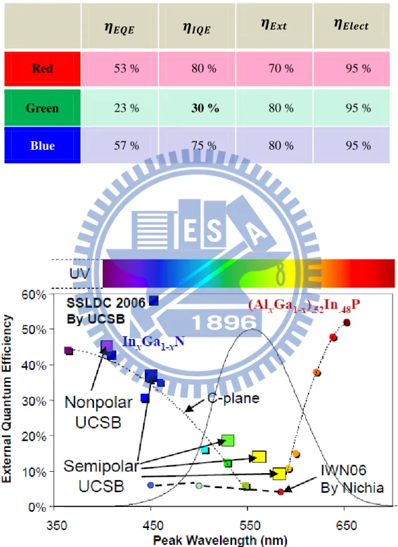
GaN based light-emitting diodes (LEDs) were applying for many aspects in daily life, e.g., traffic lights, indoor lighting, liquid crystal display (LCD) backlighting, architecture illumination, etc. For global energy savings, LEDs was a new light source, but LEDs also had their own drawbacks and challenges, as stated in the following: the external quantum efficiency as a function of emission wavelengths in the visible range for LEDs was shown in Figure 1-1. Above 450 nm, UV and blue LEDs had the external quantum efficiency about 30-40%, but around 525 nm green LEDs only reach 10-20%, mainly due to quantum confined Stark effect (QCSE) became stronger at longer wavelengths, this is so-called green gap. The same as AlGaInP for red LEDs also became very dim in the green emission [1]. There are many factors have effect on EQE from fabrication flow chart of LED:
where ηEQE is the EQE, ηIQE is the internal quantum efficiency (IQE), ηExt is the
light extraction efficiency, ηElect is the electrical loss.
Table 1-1 shows the standard red, green and blue LEDs efficiency of 12 mil chip
size at injected current 20 mA with carrier density about 2×1017 cm-3. If the IQE of green LED could be improved the realization of full collar LED is very promising. Conventional LEDs and LDs were usually grown on polar c-plane GaN, and the strained quantum well structures were grown along the polar direction. However, its related devices have a significant problem with strong built-in electric fields caused by both spontaneous and piezoelectric polarization, bending the energy bands of the InGaN active region, as shown in Figure 1-2 (a). These electric fields lead to a spatial separation of the electron and hole wavefunctions, it is the well-known QCSE. QCSE results in a reduced radiative recombination rate to lower the internal quantum efficiency and causes a large blue shift in the electroluminescence with increasing drive current. It is expected that nonpolar planes would eliminate QCSE, as shown in
Figure 1-2 (b). The strain-induced polarization can be avoid by the employment of
nonpolar planes, when the growth direction perpendicular to the polar c-axis. As the computed polarization charge, semipolar planes also have the similar effects for nonpolar planes to mitigate QCSE [2], as shown in Figure 1-3.
Crystal structure of GaN is most stable as the hexagonal wurtzite (WZ) type in space group P63mc. There are three low index faces compose in the hexagonal
structure, including polar ( ) +c-plane (Ga-face), ( ̅) –c-plane (N-face), nonpolar ( 2̅ ) a-planes and ( ̅ ) m-planes. The high index facets such as semipolar ( ̅3), ( ̅ ) and ( 2̅2) planes are inclined to the [0001] polar direction, as shown in Figure 1-4.
On the other hand, the lighting efficiency decreases in long emission InGaN/GaN multi-quantum wells (MQWs) with increasing indium content. There are mainly three mechanisms to cause the strain relaxation including phase separation, plastic relaxation and elastic relaxation. The spinodal decomposition mainly caused by the thermodynamic properties of InGaN alloy. The large interatomic spacing difference (11%) between InN and GaN results in phase separation [3]. In addition, a high indium content of InGaN films requires fairly low growth temperatures also owing to the thermodynamic properties. At quite low growth temperature, InGaN films grow with high indium content but poor crystalline quality [4]. Moreover, InGaN thin film had pseudomorphic growth on the underlying GaN template. The deleterious dislocations lead to plastic strain relaxation when InGaN films exceed its critical thickness. The InGaN/GaN MQWs grown on three dimensional structures induce the elastic relaxation by Stransky-Krastanov transition [5]. The problem of low indium incorporation efficiency is exist in all crystllographic orientation of WZ stucture. However, several groups proposed semipolar planes such as ( ̅3), ( ̅ ) and ( 2̅2) with comparable high indium incorporation efficiency and little polarization effects than that observed in c-plane GaN [6-8].
1.2 Perspectives of GaN Based Polychromatic Nano-emitters
Conventionally devices are built in two-dimensional c-plane GaN structures but have the large QCSE. Several groups had proposed many methods to solve the QCSE in polar c-plane, such as thinner QW thickness [9], composition-graded barrier [10], pre-strain layer [11] and p-InGaN barrier [12], but the results were limited. Semipolar or nonpolar GaN substrate also had been proposed to avoid the polar orientation [8], but the cost was too high. In recent years, devices with one-dimensional nanostructure have gained substantial attention for their interesting properties and potential applications [13, 14]. The one-dimensional structures can be fabricated by top-down patterned etching like photolithography or bottom-up self-assembled growth processes such as the vapor-liquid-solid (VLS) growth mechanism [15].
The polychromatic emission of nano-emitters had been investigated by many groups. By using molecular beam epitaxy (MBE), different emission color control from blue to red with nanocolumn diameter from 143 nm to 270 nm of InGaN/GaN nanocolumn arrays [16]. Recent work to generate a phosphor-free natural white light emission (6000K) was using self-assembled GaN nanorods array with thick InGaN nanodisks to fabricate full-color InGaN nanodisk emitters [17]. By using metal organic chemical vapor deposition (MOCVD), Funato et. al. proposed phosphor-free monolithic polychromatic LEDs with different emission wavelength mainly owing to the different incorporation efficiency on the multi-crystalline micro-facets. Therefore, the fabrication of monoclinic full-color nano-emitters is expected to replace the blue LEDs with yellow phosphor to generate white light emission.
1.3 Motivation
In recent years, significant interest has developed in the potential of using one dimensional GaN nano structures as an alternative design to improve the efficiency of the commonly-used planar structure GaN light emitting diodes. The nanopillar structure provides several advantages over the planar structure. The nanopillar exhibits a significantly reduced defect density because it has only a small area of contact with the growth template. This small footprint reduces strain from the lattice and thermal expansion coefficient mismatch between the GaN nanopillar and the growth template [19-21], thus reducing piezoelectric polarization and improving electron-hole recombination efficiency [22, 23]. The reduced strain also allows for higher In concentration in InGaN/GaN MQWs for green-red color emission applications [16, 17, 24]. These advantages have been demonstrated in MQWs grown in the nanopillar axial direction, which is often the c-axis crystal direction. The nanopillar offers an additional option to grow MQWs on the pillar surfaces in a core-shell geometry. These surfaces can be nonpolar or semipolar crystal planes with zero or low polarization fields. The MQWs grown on these planes have a lower carrier density dependent wavelength change and a higher radiative recombination efficiency [25-27]. This structure can also result in a much larger active surface area than found in MQWs grown on the nanopillar axial direction. Due to the nature of their three dimensional structure, the growth and emission properties of core-shell MQWs can vary with different crystal planes and require investigation.
GaN nanopillars can be fabricated by either a bottom-up or top-down approach. The former grows vertical nanopillars upward from a substrate by molecular beam epitaxy or hydride vapor phase Epitaxy [16-18, 24]. The nanopillars are often formed
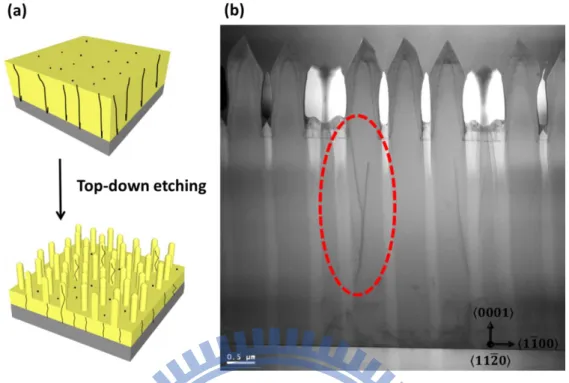
by self-assembly. This approach provides less control over the size and location of nanopillars. The latter approach creates nanopillars by etching a flat substrate downward with circular etching masks [28], providing improved dimension and pattern control. The etching process usually produces damaged surfaces that may require repairs. Here, we report a fabrication process using top-down patterned etching followed by an epitaxial regrowth to create crystalline core-shell MQW nanopillar arrays.
As described in the above sections, the difficulties in growing devices on c-plane GaN with long wavelength emission is due to the QCSE along [0001] polar-direction. The employment of nonpolar or semipolar planes which are inclined or perpendicular to polar c-planes can eliminate or mitigate the QCSE. The indium phase separation of InGaN alloy exists in all crystalline direction of WZ structure; however, the indium incorporation efficiencies are different from different orientations. It is expected that a monolithic light emission can be fabricated by phosphore-free nano-emitters. In order to fabricate high lighting efficiency nano-emitter, we use one-dimensional core-shell nanorod structure which has the following advantages: the reduction of dislocations, the promotion of light extraction efficiency and the enlarged active area.
The lighting efficiency of LEDs is determined by the product of the internal quantum efficiency and the light extraction efficiency. The internal quantum efficiency is defined as the ratio of the number of injected electrons to that of electron-hole pairs which emitted from active area. The light extraction efficiency is defined as the ratio of the number of generated photons to the number of photons extracted from the devices.
semipolar and { ̅ } nonpolar planes under the MOCVD growth process. At the same time, the geometric structure in three-dimension of core-shell nanorods also enlarge the active area which is compared to the planar structures. Therefore, the two factors for the promotion of internal quantum efficiency are predictable.
In comparison to planar thin film devices, GaN-based LEDs with photonic quasicrystal (PQC) structures are attracting much interest [17]. The motivation for using a PQC structure is to promote the light extraction efficiency in optical devices. For the large refractive index difference of GaN-based semiconductor (n=2.5) and air (n=1), most of the light rays emitting from the planar active region are total internally reflected at semiconductor’s surface. Therefore, enhancement of the light extraction efficiency is especially important. The critical anlge (𝜃𝑐=23.6。) for total internal
reflection is obtained by using snell’s law
𝑛̅𝑎𝑖𝑟sin 9 ° = 𝑛̅𝐺𝑎𝑁sin 𝜃𝑐 (1.2.)
In this thesis, there is an open window for growing high efficiency optical devices with monolithic polychromatic emission by using core-shell InGaN/GaN MQWs grown on GaN nanorod. The experimental results, the specific properties of core-shell nanorods and the brief conclusions and future works are available in the following chapters.
1.4 References
[1] S. Nakamura, "Current status of GaN-based solid-state lighting," MRS bulletin, vol. 34, pp. 101-107, 2009.
[2] H. Masui, et al., "Nonpolar and Semipolar III-Nitride Light-Emitting Diodes: Achievements and Challenges," Electron Devices, IEEE Transactions on, vol. 57, pp. 88-100, 2010.
[3] S. Keller, et al., "Growth of bulk InGaN films and quantum wells by atmospheric pressure metalorganic chemical vapour deposition," Journal of crystal growth, vol. 170, pp. 349-352, 1997.
[4] J. Speck and S. Rosner, "The role of threading dislocations in the physical properties of GaN and its alloys," Physica B: Condensed Matter, vol. 273, pp. 24-32, 1999.
[5] M. Leyer, et al., "The critical thickness of InGaN on (0001) GaN," Journal of
crystal growth, vol. 310, pp. 4913-4915, 2008.
[6] N. Okada, et al., "Growth of Semipolar (11-22) GaN Layer by Controlling Anisotropic Growth Rates in r-Plane Patterned Sapphire Substrate," Applied
physics express, vol. 2, pp. 091001-1, 2009.
[7] R. Sharma, et al., "Demonstration of a semipolar (1013) InGaN/GaN green light emitting diode," Applied Physics Letters, vol. 87, pp. 231110-231110-3, 2005. [8] B. Gil, "Symmetry properties and anisotropic excitonic response for GaN films
grown on semipolar (11-22)-, (10-11)- and (10-13)-oriented GaN substrates,"
Applied Physics Letters, vol. 90, pp. 121903-121903-3, 2007.
[9] J. Bai, et al., "Influence of the quantum-well thickness on the radiative recombination of InGaN/GaN quantum well structures," Journal of Applied
Physics, vol. 88, p. 4729, 2000.
[10] T. Onuma, et al., "Improved Emission Efficiency in InGaN/GaN Quantum Wells with Compositionally-Graded Barriers Studied by Time-Resolved Photoluminescence Spectroscopy," Japanese Journal of Applied Physics Letters, vol. 42, pp. 1369-1371, 2003.
[11] C. Huang, et al., "Enhanced efficiency and reduced spectral shift of green light-emitting-diode epitaxial structure with prestrained growth," Journal of
Applied Physics, vol. 104, pp. 123106-123106-7, 2008.
[12] J. Ryou, et al., "Control of quantum-confined Stark effect in InGaN¢A GaN multiple quantum well active region by p-type layer for III-nitride-based visible light emitting diodes," Applied Physics Letters, vol. 92, p. 101113, 2008.
nanophotonics," Nano Letters, vol. 4, pp. 1975-1979, 2004.
[14] L. Gangloff, et al., "Self-aligned, gated arrays of individual nanotube and nanowire emitters," Nano Letters, vol. 4, pp. 1575-1579, 2004.
[15] R. Yan, et al., "Nanowire photonics," Nature photonics, vol. 3, pp. 569-576, 2009.
[16] H. Sekiguchi, et al., "Emission color control from blue to red with nanocolumn diameter of InGaN/GaN nanocolumn arrays grown on same substrate," Applied
Physics Letters, vol. 96, pp. 231104, 2010.
[17] H. Lin, et al., "InGaN/GaN nanorod array white light-emitting diode," Applied
Physics Letters, vol. 97, pp. 073101, 2010.
[18] Z. Zhang, et al., "Effects of symmetry of GaN-based two-dimensional photonic crystal with quasicrystal lattices on enhancement of surface light extraction, "
Applied Physics Letters, vol. 88, p. 171103, 2006.
[19] J. Chang, et al., “Strong luminescence from strain relaxed InGaN/GaN nanotips for highly efficient light emitters, ” Opt. Express, vol. 15, p. 9357, 2007.
[20] J. Renard, et al., “Evidence for quantum-confined Stark effect in GaN/AlN quantum dots in nanowires, ” Phys. Rev. B, vol. 80, p. 121305, 2009.
[21] Q. Li and G. Wang, “Strain influenced indium composition distribution in GaN/InGaN core-shell nanowires,” Appl. Phys. Lett., vol. 97, p. 181107, 2010. [22] Y. Chang, et al., “High efficiency green, yellow, and amber emission from
InGaN/GaN dot-in-a-wire heterostructures on Si(111),” Appl. Phys. Lett., vol. 96, p. 013106, 2010.
[23] Y. Hong, et al., “Visible-Color-Tunable Light-Emitting Diodes,” Adv. Mater., vol.
23, p. 3284, 2011.
[24] H. Nguyen, et al., “Controlling Electron Overflow in Phosphor-Free InGaN/GaN Nanowire White Light-Emitting Diodes,” Nano Lett., vol. 12, p. 1317, 2012. [25] R. Koester, et al., “M-Plane Core–Shell InGaN/GaN Multiple-Quantum-Wells on
GaN Wires for Electroluminescent Devices,” Nano Lett., vol. 11, p. 4839, 2011. [26] C. Lee, et al., “GaN/In −xGaxN/GaN/ZnO nanoarchitecture light emitting diode
microarrays,” Appl. Phys. Lett., vol. 94, p. 213101, 2009.
[27] T. Yeh, et al., “Vertical nonpolar growth templates for light emitting diodes formed with GaN nanosheets,” Appl. Phys. Lett., vol. 100, p. 033119, 2012. [28] Q. Li, et al., “ptical performance of top-down fabricated InGaN/GaN nanorod
Table 1-1. The efficiency of 12 mil standard red, green and Blue LED at injected current 20 mA with carrier density about 2×1017 cm-3.
𝜼
𝑬𝑸𝑬𝜼
𝑰𝑸𝑬𝜼
𝑬𝒙𝒕𝜼
𝑬𝒍𝒆𝒄𝒕Red 53 % 80 % 70 % 95 %
Green 23 % 30 % 80 % 95 %
Blue 57 % 75 % 80 % 95 %
Figure 1-1. External quantum efficiency as a fuction of peak wavelength with two different materials of InGaN/GaN and AlGaNInP MQWs [1].
Figure 1-2. The quantume well structures of InGaN/GaN on (a) polar c-axis and (b) nonpolar orientations and theie band diagrams [2].
Figure 1-3. Polarization (spontaneous and piezoelctric) effect as a function of tilt angle of the growth plane with respect to polar [0001] direction [2].
Figure 1-4. Schematic illustration of GaN hexagonal crystal structure which indicate the polar {0001} surfaces, the nonpolar {11-20} and {1-100} surfaces, and the semipolar {10-13}, {10-12}, and {11-22} surfaces [2].
Chapter 2
Experimental Apparatus
2.1 Metalorganic Chemical Vapor Deposition (MOCVD)
Metalorganic Chemical Vapor Deposition (MOCVD) is the most common epitaxial technique used in both industry and research. It has the benefit of high growth rate on large area wafers. One problem with MOCVD is that it requires complicated and sometimes vary hazardous gases in order to produce the epitaxial layer. Compound semiconductors are grown from the surface reaction of organic compounds or metalorganics and hydrides containing the required species. In growing GaN hydride mixture containing ammonia and trimethyl-gallium (TMGa), highly diluted by hydrogen or nitrogen, is led into the reactor separately. Figure 2-1 shows a schematic drawing of the MOCVD subsystem. The vapor pressure of the MO source is a function of temperature. By placing the MO bottle in a bath containing a mixture of water and glycol, the vapor pressure can be controlled over a wide range of temperature. The carrier gas is “bubbled” through the MO liquid and transport into the line. The amount of vapor transported into the line depends on the flow rate of the carrier gas (Φc), the pressure in the bottle (Pb) and the vapor pressure Pvap of the MO
(ΦMO). When growing epitaxial films in the reactor, it is of great importance to know
how much source material is introduced. Since the volume and the temperature of the source bottle is constant, the perfect gas law can be used to determine the flow rate of MO (ΦMO). During a time interval Δt, ΦMO.Δt α n moles of source material is
(2.1)
where Pc is the partial pressure of the carrier gas in the bottle. In the gas panel
configuration shown in Figure 2-1, the pressure in the bottle is controlled from the following line. The partial pressure of the source gas can be expressed as Pc= Pb-
Pvap. Inserting into Equation 2.1 the flow rate of the MO (in cm3/min) can be
evaluated.
The precursor molecules NH3 and TMGa are fed in separately into the
reactorchamber. In the reactor reactions take place both on the wafer and before the molecules reach the wafer. Formation of the epitaxial layer occurs by the reaction:
Ga(CH3)3 + NH3 → GaN + CH4 (2.2)
Figure 2-2 illustrates the growth process with impinging precursors and rest
products. Due to the low cracking efficiency of ammonia and adatom mobility the growth of GaN is carried out at very high temperature around 1000°C ~1100°C to high crystalline quality. Many of the difficulties involving the growth of GaN are due to the high volatility of nitrogen. The pressure of nitrogen in the vapor must not be below a certain value to produce the solid without other phases. If the pressure is too low, a Ga liquid phase is formed resulting in droplet formation on the surface of crystal (GaN + 3/2H2 → Ga + NH3). An alternative precursor to NH3 for atomic
nitrogen is dimethyl-hydrazine [1]. It has successively been used for growth of GaN
[2]. Dimethyl-hydrazine has a relatively low decomposition temperature compared to NH3. At 420°C it decompose up to 50% [3], while NH3 only 15% at 950°C.
the region II in Figure 2.3. This regime appears at moderate temperatures. Compared with the chemical reaction regime the mass transport rate of the reactant gaseous species is much lower than that of the chemical reaction, i.e. hG << kS. The coating
growth is limited by the mass transport from the bulk gas to the substrate surface. In this case a steep concentration gradient within the boundary layer is generated and the reactant gaseous species are nearly consumed on the substrate surface.
In this regime, the temperature dependence of the growth rate becomes mild, which is attributed to the gaseous species diffusivity. The growth rate of the coating increases linearly with the partial pressure increasing of the reactant gaseous species (preact), which is confirmed through experimental work as shown in Figure 2.3. The
growth rate is inversely proportional to the total pressure in the system. The mass transport rate can be considerably enhanced through a decrease in the total pressure. This is the main reason that most CVD processes are operated at reduced pressures. An increase in the gas velocity in the bulk is useful to reduce the thickness of the boundary layer and, hence, results in a more rapid growth rate of coatings.
For the growth of monolithic materials the high growth rate is much more important than the thickness uniformity from an economical view. The MOCVD processes are often performed in the mass transport regime. The higher processing temperatures are used for thermal gradient CVI and forced CVI processes in which fast growth rates are needed to ensure the rapid densification of the composites.
2.2 Nano-Imprint Lithography Equipment
Nanoimprint lithography (NIL) is a novel technology which can achieve flexible dimension range on semiconductor devices. The first publication in 1995 was from Chou et al. on thermal NIL. After that, many NIL methods, including thermal nano imprint lithography (NIL), UV NIL and Obducat's proprietary Simultanous Thermal and UV (STU® ) imprint process, are developing quickly on past few years. It becomes a significant technology for scientists studying. Helmut Schift defined: NIL
as a parallel patterning method in which a surface pattern of a stamp is replicated into a material coated on a hard substrate by mechanical contact and 3D material displacement, to be used in fields until now reserved to electron beam lithography (EBL) and photolithography (PL). Nanoimprint lithography (NIL) is a next generation
lithography (NGL) candidate technology.
One of the serious issues is contamination the stamp after imprinting process. Obducat’s nanoimprint lithography (NIL) technology has solved it by using the Intermediate Polymer Stamp (IPS®). Obducat is the world-leading naoimprint lithography equipment supplier. The Eitre® Nano Imprint Lithography (NIL) series, including Eitre® 3, 6, and 8, is the studying and development machines which offer a flexible and efficient lithography solution. Table 2-1 shows all above have similar functions. There are different on imprinting wafer sizes and suitable for replicating patterns in the micro- and nanometer range. All Obducat nanoimprint lithography (NIL) systems are equipped with standard full area thermal imprint and offers using the patented Soft Press® technology. For example, Figure 2-4 shows the NIL Eitre® 6 facility on National Nano Device Laboratories (NDL). It possesses thermal and UV source to model different patterns. The specific design of the heater which provides a
homogeneous temperature distribution across the whole imprint area is embedded in the substrate chuck and the UV source is embedded on the roof over the substrate chuck. The uniform heating and light source make it possible to use a wide range of imprint polymer.
2.3 Inductively Coupled Plasma Reactive Ion Etching
(ICP-RIE)
It has been demonstrated that conventional RIE is perfectly capable of etching sub-100 nm structures. The only limitation is its relatively low etch rate, which is normally less than 200 nm min–1 for Si. The etching rate in RIE directly depends on plasma density. For the conventional RIE system as shown in Figure 2.5, plasma density increases with increase of RF power. However, increasing RF power will also increase the self-biasing voltage on the cathode where the etching sample is situated. The consequence is the increase of ion bombardment energy, hence deterioration of etching selectivity. This becomes a particularly serious problem in sub-100 nm RIE, because the masking layer is always thin to enable photon or e-beam patterning of polymer resist at sub-100 nm feature dimension.
Inductively coupled plasma (ICP) system has cleverly solved the problem. In an ICP source, the plasma generation is separated from etching chamber, as shown in
Figure 2-6. Radio frequency power is coupled into plasma chamber by an induction
coil from outside. The sample stage is connected to a second RF power source as an auxiliary RF source to enhance the production of plasma. Electromagnetic field generated by inductive coupling coil can sustain electron cycling movement in plasma
for a long period, which has greatly increased ionization probability while keeping the pressure low in the etching chamber. As the sample stage has an independent input of RF power, the self-biasing voltage can be independently controlled. Therefore, an ICP system can produce very high plasma density (>5×1011 cm–3) compared to conventional RIE (108~1010 cm–3), as well as maintain low ion bombardment energy. The conflict between high plasma density and high etch selectivity encountered in conventional RIE systems has been resolved. With such high plasma density and high etching selectivity, high etching rate and deep RIE (DRIE) become possible.
ICP-RIE has been widely used for etching other materials, especially the III-nitride semiconductors. The ICP with high plasma density offers much higher etch rate and selectivity than it is possible by conventional RIE. For example, GaN or sapphire is known to be difficult to etch. With a conventional RIE, the etch rate is less than 5nm min–1. Using an ICP-RIE the etch rate is nearly 10 times enhanced. Inductively coupled plasma systems are widely used to etch III–V semiconductor materials which are of great importance in high frequency and optoelectronic applications currently.
2.4 Electron Microscopy
2.4.1 Scanning Electron Microscopy (SEM)
It is worthwhile to understand the technique and type of instrument of SEM. Very simply; the SEM scans a sample with a beam of electrons that interact with the sample. Some of those electrons and other electrons generated during this process escape from the sample and reach a detector. The number of electrons that reach the
detector at each point on the sample depends on the topology of the sample and the atomic weight of the atoms at the surface, and these variations in signal strength lead to image formation.
A SEM column consists of an electron gun, one or two condenser lenses, an objective aperture, and an objective lens [4]. The electron gun produces a source of electrons and accelerates the electrons to energy of 1~30 keV. This occurs in a vacuum environment ranging from 10-4 to 10-10 Torr. The electron lenses in the column are used to demagnify the image of the gun crossover and focus a final spot on the specimen on the order of nm~ μm with a beam current in the range of pA~ μA. The condenser lens controls the amount of demagnification and the probe forming or objective lens focuses the final probe on the specimen. A schematic of a typical SEM is shown in Figure 2-7.
The lens and aperture system in the column provide control of the beam through manipulation of the probe diameter, probe current, and convergence angle. These three parameters can be controlled and used to achieve high depth-of-field, high-resolution, or high beam current for x-ray microanalysis. A small convergence angle is needed for high depth-of-field imaging and can be obtained with a small objective aperture and a long working distance. High resolution imaging requires a small probe size which can be obtained with a strong condenser lens, an objective aperture, and a short working distance. Finally, x-ray microanalysis may require higher beam currents which can be obtained by weakening the condenser lens and removing the objective aperture.
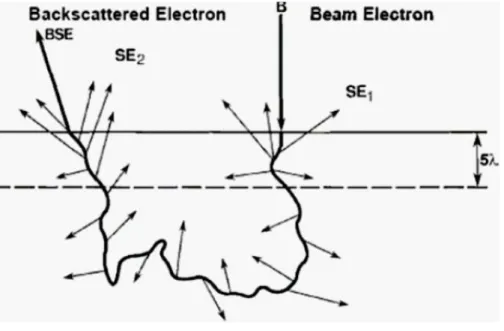
The interactions between the electron beam and the specimen in a SEM are the source for a wide variety of signals that can be collected and used to characterize the
sample as in Figure 2-8. The electron beam-specimen interactions are a result of elastic and inelastic scattering processes that occur simultaneously within the sample. The region in which the electrons interact with the specimen is called the interaction volume. The interaction volume can extend from a few nanometers to a few microns below the surface depending on the beam and sample parameters. Elastic scattering events produce large angular changes in the trajectory of the beam electrons inside the sample, but result in little or no change to the energy of the electron, thus giving rise to the overall shape of the interaction volume. Elastic scattering primarily gives rise to backscattered electrons (BSE). Inelastic scattering events result in the transfer of energy from the beam electrons to the tightly bound inner-shell electrons and loosely bound outer-shell electrons of the atoms in the specimen with very little angular change in the trajectory of the beam electron. During a single inelastic scattering event the beam electron can transfer an amount of energy ranging from less than 1 eV to the full energy carried by the beam electron. Inelastic scattering limits the range of the electrons within the specimen by eventually reducing the electron energy to zero. Inelastic scattering gives rise to phonons (lattice vibrations), plasmons (electron oscillations), auger electrons, characteristic x-rays, continuum x-rays, secondary electrons (SE), and electron hole pair (EHP) generation. EHP generation in a material with a bandgap is the basis for the EBIC and CL signals.
The incident electrons interact with a certain volume of the sample called the interaction volume. There are numerous analytical expressions that have been used to model the size and shape of this interaction volume, which will not be covered here. The interaction volume depends on a number of factors, including the beam energy, the atomic number of the specimen, and the angle the incoming probe beam makes with the sample surface. The number of backscattered and secondary electrons (BSE
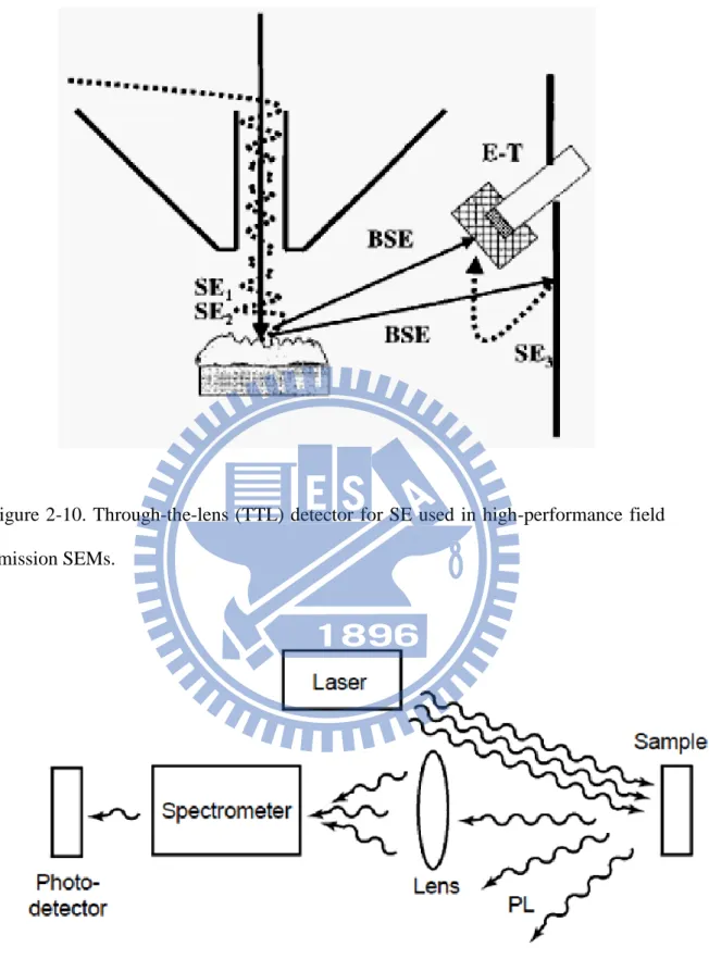
and SE) produced will depend on these parameters and others such as the topology of the sample, and will result in the image contrast observed. Several detection systems are depicted in Figure 2-9 and 2-10.
2.4.2 Transmission Electron Microscopy (TEM)
The transmission electron microscopy (TEM) is used to characterize the microstructure of materials with very high spatial resolution. Information about the morphology, crystal structure and defects, crystal phases and composition, and magnetic microstructure can be obtained by a combination of electro-optical imaging (2.5Å point resolution), electron diffraction, and small probe capabilities. The trade-off for this diverse range of structural information and high resolution is the challenge of producing very thin samples for electron transmission.
The TEM uses a high energy electron beam transmitted through a very thin sample to image and analyze the microstructure of materials with atomic scale resolution. The electrons are focused with electromagnetic lenses and the image is observed on a fluorescent screen, or recorded on film or digital camera. The electrons are accelerated at several hundred kV, giving wavelengths much smaller than that of light: 200kV electrons have a wavelength of 0.025Å . Unfortunately, whereas the resolution of the optical microscope is limited by the wavelength of light, that of the electron microscope is limited by aberrations inherent in electromagnetic lenses, to about 1~2 Å .
Because even for very thin samples one is looking through many atoms, one does not usually see individual atoms. Rather the high resolution imaging mode of the microscope images the crystal lattice of a material as an interference pattern between
the transmitted and diffracted beams. This allows one to observe planar and line defects, grain boundaries, interfaces, etc. with atomic scale resolution. The bright-field/dark-field imaging modes of the microscope, which operate at intermediate magnification, combined with electron diffraction, are also invaluable for giving information about the morphology, crystal phases, and defects in a material. Finally the microscope is equipped with a special imaging lens allowing for the observation of micro-magnetic domain structures in a field-free environment.
The TEM is also capable of forming a focused electron probe, as small as 20Å , which can be positioned on very fine features in the sample for micro-diffraction information or analysis of x-rays for compositional information. The latter is the same signal as that used for SEM composition analysis, where the resolution is on the order of one micron due to beam spreading in the bulk sample. The spatial resolution for this compositional analysis in TEM is much higher, on the order of the probe size, because the sample is so thin. Conversely the signal is much smaller and therefore less quantitative. The high brightness field-emission gun improves the sensitivity and resolution of x-ray compositional analysis over that available with more traditional thermionic sources.
Sample preparation for TEM generally requires more time and experience than for most other characterization techniques. A TEM specimen must be approximately 1000Å or less in thickness in the area of interest. The entire specimen must fit into a 3mm diameter cup and be less than about μm in thickness. A thin, disc shaped sample with a hole in the middle, the edges of the hole being thin enough for TEM viewing, is typical. The initial disk is usually formed by cutting and grinding from bulk or thin film/substrate material, and the final thinning done by ion milling. Other
specimen preparation possibilities include direct deposition onto a TEM-thin substrate (Si3N4, carbon); direct dispersion of powders on such a substrate; grinding and
polishing using special devices (t-tool, tripod); chemical etching and electro-polishing; lithographic patterning of walls and pillars for cross-section viewing; and focused ion beam (FIB) sectioning for site specific samples.
Artifacts are common in TEM samples, due both to the thinning process and to changing the form of the original material. For example surface oxide films may be introduced during ion milling and the strain state of a thin film may change if the substrate is removed. Most artifacts can either be minimized by appropriate preparation techniques or be systematically identified and separated from real information.
2.4.3 Scanning Transmission Electron Microscopy (STEM)
High-resolution STEM capabilities are needed in order to overcome the SEM resolution limits created by the interaction volume in bulk samples. Originally, STEM capabilities were achieved by using convergent-beam TEM in spot mode. In the traditional TEM mode, two condenser lenses are adjusted to illuminate the specimen with a nearly parallel beam of electrons. The transmitted electrons are then focused by the objective lens to form a real image. Convergent-beam TEM in spot mode uses a series of condenser lenses to demagnify the original gun crossover to a spot on the specimen [5]. Scan coils can then be used to move the spot across the specimen. A TEM with scanning capabilities is often referred to as a STEM in the literature.
In a dedicated STEM, the optical design is more closely related to a SEM than a TEM. A source of electrons is produced by an electron gun and accelerated to an
energy of approximately 200~400keV. In a cold Field Emission STEM (FESTEM), the initial crossover is on the order of 5.0 nm. The vacuum is capable of reaching 1.0×10⁻⁸ Pascal in the electron gun and approximately 3.0×10⁻⁵ Pascal in the specimen chamber. The optics system focuses the electron beam to a final spot on the sample on the order of 0.5 nm with a beam current of approximately 1 nA [6]. While bulk specimens can be analyzed in a SEM, a thin sample on the order of hundreds of nanometers is used for STEM analysis. The high energy electron beam and thin sample decrease the size of the interaction volume and improve the resolution. As discussed in Section 2.4, several signals including SE, BSE, x-rays, photons, and EHPs are produced from the interaction volume that is created within the thin specimen and can be detected and used for imaging. In addition, the transmitted electrons can be detected with a high-angle annular dark field (HAADF) detector or a bright field (BF) detector. The HAADF detector is an annular detector placed concentrically about the post-specimen optical axis. The HAADF detector detects transmitted electrons that have been scattered through high angles. The acceptance angle of the HAADF detector is typically between 50mrad~200mrad, but can often be controlled with a projector lens. HAADF images are often called “Z-contrast” images because the cross section for Rutherford elastic scattering is proportional to Z2 [5, 6]. Therefore, high-Z regions of a specimen would scatter more electrons and have a higher intensity than low-Z regions [5, 6]. The BF detector is an axial detector that is usually placed after the HAADF detector and detects transmitted electrons that have undergone low angles of scatter.
2.4.4 X-Ray Energy-Dispersive Spectrometer (X-Ray EDS)
The x-ray energy dispersive spectrometer (XEDS) is the only X-ray spectrometer currently used in TEMs. It is remarkably compact, efficiency, and sensitive. The
![Figure 3-5. (a) Plane view SEM image of the fabricated nanorod arrays. (b) and (c) A 12-fold photonic quasicrystal pattern [3]](https://thumb-ap.123doks.com/thumbv2/9libinfo/8036866.161697/77.892.124.778.325.858/figure-plane-fabricated-nanorod-arrays-photonic-quasicrystal-pattern.webp)