行政院國家科學委員會專題研究計畫 成果報告
近場光學顯微鏡奈米級模擬量測模型之建立及逆解光纖探 針外形尺寸方法之研究(2/2)
研究成果報告(完整版)
計 畫 類 別 : 個別型
計 畫 編 號 : NSC 95-2221-E-011-100-
執 行 期 間 : 95 年 08 月 01 日至 96 年 07 月 31 日 執 行 單 位 : 國立臺灣科技大學機械工程系
計 畫 主 持 人 : 林榮慶
計畫參與人員: 博士班研究生-兼任助理:周明和
碩士班研究生-兼任助理:楊忠明、黃俊傑
報 告 附 件 : 出席國際會議研究心得報告及發表論文
處 理 方 式 : 本計畫涉及專利或其他智慧財產權,2 年後可公開查詢
中 華 民 國 96 年 09 月 21 日
行政院國家科學委員會補助專題研究計畫 □ 成 果 報 告
□期中進度報告
近場光學顯微鏡奈米級模擬量測模型之建立及逆解光纖探針外形尺寸方法之研究(2/2)
Research on the Establishment of Nano-Scale Simulated Measurement Model of Near Field Scanning Optical Microscope and the Inverse of Appearance and Size of Optical Probe(2/2)
計畫類別:■ 個別型計畫 □ 整合型計畫 計畫編號:NSC 95-2221-E-011-100-
執行期間: 95 年 08 月 01 日至 96 年 07 月 31 日
計畫主持人:林榮慶 共同主持人:
計畫參與人員:周明和
成果報告類型(依經費核定清單規定繳交):■精簡報告 □完整報告
本成果報告包括以下應繳交之附件:
□赴國外出差或研習心得報告一份
□赴大陸地區出差或研習心得報告一份
■出席國際學術會議心得報告及發表之論文各一份
□國際合作研究計畫國外研究報告書一份
處理方式:除產學合作研究計畫、提升產業技術及人才培育研究計畫、列管 計畫及下列情形者外,得立即公開查詢
■涉及專利或其他智慧財產權,□一年■二年後可公開查詢
執行單位:國立台灣科技大學
中 華 民 國 96 年 7 月 31 日
行政院國家科學委員會專題研究研究結案報告
近場光學顯微鏡奈米級模擬量測模型之建立及逆解光纖探針外形尺寸方法之研究(2/2) Research on the Establishment of Nano-Scale Simulated Measurement Model of Near Field Scanning
Optical Microscope and the Inverse of Appearance and Size of Optical Probe(2/2) 研究編號:NSC-95-2221-E-011-100-
執行期間:95 年 08 月 01 日至 96 年 07 月 31 日 主持人:林榮慶 教授 國立台灣科技大學機械工程系 一、摘要
由研究第一年所得之結果可知,近場光 學進行奈米級量測時,光纖探針口徑及凸起 端尺寸大小、鍍鋁層厚度及斜角對於量測之 影響極大,而目前近場光學顯微鏡進行奈米 級量測之探討困難度極高,且光纖探針幾何 尺寸不易掌握,現階段若要確認光纖探針口 徑及凸起端尺寸大小、鍍鋁層厚度及斜角,
大多使用 SEM 等破壞性方式進行驗證,導致 光纖探針被破壞而無法繼續使用。為解決預 測光纖探針外形尺寸大小之技術瓶頸,本研 究第二年結合 SNOM 奈米級量測實驗及 SNOM 奈米級模擬量測模型,提出非破壞方 法之逆解出光纖探針幾何尺寸。依據第一年 模擬量測所得之結果,逆解出第一隻光纖探 針之幾何尺寸參數,並與實驗結果比較,確 認本文所提之逆解方法為可行的。並進行第 二隻光纖探針 SNOM 奈米級量測實驗,且運 用數值最佳化 Levenberg-Marquardt Method 配合 SNOM 奈米級模擬量測模型所模擬的結 果,逆解出光纖探針口徑,並可計算光纖探 針凸起端尺寸大小、鍍鋁層厚度及斜角。最 後比較 SEM 拍攝與 SNOM 實驗所得之實驗 結果與逆解所得之結果的誤差,確認本研究 所提出之非破壞方式逆解光纖探針外形尺寸 模型為合理的。
關鍵字:近場光學、光纖探針、量測模型、
非破壞方法、逆解
Abstract
As known from the results of the study made in the first year, while making nano-scale measurement by the scanning near-field optical microscope (SNOM), the size of the aperture and protruding end of the optical fiber tip, as well as the thickness and bevel angle of the aluminum coating have extremely great
influence on the measurement. Currently, it is highly difficult to conduct investigation of the nano-scale measurement by SNOM. Besides, the geometric size of optical fiber tip cannot be easily known. Therefore, at the present stage, if it is required to confirm the size of the aperture and protruding end of the optical fiber tip, as well as the thickness and bevel angle of the aluminum coating, such destructive way of SEM was adopted for verification, disabling the continuous use of the optical fiber tip due to its being destructed. To solve the technical bottleneck in the prediction of the shape and size of the optical fiber tip, the study made in the second year integrated the SNOM nano-scale measuring experiment with the SNOM nano-scale simulative measuring model, to propose a nondestructive inverse solution of the geometric size of optical fiber tip.
According to the results acquired from the
simulative measurement made in the first year,
the parameter of the geometric size of the first
optical fiber tip was inversely solved. After
comparing it with the experimental result, it is
confirmed that the inverse method proposed by
this paper is workable. In the SNOM
nano-scale measuring experiment of the second
optical fiber tip, the numerically optimized
Levenberg-Marquardt Method is matched with
the simulative result of the SNOM nano-scale
simulative measuring model to obtain the
inverse solution of the aperture of the optical
fiber tip, and calculate the size of the
protruding end of the optical fiber tip, as well
as the thickness and bevel angle of the
aluminum coating. Finally, the SEM
photograph is compared with the error between
the experimental result acquired from the
SNOM experiment and the result of inverse
solution. Then, it is confirmed reasonable to
use the nondestructive inverse method
proposed by the study to acquire the shape and
size of the optical fiber tip.
Keywords:
scanning near-field optical microscope
(SNOM), optical fiber tip, measurement model, nondestructive method, inverse solution
二 、緣由與目的
逆算問題的發展,是近年來許多科技領 域應用相當多的一門學科,它的基本概念就 是研究各種物理現象的逆過程,將此現象歸 納成一數學模型,然後用它來對物理現象過 程進行定量分析、參數分析、或對實體進行 重新設計及改良。一般描述物理現象的客觀 演變過程,即採用一數學模式充分反映此物 理現象,再給定初始條件和邊界條件,這樣 的 直 接 解 問 題 通 常 可 以 得 到 一 適 定 解 (well-posed solution)。所謂適定解,即為一數 學方程的解存在、唯一且連續,若是條件不 足之數學方程式問題,則解通常是不唯一,
或條件過多則無解。對於逆算問題求解上,
因其部份條件已知,部份未知,為一灰色系 統,通常為不適定的解(improperly posed or ill-posed solution)。換言之,不易求出解的表 示式。且利用數值方法求解逆算問題時,所 要疊代計算的量不僅大,而且會有解是否穩 定的問題產生。Tikhonov[1]提出了不適定問 題求解概念,也提出了在處理這類問題時,
必須明確的了解所處理的數學模型問題是屬 於哪一類,適定或不適定的問題。因為這關 係到所分析的的問題是否有唯一解,否則,
可能會得到一錯誤的答案而不自覺。
工程上,求解逆算問題包括了分析過程 和最佳化兩部分。在分析過程中先假設未知 的狀態,再以有限元素法或有限差分法可將 此問題解出,得到一組數值解,再將上述的 結果與量測資料比較得一殘值(residual),再 加上一修正項(regularization),成為一非線性 問題。此法通常稱為 Tikhonov Regularization Method,是最小平方法的修正方法,藉由加 入一平滑因子(smooth parameter)使最佳化 過程更順利;如此一來,可將一非線性問題 利用最佳化數值分析方式,如:共軛梯度法 (conjugate gradient method) 、 高 斯 - 牛 頓 法
(Gauss-Newton method)、、等去求得一組
可接受的估測值。
工程逆算問題應用於熱傳導問題的求解
[2-4]。而應用於製造問題方面,Romanov 等人[5] 等人探討一疊層彈性平板的逆問題,
Huang 等人[6]以共軛梯度法逆算金屬在鑄造 時的未知接觸傳導值, Balan 等人[7]以準牛 頓法逆解鍛造預成形的鍛模最佳外形。Lin and Chen[8]以實驗量測的負荷為基準,逆解 在鍛粗過程中摩擦係數的變化。Schnur 等人
[9]應用Levenberg-Marquardt Method 的概念 反算一彈性材料的材料特性以及其材料介面
。本研究第二年延續第一年所建立之 SNOM 奈米級模擬量測模型結合 SNOM 奈米級量測 實驗,提出非破壞方法逆解光纖探針幾何尺 寸之方法,解決光纖探針被破壞無法繼續使 用之技術瓶頸。並進行第二隻光纖探針 SEM 拍攝工作,比較 SEM 拍攝與 SNOM 實驗量 測所得之結果與逆解所得之結果的誤差,以 確認本研究所提出之非破壞方式逆解光纖探 針外形尺寸模型為合理的。
三 、研究方法與步驟
為解決預測光纖探針外形尺寸大小之技 術瓶頸,避免光纖探針被破壞而無法繼續使 用,本研究進行第二隻光纖探針之 SNOM 奈 米級量測實驗,並提出依據光纖探針與奈米 級階梯標準試片間的受力關係,將實驗量測 外形與 SNOM 奈米級模擬量測外形的誤差平 方值之 1/2 來作為逆解光纖探針雞何尺寸的 目標函數值,再運用數值最佳化 Levenberg -Marquardt Method 配合 SNOM 奈米級模擬量 測模型所模擬的結果,加上適合的收斂準則
,逆解出光纖探針口徑,進而計算凸起端尺 寸大小及鍍鋁層厚度,而斜角乃採用實驗結 果的斜角值。
一般的數值最佳化方法,其最佳步進
(step)為[9]:
Steepest Descent Method:
δ= −
JTr(1)
Gauss-Newton Method:
δ= − (
JTJ)
−1JTr(2)若將 Gauss-Newton Method,加上一個修正參
數( Λ ),即為 Marquardt parameter,可得到 Levenberg-Marquardt Method 的最佳步進為
[9]:r J I J
JT
)
1 T( + Λ
−−
δ
=
(3)其中
I:單位矩陣
J:為 Jacobian Matrix,以矩陣方式表示如下,
在此
ri( p ) 為系統之殘值:
1 1
) (
) (
⎥
×⎥ ⎥
⎥ ⎥
⎦
⎤
⎢ ⎢
⎢ ⎢
⎢
⎣
⎡
∂
∂
∂
∂
=
m m
p p r
p p r
J
M
(4)ri
(
p) = (
HM)
i− (
HN)
i i= 1 ,
m(5)
亦即
1 1
) (
) (
⎥ ×
⎥⎥
⎦
⎤
⎢⎢
⎢
⎣
⎡
=
m p m
r p r
r M
(6)
本研究使用 Levenberg-Marquardt Method 的 最佳步進方法為最佳化之搜尋法則,來進行 逆解光纖探針之口徑。同時利用 SNOM 奈米 級量測實驗所得外形與 SNOM 奈米級模擬量 測外形的誤差平方值之 1/2 來作為目標函數 值,進而逆解光纖探針口徑,然後再計算凸 起端尺寸大小及鍍鋁層厚度,而實驗量測奈 米級階梯形標準試片,所量測得到的表面形 貌之邊緣的斜角為逆解所用的斜角值。本研 究 之 目 標 函 數
E*(
p) 則 運 用 Tikhonov’s Method 的概念並加入一修正項如下所示[9] :
( )
( ) ) ( ) 2 () 1 (
1
2
* p H H p
E m
i
i i N
M − +
ψ
=
∑
=
(7)
其中
)
ψ
( p 稱為 inverse barrier functions,由 Carroll 提出:
) ( 0001 . ) 0 ) (
(
E pp
p
=
cφ= ×
ψ
(8)
在此,
c( p ) 為限制函數,本研究之限制函數
為
S>0;
φ為一個權重值(penalty function weighted),藉由在搜尋最佳參數值的過程 中,作為一個可調整的因子,以利於最佳化
搜尋過程。
所以在輸入一個初始參數後,由公式(9) 即可得到每一次疊代修正之參數增量
δk如下 所示[9]:
(
k k k)
T k k k T k
k
= ( −
J r+
g) /
J J+ Λ +
Hδ
(9)
其中
k:為疊代次數 T:為轉置矩陣代號
Λ :為 Marquardt parameter
kc2
dp gk
= −
dψ=
φ(10)
3 2
2
2
c p d
Hk
=
d ψ=
φ(11)
由公式(9)所得到之參數增量,加上初始的參 數值,來得到下一次疊代的修正參數的數 值,如公式(12)所示:
k k
k p
p +1
= +
δ(12)
又參照 Schnur[9]的收斂準,本研究的收斂準 則 為 δ
k /(10−5+ pk )<10−4, 並 透 過 上 述 之 Levenberg-Marquardt Method 來逆解出光纖 探針口徑。
又本研究在建立 SNOM 奈米級模擬量測 模型之原子模型方面,依據真實鍍鋁之矽材 質之 SNOM 光纖探針之幾何外形參數:光纖 探針口徑
S 及凸起端尺寸大小 h、鍍鋁層厚度
t 及斜角 θ,配合 SEM 實驗與透過相互間之幾何關係如圖
1所示,找出真實鍍鋁之矽 材質之 SNOM 光纖探針之幾何外形參數間之 相互關係式。如公式(13)、(14)所示分別為口 徑
S 與探針尖端 Si 凸起高度 h 及 probe 外形圓角半徑
R 之關係式;公式(15)所示為鍍Al 層厚度
t、口徑 S、斜角 θ 與 probe 外形圓角半徑
R 之關係式。2 2
2 Rh h
S= −
(13)
2 4
2
R R2 S2h
= − −
(14)θ θ cos 2 tan
4 ) 4
( 2
2 2 2
2
⎥⎥
⎦
⎤
⎢⎢
⎣
⎡
⎟⎟
⎠
⎞
⎜⎜
⎝
⎛ − − −
− −
= L S R S R L
t
(15)
其中
R是探針外形圓弧半徑、
S 是探針口徑、L
是探針外形所量得之弦長、h 是探針尖端 Si 凸起高度、t 是鍍鋁厚度、θ
是斜角。
以下為本研究所提之非破壞方法逆解光 纖探針口徑,並找出凸起端尺寸大小
h、鍍鋁層厚度
t 及斜角 θ 之研究進行步驟:Step1.初始值之設定
由第一年所建立之原子模型可知探針尖 端凸起高度的大小約是一層 Si 原子所構成的
,而其高度約為
h =0.44nm,而依第一年的結0果可知量測奈米級階梯形標準試片實驗所得 之斜邊的斜度,即為探針之斜角,故逆解所 用的探針斜角為由實驗所得的斜角值;並依 據 原 廠 所 提 供 之 探 針 之 鍍 鋁 層 厚 度
t 為0100nm;上述之各值設定為本研究逆解之初 始值。然後依據圖
1及公式(13)
(14)(15)之幾何關係找出其所須的探針幾何外形之口 徑大小初始值
S 、0 L 與外形大圓角半徑0 R0值。
Step2:口徑
S 之逆解, i(1) 取一組初始的 9 點之資料,與欲逆解之實 驗所得曲線之相對應資料,計算出其不同曲 線之誤差平方和:
( )
( ) ) ( ) 2 () 1 (
1
2
* p H H p
E m
i
i i N
M − +
ψ
=
∑
=
其中
HM
:為量測資料,亦即 SNOM 實驗量測 所得之奈米級階梯形標準試片之表面 形貌,單位為 nm。
H :為 SNOM 模擬量測模型所得 N
之量測資料,亦即 SNOM 實驗量測所 得之奈米級階梯形標準試片之表面形 貌,單位為 nm。
(2)設定一組初始的光纖探針口徑值
p0=
S0(3)設定初始 penalty function weighted
0 0 4
0
= 10
−×
c×
Eφ [8][10],並計算
inverse barrier functions
ψ0及目標函數值
E0*(
p) 。 (4)由公式(4)(10)(11)計算出疊代之
J、g、H值。
(5)利用公式(9)計算出疊代之改變量
δ0。 (6)利用
pk+1=
pk+
δk得到新的估計參數值
p,此p 即為口徑k+1 Sk+1
值。
(7)得到每一步
Sk+1值,並依據上述的
h 及斜0角值,依據圖
1及公式(13)估算
R 。並估算k+1光纖探針尖端凸起高度的長度,當
R 增加k+1或減少到某一程度時,此凸起高度的長度當 依 Si 原子的晶格及
R 值加以略為增加或減k+1少。
(8)將上述所得之新的光纖探針幾何尺寸,代 入本研究所建立之 SNOM 奈米級模擬量測模 型,求得新的奈米級階梯形標準試片之表面 形貌之點資料 (
H )N k。
(9)由公式(7)計算新的目標函數
Ek*(
p) 。 (10)判斷是否符合
δk /(10−5 + pk)<10−4的收 斂條件,若是則可逆解出光纖探針之口徑值
i
i S
p
= 進行 Step3;若不符合則調整參數 Λ 、
φ與的增量
δk,回到 Step2 之(4)。
Step3:本研究依據第一年實驗量測及模擬結 果,已知量測奈米級階梯形標準試片實驗所 得之斜邊的斜度,即為探針之斜角,故本研 究提出利用上述的實驗結果來估筭鍍鋁層厚 度的方法;此方法即是將已得到逆解結果的
S 值繼續模擬奈米級階梯標準試片的斜邊量i測模擬,將此模擬之斜邊結果的光纖探針尖 點連成一線,而此線段的斜角會和實驗的斜 角相同。再將逆解模擬光纖探針圖形
S 尺寸i的兩端繪一相同斜角的斜線
l1,然後再將模 擬量測斜邊的光纖探針與奈米級階梯形標準 試片的階梯尖角因莫氏力的作用力所造成的 間隔算出,並獲得階梯尖角在此間隔的點位 置,最後通過此點繪一和具有前述相同的斜 線
l2,而鍍鋁層厚度
t 即可由通過標準試片i表面階梯尖角的水平線和
l1及
l2兩斜線相交 的兩點間之尺寸求得。
Step4:最後再以所得之探針幾何尺寸
S 、i t 與i依據圖
1及公式(13)估算
R ,再依公式(14)i計算得到
h ,並將計算所得之i h 進一步比i較;若
hi−h0的差異值小於 1/2 的 Si 原子間
距,則本研究假設模擬時尖端凸起高度值 h
以一層 Si 原子所構成的固定高度
h 進行模擬0為合理的。最後再以
S 、i R 、i t 及 θ 代入公i式(15)得到L 。 i
Step5:依據上述逆解所得之光纖探針口徑
Si及計算所得凸起高度
h 與鍍鋁層厚度i t ,與i實驗所得之探針口徑和量測之值相比較,確 認本研究為合理的。
四 、結果與討論
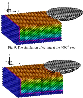
本研究結合 SNOM 奈米級量測實驗及 SNOM 奈米級模擬量測模型,依據第一年模 擬量測所得之結果,逆解出第一隻光纖探針 之幾何尺寸參數,來建出光纖探針原子模型 如圖
2所示,其截斷半徑
r 為 1.2624nm,口c徑為
S=78.4nm。探針尖端凸起高度的大小約是一層 Si 原子所構成的高度 h=0.439nm、共 468 顆原子,斜角為 8.5
0,鍍鋁層厚度
t 為100.6nm。而依據第一隻光纖探針逆解所得之 光纖幾何尺寸模擬所得之結果與進行 SNOM 實驗所得之結果比較如圖
3、圖 4、圖 5與圖
6所示。第一隻光纖探針實驗量測之光纖探 針口徑為 80nm,其與逆解所得之光纖探針口 徑 78.4nm 差距值約為 1.6nm。而實驗的各區 量測值與逆解模擬所得之量測值比較,其之 間的平均誤差為 0.28nm,且實驗量測所得的 鍍鋁層厚度為 100nm 與逆解後所的鍍鋁層厚 度相差約 0.6nm,其差異皆不大,因此可確 認本文所提之逆解光纖探針幾何尺寸之方法 是可行的。而最後為證明本研究所提之逆解 光纖探針幾何尺寸之方法具有可應用到其他 探針的合理性,本研究進行第二隻光纖探針 之 SNOM 奈米級階梯形標準試片量測實驗其 結果如圖
7所示。並逆解出光纖探針的幾何 尺寸,其探針口徑為
S=80.6nm。探針尖端凸起高度的大小為
h=0.451nm 其約可視為一層Si 原子所構成、共 492 顆原子,探針斜角為 8.51
0,鍍鋁層厚度為
t 為 100.9nm。並比較SEM 拍攝的第二隻光纖探針外形如圖
8,與SNOM 實驗所得之量測實驗結果與逆解所得 之模擬結果如圖
9、圖 10、圖 11與圖
12所 示。實驗量測之光纖探針口徑為 82nm,其與 逆解所得之光纖探針口徑 80.6nm 差距值約
為 1.4nm。而實驗的各區量測值與逆解模擬 之量測值比較,其之間的平均誤差為 0.32nm
,且實驗量測所得的鍍鋁層厚度為 101.4nm 與逆解後所的鍍鋁層厚度相差約 0.4nm,其 上述之差異均不大,故可確認本研究所提出 之非破壞方式逆解光纖探針外形尺寸模型為 合理的。
圖1
探針之幾何尺寸關係圖
圖2
逆解後所得之原子模型
3 4 5
15 20 25 30 35 40 45 50 55
階梯形奈米及標準試片
第3區 第2區
第1區
Z(nm)
X(um)
實驗80nm 逆解78.4nm
圖3
第一隻光纖探針逆解後所得 SNOM 模擬
與實驗量測之結果
3.0 3.5 42
44 46 48 50 52
Z(nm)
X (um)
實驗80nm 逆解78.4nm
圖4
第一隻光纖探針逆解後所得 SNOM 模擬 與實驗量測之結果(第 1 區)
3.6 3.8 4.0 4.2 4.4
15 20 25 30 35 40 45 50 55
Z(nm)
X (um)
實驗80nm 逆解78.4nm
圖5
第一隻光纖探針逆解後所得 SNOM 模擬 與實驗量測之結果(第 2 區)
4.4 4.6 4.8 5.0
20 22 24 26
z(nm)
X(um)
實驗80nm 逆解78.4nm
圖6
第一隻光纖探針逆解後所得 SNOM 模擬 與實驗量測之結果(第 3 區)
圖7
第二隻光纖探針 SNOM 實驗量測之結果
圖8
第二隻光纖探針 SEM 實驗所得幾何形貌
4 15
20 25 30 35 40 45 50 55
階梯形奈米級標準試片
第3區 第2區 第1區
Z(nm)
X(um)
實驗82nm 逆解80.6nm
圖9
第二隻光纖探針逆解後所得 SNOM 模擬
與實驗量測之結果
3 40
45 50 55
Z(nm)
X(um)
實驗82nm 逆解80.6nm
圖10
第二隻光纖探針逆解後所得 SNOM 模 擬與實驗量測之結果(第 1 區)
3.7 3.8 3.9 4.0 4.1 4.2 4.3 4.4 4.5
15 20 25 30 35 40 45 50 55
Z(nm)
X(um)
實驗82nm 逆解80.6nm
圖11
第二隻光纖探針逆解後所得 SNOM 模 擬與實驗量測之結果(第 2 區)
4.3 4.4 4.5 4.6 4.7 4.8 4.9 5.0 5.1
21 22 23 24 25 26 27
Z(nm)
X(um)
實驗82nm 逆解80.6nm
圖12
第二隻光纖探針逆解後所得 SNOM 模 擬與實驗量測之結果(第 3 區)
五 、結論
本研究所建立結合二體勢能函數及光纖 探針振動理論之 SNOM 奈米級模擬量測模 型,可分析探討光纖探針不同外形尺寸對 SNOM 奈米級量測之影響,在 SNOM 奈米級 量測具有突破性的重大貢獻。同時透過建立 逆解光纖探針外形尺寸之目標函數值,再結 合數值最佳化 Levenberg-Marquardt Method 最佳化搜尋及合理的收斂準則,可逆解出逆 解光纖探針口徑,並可計算出光纖探針凸起 端尺寸大小,鍍鋁層厚度及斜角。最後比較 SEM 拍攝光纖探針尺寸與 SNOM 實驗量測 奈米級階梯標準試片所得之結果與逆解所得 探針口徑與模擬量測值之結果相比較,其誤 差均不大,故可確認本研究所提出之非破壞 方式逆解光纖探針外形尺寸模型為合理的。
本研究一方面可改善目前光纖探針需破壞才 可得到其幾何尺寸大小之瓶頸。更可作為後 續 SNOM 奈米級量測誤差補償技術之基礎。
六、文獻
1. Tikhonov, A. N. and V. Y. Arsenin, Solution of Ill-posed Problems, V. H. Winston and Sons, Washington, D.C. (1977).
2. Lin, Jiin-Hong, Cha’o-Kuang Chen and Yue-Tzu Yang, “Inverse Estimation of the Thermal Boundary Behavior of a Heated Cylinder Normal to a Laminar Air Stream,”
International Journal of Heat and Mass Transfer, Vol. 43, pp.3991-4001 (2000).
3. Chen, Cha’o-Kuang, Jiin-Hong Lin and Yue-Tzu Yang, “Inverse Method for Estimation Thermal Conductivity in One Dimensional Heat Conduction Problem,”
Journal of Thermophysics and Heat
Transfer, Vol. 15, No. 1, pp. 34-41 (2001).
4. Chang, Win-Jin and Cheng-I Weng, “Inverse Problem of Coupled Heat and Moisture Transport for Prediction of Moisture Distributions in an Annular Cylinder,”
International Journal of Heat and Mass Transfer, 42, pp. 2661-2672 (1999).
5. Romanov, V. G., Cheng-I Weng and Tei-Chen CHen, “An Inverse Problem for a Layered Elastic Plate,” Applied Mathematics and Computation, 137, pp.349-369, (2003).
6. Huang, C. H., M. N. Ozisik and B. Sawaf,
“Conjugate Gradient Method for Determining Unknown Contact Conductance During Metal Casting,” Int. J.
Heat Mass Transfer, Vol. 25, No. 7, pp.
1799-1786 (1992).
7. Balan, T., Lionel Fourment, and Jean-Loup Chenot, “Shape Optimization of the Preforming Tools in forging,” Inverse problems in Engineering: Theory and Practice, ASME, pp.107-113 (1998).
8. Lin. Z. C. and C. K. Chen, , “Inverse Calculation of the Friction Coefficient for Upsetting a Cylindrical Mild steel by Experimental Load”, International Journal of Materials Processing Technology.178, pp.297-306(2006).
9. Schnur D. S. and Zabaras Nicholas, “An
Inverse Method For Determining Elastic Material Properties And A Material Interface,” International Journal for Numerical Methods in Engineering, Vol.33, pp.2039-2057(1992).
10.Ravi,V. and A. A. Jennings, “Penertration Model Parameter Estimate From Dynamic Permeablity Measurements,” Soil Sci. Soc.
Am. J., Vol.54, pp.13-19(1990).
七、計畫成果自評
本研究計畫『近場光學顯微鏡奈米級模擬 量測模型之建立及逆解光纖探針外形尺寸方 法之研究(2/2)』本研究第二年的主要目的是 延續第一年所建立之 SNOM 奈米級模擬量測 模型結合 SNOM 奈米級量測實驗,提出非破 壞方法逆解光纖探針幾何尺寸之方法,解決 光纖探針被破壞而無法繼續使用之技術瓶 頸。並進行第二隻光纖探針 SEM 拍攝工作,
比較 SEM 拍攝與 SNOM 實驗量測所得之結 果與逆解所得之結果的誤差,以確認本研究 所提出之非破壞方式逆解光纖探針外形尺寸 模型為合理的。本研究結果在學理上具有突 破性的貢獻,可於學術期刊發表。而本研究 應用非破壞性方法逆解並計算出光纖探針的 尺寸,亦具有產業應用價值。
本研究執行的成果,已達成原計畫書各項 預期工作項目,其所完成的工作項目概述如 下:
(1)完成第二隻光纖探針量測奈米級階梯標準 試片實驗。
(2)建立逆解光纖探針口徑之目標函數值。及 計算凸起端尺寸大小與鍍鋁層厚度之公 式。
(3)完成逆解光纖探針外形尺寸之模型。
(4)完成逆解出第一隻光纖探針口徑,並計算
凸起端尺寸大小、鍍鋁層厚度及斜角。再
與實驗量測第一隻光纖探針尺寸相比較,證 明本研究之逆解模式為合理的。
(5)完成第二隻光纖探針SEM 拍攝工作,確 認光纖探針口徑及凸起端尺寸大小、鍍鋁 層厚度及斜角。
(6)確認逆解第二隻光纖探針外形尺寸為合理
的,故可證明本研究之逆解模式可重覆應
用於計算其他光纖探針的尺寸。
赴國外研究心得報告
計畫編號 NSC 95-2221-E-011-100-
計畫名稱 近場光學顯微鏡奈米級模擬量測模型之建立及逆解光纖探針外形尺寸方法 之研究(2/2)
出國人員姓名 服務機關及職稱
姓 名:林榮慶
服務機關:國立台灣科技大學 職 稱:教授
出國時間地點
時 間:2006 年 12 月 4 日到 6 日 地 點:新加坡
會議名稱 7
thAsia Pacific Conference on Materials Processing 亞太國際研討會 發表論文題目 3D Nano-scale Cutting Model for Nickel Material
工作記要:
一、參加會議經過
(1)7
thAsia Pacific Conference on Materials Processing 亞太國際研討會,簡稱為 7th APCMP 2006,
其研討會日期為 2006 年 12 月 4 日到 6 日,在新加坡大學舉行,12 月 4 日上午 9 點起開始舉行 開幕儀式及專題演講。同時於上午 11 點起開始舉行各場次研討會。此次會議我被推舉為 11 點 到 12 點 20 分研討會議主持人(Chair) ,並做一場 Session Keynote 的演講,題目為” 3D Nano-scale Cutting Model for NickelMaterial”,其他時間則旁聽其他專家學者的報告。
(2)在第一天下午 3 點多新加坡大學的教授安排參觀新加坡大學機械系設備及研究方向。
(3)此次研討會約有一百多篇論文發表,參加的人有歐洲、美國、日本、韓國、台灣及大陸等學 者。12 月 4 日及 5 日為研討會報告,12 月 6 日大會安埋參觀位於南洋大學的 SIM Tech 實驗 室(由新加坡政府補助)設備及研發成果,進ㄧ步了解新加坡目前的硏發方向。
二、與會心得與建議
此次研討會除了了解目前國際上有關材料加工製程方面的教新研究趨勢外,及由大會所安排的參觀 SIM Tech 實驗室設備及研發成果,整體而言新加坡的發展趨勢和國內大同小異,主要為微型加工及生 醫工程等,但與國內相比新加坡仍較弱,可是由於新加坡小且只有兩間主要大學,因此資源集中使用良 好。
三、建議
每年均需派員參加並補助經費。
三、攜回資料名稱及內容
本次研討會攜回大會所發的研討會論文集光碟ㄧ片以及論文摘要集一本。
3D Nano-scale Cutting Model for Nickel Material
Zone-Ching Lina Jen-Ching Huangb Yeau-Ren Jengc
a Correspondence author, Professor, Department of Mechanical Engineering, National Taiwan University of Science and
Technology, Taipei, Taiwan b Graduate student, Department of Mechanical Engineering, National Taiwan University of Science and Technology, Taipei, Taiwan
c Professor, Department of Mechanical Engineering, National Chung Cheng University, Chia-Yi, Taiwan
Abstract
This paper proposes a method that combines molecular dynamics with finite element deformation model (MDFM) to calculate the stress and strain of a single crystal nickel material that occur during the nano-scale cutting by concial tool. The flow stress-strain curve used in the MDFM model was obtained by nano scale tension simulation using molecular dynamics method in this paper.
Since the Young’s modulus of the nano-scale single crystal nickel material is different from macroscopic scale. Therefore, the Young’s modulus of the single crystal nickel material used in the MDFM model was obtained through a nanoindentation test under very low indentation loading.
The MDFM only requires the elastic-plastic constitutive equation. The position and displacement components of atom in any temporary situation during nano-scale cutting could be found by using the 3-D MD simulation. The atom is regarded as a node and the lattice is regarded as an element. The shape function concept of FEM is applied to calculate the strain of element from atom displacement.
After simulation, it can be found that the accumulation behavior of cutting chip done by nano cutting is quite similar to macroscopic cutting. This paper also finds that residual stress and residual strain will remain on the machined surface of single crystal nickel after cutting.
Keywords: Molecular dynamics (MD), Finite element deformation model, Nano-scale cutting, Nickel.
1. Introduction
In order to understand the properties and mechanisms of nano-scale processing, theoretical analysis is necessary.
Nano-scale processing involves changes in only a few atomic layers at the surface. At such a small governing length scale, the
continuum representation of the problem becomes questionable.
Accordingly, the approach of the molecular dynamics (MD) model is undoubtedly needed to trace the behavior of atoms with the short-range interaction during short-time scale.
MD simulation studies, in general, were initiated in the late 1950’s by Alder and Wainwright [1] in the field of statistical mechanics. Based on the MD simulation, Maekawa and Itoh [2]
and Zhang and Tanaka [3] conducted MD analyses of processing and friction characteristics of ultra-precise cutting on the atomic scale. These analyses were based on a two-dimensional (2D) model to reduce the calculation time. 3D MD analysis is required to provide a deep insight into nano cutting. Isono and Tanaka [4]
carried out a 3D MD analysis of the effects of temperature, machinability and interatomic force on nickel metal.
The application scope of FEM is rather extensive. Thus, many scholars propose to combine FEM and MD methods to study the distribution of macroscopic and mesoscropic stress and different phenomena. As proposed by Izumi [5], an integration of FEM and MD could be applied to investigate the elastic deformation behavior of Si in times of stretching. His method was to divide the simulation space into 4 zones, and suggested the corresponding data adjustment of the two-layer transformation (transition) zone between FEM zone and MD zone. P. Liu et al [6]
mentioned an atomistic and continuum concurrent model to study the stress distribution of epitaxial island at elastic stage.
Epitaxial island was simulated by MD, whereas substrate was simulated by FEM. There was an overlapping zone between them so as for atomistic and continuum models to exchange necessary material information.
It can be known from the above discussion that the combination of FEM and MD in literatures mostly divides simulation space into 3 zones: one is the atomistic scale MD simulation zone, one is the FEM calculation zone of macroscopic continuum model, and the last is the transition zone, i.e. the interface zone between MD simulation zone and FEM calculation zone. However, it can not directly apply the abovementioned combination of FEM and MD to analyze the stress and stain of each axis in the MD zone during nano-scale cutting. Therefore, over the combination of FEM and MD simulation techniques in solving the problem of nanoscale cutting mechanism, there are still worth to be studied.
Lin and Huang [7] directly regarding the atom as a node, and the lattice as an element, Lin and Huang suggested a way that combined FEM shape function concept and MD techniques to calculate the equivalent stress and equivalent strain of single crystal copper caused by three dimensional nano-scale cutting.
However, Lin and Huang [7] only calculated the equivalent stress and equivalent strain of the cross-section of workpiece based on the plane strain condition during nano-scale cutting, with no finite deformation theory imported. Thus, the effects of the shape change and rotation of element were not considered. Accordingly, various axial stress and strain of workpiece could not be acquired. Since the condition of residual strainand residual stress of machined surface will tremendously affect
the follow-up processing and applicability, it is extremely necessary to be developed an analyzable and calculable residual strain and residual stress model of machined surface.
This paper proposes a method that combines molecular dynamics with finite element deformation model (MDFM) to calculate the various axial stress and strain of single crystal nickel that occur during nano-scale cutting by conical tool. This paper also employs rigid boundary layer interface force (RIF) model developed by Lin and Huang [8] to calculate the cutting force of single crystal nickel during nano cutting.
2. Molecular dynamic simulation of nano-cutting 2.1 Nano-cutting simulation model
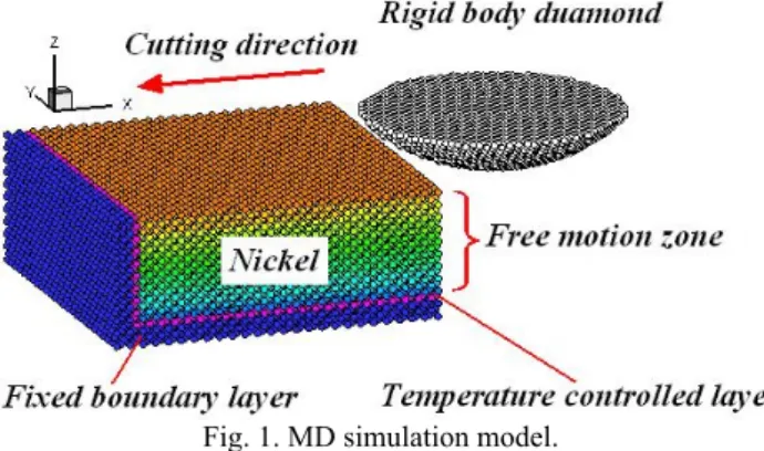
In this study, a workpiece and a tool are assumed to consist respectively of single crystal nickel and rigid diamond, as shown in Figure 1 and Table 1. To simulate the nano-scale cutting of the (001) plane of nickel, we utilize a nickel slab of dimensions 25a × 25a × 11a, consisting of 27500 atoms (Figure 1), where a is the lattice constant of nickel (3.52 Å)[4].
The work material in the MD simulation is divided into three different zones, namely the free motion zone,temperature controlled layer and the fixed boundary layer [7].
Fig. 1. MD simulation model.
The boundary conditions of nano-scale cutting simulation included the three layers of atoms in the y-z faces (left side of the work material) and the lower x-y plane (bottom of the work material) being kept fixed [7]. All other atoms are allowed to move with the MD algorithm.
A layer of atoms at the free motion zone and close to the fixed boundary layer are considered as thermostat atoms. In another word, the layer of atoms at the free motion zone and close to the fixed boundary layer is considered as a temperature controlled layer. The temperature controlled layer was used to absorb the heat towards primary cells.
Table 1 Computational parameters used in the MD simulation
Configuration Nano cutting
nickel (Work material ) 25a×26a×10a, atoms: 27311 Tool (rigid body diamond) Tip radius: 5nm
total tool atoms:15400 Depth of cut 0.55nm Cutting speed 200 m/sec Bulk temperature 293 K
In typical metal machining conditions, a nickel surface is machined by a considerably harder tool or abrasive element.
The hardness of diamond is 10, whereas nickel is considerably softer (hardness < 5 ) depending on the surface preparation [9].
Under such conditions it is a good approximation to consider the tool as a rigid body. We adopt this convention in these simulations.
When using MD to simulate the tool having a radius of cutting edge to undergo nano-scale cutting, the deeper the cutting depth, the larger the size of the workpiece would become. In other words, when there are lots of atoms in a
workpiece, the volume of calculation would relatively be massive in times of simulation. When Zhang and Tanaka [3]
used MD to undergo nano-scale cutting simulation, they found that when the proportion of cutting depth versus the radius of the tip is larger or equal to 0.09, then the condition of nano-scale cutting is equivalent to the cutting regime. The radius of cutting edge in this paper is 5 nm, and hence, the cutting depth is larger or equal to 0.45 nm (i.e., the cutting regime) only. The simulated cutting depth in this paper is 0.55 nm. Such a cutting depth can be used to investigate the cutting regime, whereas its time of calculation is also affordable.
2.2 MD simulation
In this study, the face center cubic structure of single crystal nickel is established as the experimental samples. The Gear’s predictor-corrector method is adopted to calculate the positions, velocities and accelerations of particles under displacement condition. The both Verlet’s neighbor lists [10]
and truncated radius method [10] are employed to reduce plenty of calculative quantities.
The MD simulation procedure in this study is based on the references [10,11]. Initially, the atoms of the specimen are positioned at the fcc lattice sites, then relaxed to the equilibrium position after the nano-scale cutting was applied.
The MD simulations were carried out in the specimen of the nickel. Therefore, in this study, the MD simulation comprises two phases: initial relaxation and machining. In the first phase, atoms were positioned according to an assumed face-centred-cubic (fcc) crystal structure and their velocities were randomized to satisfy the Maxwell-Boltzmann distribution at prescribed temperature [10,11]. For the simulation results presented below, the relaxation phase was completed within 20000 time steps by controlling the bulk temperature at a 293K using an NVT ensemble [10,11]. In the second phase, nano-scale cutting was simulated by displacing the diamonod tool with small distance (interval) toward the negative direction of X-axis in each time step, and followed by relaxation for 500 MD steps (cutting). Further details of MD simulation procedure are given in [10,11].
In this paper, the Morse potential model function, which is still widely used, is also adopted for the calculation process. It is
( ) ( )
{
02
0}
)
(
rij=
D⋅
e−2αrij−r−
e−αrij−rφ (1) where φ(rij ) is a pair potential energy function, D is the
cohesion energy,αis the elastic modulus and r0 is the particle distance at equilibrium. The shape of the potential function s and their related parameters are shown in Table 2.
Table 2 Parameters of Morse potentials [4]
Parameter Ni- Ni Ni -C
D(eV) 0.4205 0.100
α (1010m-1) 1.4199 2.200
r0(10-10m) 2.78 2.40
To ensure reasonable heat conduction outwards the control volume (primary cell), a temperature-controlled layer was used to absorb the heat towards primary cells. At nano-scale cutting simulation, when temperature of the temperature absorption layer is higher than the preset one of 293K, velocity rescaling method as shown in Equation (2) [10] will be used to control the temperature of the temperature controlled layer and absorb the heat towards primary cells (control volume). Converting the average kinetic energy into a temperature as shown in Equation (3) [10] does conversion of temperature for thermostat atoms. Successful application of Equation (3) can be found in prior works such as Lin and Huang [7,8].
A D i new
i T
v T
v, = (2)
∑ ⋅
=
i i i
A N
T v v
3
1 (3)
Where vi,new is the velocity of the particle i after correction.
TD and TA are the desired temperature and actual temperature of system, respectively. N is the total number of temperature-controlled layers.
3. Calculation of atomistic strain and atomistic stress
3.1 Calculation of atomistic strain
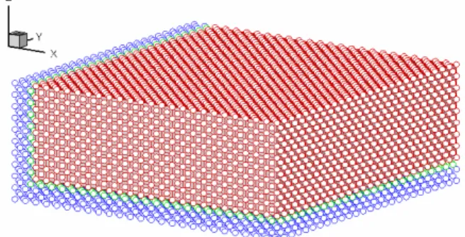
The atomic lattice array was considered in the combined molecular dynamics and finite element deformation model (MDFM) to calculate the stress and strain in the nano-scale cutting. Every atom position has its physical meaning since the MD calculation is based on each atom. The calculation result of each step in MD will be influenced by the existence of each atom. Therefore, concerning the influence of each atom to the whole system, every atom was considered as a node to investigate the nano-scale cutting behavior in this article.
The solid element of constant strain tetrahedron (CST) was selected in this study. Every FCC unit lattice at free motion zone was meshed 24 CST elements. The model of finite element separation is shown in Figure 2. Thus, in this article, it takes CST element and combining MD with FEM shape function, the finite deformation model of nano-scale cutting can be constructed. The relationship among the displacement field, strain field and node displacement of single CST element can be expressed as follows [12]:
{ }
uˆ e =[ ] { }
N e d e (4){ } ε
e =[ ] { }
Bε e d e (5) In which, { }uˆ is the displacement field inside the element, e{ }deis the node displacement of element, { }ε e is the strain field inside the element,
[ ]
B is the strain-displacement matrix, ε and[ ]N is the shape function. Their values are shown in [12].The deformation of nano-scale cutting element is very great, exceeding the elasticity and entering plasticity. Thus, in the strain calculation, this paper employs the displacement increment from the previous step to the current step to calculate the strain increment, and also uses ULF (updated Lagrangian formulation) [13] physical field to calculate strain increment.
Fig. 2. Model of element mesh of MDFM.
3.2 Calculation of atomistic stress
A linear relationship is established between stress
increment
{ }
dσ and elastic strain increment{ }
dε while e isotropic material is deformed within its elastic range, i.e.satisfying Hook’s law. The matrix expression is given by
{ }
dσ =[ ]
De{ }
dεe (6)where,
{ } {
x y z xy yz xz}
T d d d d d d
dσ : σ σ σ σ σ σ ,
[ ]
De :relationship matrix of elastic stress and strain,{ }
{
x y z xy yz xz}
T d d d d d d
dε : ε ε ε ε ε ε
During cutting, the element will be changed in shape and rotated. Thus, this paper employs finite deformation theory [13], ULF physical field [13], and also nano-scale flow curve and strain-hardening rate to derive the elastic-plastic relationship equation of nano-scale finite deformation theory. Therefore, when the stress induced by the deformation of workpiece reaches the yield condition, the plastic deformation of workpiece would occur and the elastic-plastic relationship of stress and strain equation can be indicated as:
{ }
dσ
=[ ]
Dep{ }
dε
(7)where
{ }
dε denotes the matrix of total strain increment, [ ] [ ] [ ] [ ][ ] ⎭⎬⎫
⎩⎨
⎧
∂
∂
⎭⎬
⎫
⎩⎨
⎧
∂ + ∂
′
⎭⎬
⎫
⎩⎨
⎧
∂
∂
⎭⎬
⎫
⎩⎨
⎧
∂
∂
−
=
σ σ
σ σ
D f H f
f D D f D D
e T
e T e
e
ep , H ′ is the strain hardening rate
and f is the plastic potential.
After derivation and simplification, the elastic-plastic relationship equation of nano-scale finite deformation of the increment form is:
{
Δσ
J}
=[ ]
Dep{ }
Δε
(8) where{
ΔσJ}
is the increment form of the Jaumanndifferential of Euler stress[13].
And, the increment form of real stress (Euler stress) be obtained as follows:
[ ] [
Δσ = ΔσJ] [ ] [ ] [ ][ ]
− ΔT T σ −σ ΔT (9) where,[ ]
ΔT is a coordinate transformation matrix.
Therefore, the real stress (Euler stress)
{ }
σt+Δt of everyelement can be obtained under the time t+△t by Equation (10).
{ } { }
σt+Δt = σt +{ }
Δσ (10) Then, by using strain increment, the stress increment canbe calculated by the elastic-plastic relationship equation of nano-scale finite deformation theory.
In times of elastic and plastic deformation of nickel material, its Poisson’s ratio is a important parameters. This paper quotes the Poisson’s ratio, being 0.31 [14].
3.3 Flow curve of nano-scale single crystal nickel
For convenience of calculation and analysis, many scholars have proposed that, based on the result of the stretching experiments of materials, a stress-strain equation at times of plastic deformity can be obtained. This equation is known as a flow curve equation. Therefore, this study uses the
stress-strain curve of a nano-scale nickel thin film tension test simulation by Chen [15] as a base. The stress-strain curve will be regressed and converted into a flow stress-strain relationship equation. The unit of the flow curve is GPa (N/mm2).
σ = 58.33655 ε0.99247 (11) 3.4 The Young’s modulus of single crystal nickel
In times of elastic and plastic deformation of nickel material, its Young’s modulus is a important parameters. Thus, it is very important to choose the suitable Young’s modulus during simulation.
Since the Young’s modulus of the nano-scale single crystal nickel material is different from macroscopic scale. Therefore, the Young’s modulus of the single crystal nickel material used in the MDFM model was obtained through a nanoindentation test under very low indentation loading.
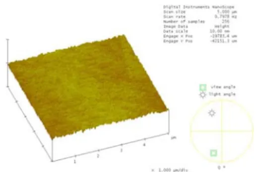
The single crystal nickel used in this paper is produced by MaTeck Company of Germany. Its orientation accuracy is <
0.1° and its surface roughness is 0.302nm (Ra). Its surface topography is shown in Figure 3.
Fig. 3. The surface topography of Ni single crystal This paper uses TriboScope equipment produced by Hysitron Inc. to undergo very low indentation loading experiment on the (001) surface of single crystal nickel by means of Berkovich’s Indenter. As shown in Figure 4, the total included angle on this tip is 142.3°, with a half angle of 65.35°.
This tip geometry has been used as the standard for nanoindentation [16].
Fig. 4. SEM photo of Berkovich’s Indenter
The load used in this paper ranges from 75μN, 100μN, 125μN to 150μN. Every loading is indented for six times to ask for its average value, so as to avoid experimental error.
Figure 5 shows the depth and loading of indentation experiment and Figure 6 shows the surface topography after indentation.
(a) 75μN
(b) 150μN
(c) 200μN
Fig. 5. Depth and force curve of the indentation experiment
(a)75μN (b)100μN
(c) 150μN
(d) 200μN
(e) 250μN
Fig. 6. Surface topography of single crystal Ni after indentation
From Figure 5, it can be seen that the machine used in this paper can still work steadily under the indentation experiment having an extremely low loading. Also from Figure 6, the topography of the indentation would enlarge along with the increase of the loading of the indenter. Therefore, the Er obtained in this experiment is very reliable. Figure 7 shows the relation between the indentation depth and Er after experiment, and the average value of Er acquired in this paper is 219.89 GPa. The Er value is further converted into Young’s modulus through the following equation[16], and the value is