藉由時域聚焦多光子激發術於高通量微結構之製作
112
0
0
全文
(2)
(3) Abstract In this thesis, multiphoton excitation (MPE) microfabrication using Rose Bengal (RB) as the photoinitiator was first used to create two-dimensional (2D) micropatterns and three-dimensional (3D) microstructures with various materials, such as extracellular matrix (ECM) proteins, gelatin, and polymer, and then utilized the bio-microstructures to guide axonal outgrowth of primary cortical neurons. Large-scale positive and negative patterns were created, and the results demonstrated that neurite growth can be constrained or guided in a well-controlled manner via the micropatterns. In addition, gelatin, a denature collagen or mixture of gelatin and poly-D-lysine (PDL) were used for fabricating 3D microstructures. The results are also promising for guiding growth of axons in 3D microenvironment. However, one of the limits of conventional scanning MPE microfabrication is its low throughput due to point-by-point processing. To surpass this limit, a MPE microfabrication system based on temporal focusing and patterned excitation has been developed to quickly provide 3D freeform polymer microstructures. The microstructures are created by sequentially stacking 2D fabricating patterns. Compared to conventional scanning MPE, this approach offers freeform microstructures and a greater than three-order increase in fabrication speed. Furthermore, the system integrated with a digital micromirror device for locally controlling the laser pulse numbers which can provide high-throughput fabrication of 3D gray-level bio-microstructures via. I.
(4) two-photon crosslinking. Multiple bovine serum albumin (BSA) structures of different concentrations were simultaneously achieved by selecting different pulse numbers in the designated regions with an appropriate femtosecond laser power within a few seconds. Moreover, the fabricated BSA microstructure can be monitored online by utilizing the RB two-photon excited fluorescence (TPEF) as contrast agent. This approach with its unique capability of high-speed,. gray-level,. and. online-inspection. fabrication. meets. the. requirements of the biomedical researches involved in ECM. Finally, high-throughput multiphoton-induced reduction and ablation of graphene oxide (GO) films has also been studied using this system. The degree of reduction and ablation can be precisely implemented via controlling the laser wavelength, power, and pulse number. Compared to point-by-point scanning laser direct writing, this method offers a high-throughput and multiple-function approach to accomplish large-area and micro-scale patterns on GO films. The high-throughput micropatterning of GO via the temporal focusing-based femtosecond laser system matches the requirement of mass production for GO-based applications in microelectronic devices.. Keywords: multiphoton excited microfabrication, neuronal guidance, extracellular matrix, temporal focusing, multiphoton-induced ablation. II.
(5) 摘 要 本論文一開始,以孟加拉玫瑰素(rose Bengal,RB)當作光起始劑之多光子 激發(multiphoton excitation,MPE)微製作技術被用來製作各種材料之二維 微米圖案及三維微米結構,例如細胞外基質(extracellular matrix,ECM) 蛋白質、明膠和高分子聚合物,並利用它們來引導小鼠大腦皮質神經細 胞的軸突生長。實驗結果顯示,神經軸突的生長可以很有效率的被侷限 或引導藉由這些大面積的二維正向和負向微米圖案,同時也探討了不同 材料對於神經軸突生長的影響。除此之外,我們亦使用了另一種變性膠 原蛋白材料-明膠,或明膠與多聚賴氨酸(poly-D-lysine,PDL)的混合液 來製作具生物相容性的三維微米結構。其結果亦顯示這些微結構對於引 導神經軸突在三維環境的生長是很有潛力的。 然而,由於傳統的 MPE 微製作技術是採用點掃描的方式來進行,因 此、製作速度慢所造成的低產量是其最大缺點。為了改善這個限制,我 們發展了一套具時域聚焦與圖形化照射的 MPE 微製作系統。藉由一層一 層堆疊的方式,任意形狀的三維高分子聚合物結構可以被快速地製作出 來。與傳統的掃描式 MPE 相比,此方法不僅可製作出任意形狀的微結構, 在製作的速度上更可提升約三個數量級。此外,這套系統整合了一個數 位微面鏡裝置(digital micromirror device)可用來針對特定的區域,局部地 控制雷射脈衝的數量。藉由這項功能並搭配 RB 當作光活化劑,多個不同 灰階(梯度濃度)的三維牛血清蛋白(bovine serum albumin,BSA)結構可以 在幾秒鐘之內被同時製作出來。同時,所製作出來的牛血清蛋白結構亦 可被即時監測藉由利用 RB 當作雙光子激發螢光(two-photon excited fluorescence,TPEF)的對比劑。因具有獨特的高速、灰階製作以及即時監 III.
(6) 控的能力,此方法符合了許多生醫應用的需求,特別是對於細胞外基質 的相關研究。 最後,我們亦利用此系統對氧化石墨烯(graphene oxide,GO)薄膜進 行高通量多光子誘發還原與剝離的研究。還原的程度以及剝離的過程可 以很精準地被操控藉由調控雷射的波長、功率以及脈衝數量。相對於逐 點雷射掃描的方式,此方法具備了高產能與多功能的優點,進而可以在 GO 的薄膜上製作出具有微米特徵尺度的大面積圖案。因此,此具有時域 聚焦與脈衝控制的超快雷射系統可符合高產量的需求,將有助於 GO 相 關材料在微電子裝置上的應用。. 關鍵字: 多光子激發微米製作、神經引導、細胞外基質、時域聚焦、多 光子誘發剝離。. IV.
(7) Acknowledgements 自從大學作專題開始到現在的博士班畢業,回首待在這實驗室的時間也 已經過了七年多。很高興可以在這裡認識了許許多多的好朋友、同時也 從他們的身上學到了很多。所幸在經歷了這漫長的研究與等待,最後終 於得以順利地完成本論文。首先、我要感謝我的指導教授陳顯禎 博士, 在我還是一個對光學懵懂的大三學生時,一手把我帶入這陌生的領域, 並用其豐富的學術涵養不厭其煩的教誨我。雖然在這期間我們偶爾會有 意見分歧的時候,但感謝老師總是能從旁曉以大義,支持並信任我們所 做的決定。碩班畢業時,在您的大力鼓勵下展開了未知的博士班生涯, 當時的我並不知道這到底是好還是壞,但回顧這五年的點點滴滴與現在 的結果看來,我很慶幸當時的那個決定以及有您一路以來的引導與協助。 另外,也要感謝各位口試委員的指導與糾正,才能讓此論文更臻完備。 博士班期間受到實驗室許多人的幫忙,感謝林俊佑學長在理論與模 擬上的指導與建議,不經意的一句話常常就可以讓我們豁然開朗。謝謝 邱國智學長和卓粳佶學長在實驗上的幫忙,以前儀器有問題時總是要向 你們求救。感謝同屆的蘇宏瑋同學在早期實驗系統發展上的幫忙。另外 也要感謝張家源學弟在程式撰寫上投下的心力,讓我們可以有非常“友 善”的儀器使用者介面,還有鄭力中學弟、李育杰學弟、胡瑜凌學妹、 張芯語學妹以及李家葳學弟除了學術研究上的協助之外,還提供了許許 多多茶餘飯後的生活趣事,讓這有點乏味的研究生生活頓時增添了不少 樂趣。最後也要感謝連啟翔學弟在我剛到美國時在生活上給予我的幫助, 讓我可以快速地適性當地生活。 除此之外、還要感謝科技部的千里馬計畫以及 Prof. Paul Campagnola V.
(8) 提供給我這個機會,讓我可以到 UW-Madison 進行 11 個月的研究學習。 那段期間裡,除了謝謝 Prof. Paul Campagnola 與 Prof. Justin Williams 的指 導之外,也要感謝 Visar Ajeti 同學在實驗上與生活上的協助,才能有目 前本論文 Chapter 2 的研究成果。另外也要感謝當時的兩位“廚師”-我 的室友成祥和女朋友婷妮,讓我在美國可以不愁吃。真的很高興在博士 班生涯的最後階段能到國外體驗不一樣的生活、結交不同生活圈的好朋 友,在那裡的點點滴滴不僅豐富了本論文,也留給我許多無可取代的美 好回憶。 最後,我要感謝一路以來一直在背後默默支持與鼓勵我的父母以及 姊姊,謝謝你們總是無怨無悔的信任我做的每個決定,沒有你們的付出 與照顧就不會有現在的我。謹以此文獻給我的家人、以及在這二十幾年 的求學生涯中所遇到的師長與朋友,謝謝你們!. VI.
(9) Table of Contents Abstract............................................................................................................... I 摘 要 ............................................................................................................... III Acknowledgements .......................................................................................... V Table of Contents .......................................................................................... VII List of Figures .................................................................................................. X Abbreviations ..............................................................................................XVII Chapter 1 Introduction....................................................................................... 1 1.1 Introduction ......................................................................................... 1 1.2 Motivation ........................................................................................... 7 1.3 Outline ................................................................................................. 8 Chapter 2 Extracellular Matrix for Guidance of Neuronal Growth ................ 10 2.1 Introduction of axonal guidance........................................................ 10 2.2 Multiphoton excited polymerization and crosslinking ..................... 12 2.3 Sample preparation and neuron culture ............................................ 16 2.4 Experimental setup and results.......................................................... 19 2.4.1 Optical setup and instrument control ..................................... 19 2.4.2 Neuronal growth on 2D micropatterns................................... 20 2.4.3 3D microstructures for axonal guidance ................................ 33 Chapter 3 Temporal Focusing-based Fabrication of Polymer Microstructures ......................................................................................................................... 38 3.1 Temporal focusing-based multiphoton excitation ............................. 38. VII.
(10) 3.2 System setup and sample preparation ............................................... 41 3.2.1 High-throughput multiphoton microfabrication system ........ 41 3.2.2. Designing 3D freeform structures and sample preparation .. 44 3.3 Experimental results and discussions ................................................ 45 3.3.1 System calibrations ................................................................ 45 3.3.2. Fabrication. and. inspection. of. freeform. polymer. microstructures ................................................................................ 49 Chapter 4 High-throughput Fabrication of Gray-level Bio-microstructures .. 53 4.1 Introduction ....................................................................................... 53 4.2 Sample preparation and microfabrication setup................................ 55 4.2.1 High-throughput gray-level microfabrication system............ 55 4.2.2 Bio-monomer preparation ...................................................... 57 4.3 Experimental results and discussions ................................................ 57 4.3.1 System calibrations ................................................................ 57 4.3.2 Online imaging and inspection of BSA microstructures ....... 62 4.3.3 3D gray-level BSA microstructures ....................................... 64 Chapter 5 Multiphoton-induced Reduction and Ablation of Graphene Oxide Micropatterns................................................................................................... 68 5.1 Multiphoton-induced ablation ........................................................... 68 5.2 Sample preparation ............................................................................ 70 5.3 Experimental results and discussions ................................................ 72 5.3.1 Wavelength selection for multiphoton-induced reduction & ablation ............................................................................................ 72. VIII.
(11) 5.3.2 Manipulate the degree of reduction via pulse number control ......................................................................................................... 73 5.3.3 Freeform micropatterning of GO film at different power and pulse number ................................................................................... 76 Chapter 6 Conclusions .................................................................................... 80 References ....................................................................................................... 82 Curriculum Vitae ............................................................................................. 89. IX.
(12) List of Figures Figure 2-1 Jablonski diagram of RB with two-photon excitation. ............... 14 Figure 2-2 (a) Primary rat/mouse cortical neurons; (b) sample preparation for cell culture; and, (c) time-lapse microscope with an automatic temperature, CO2, and humidity controller. ................................ 18 Figure 2-3 Optical configuration of the fabrication system, incorporating separate EOMs for power control and rapid shuttering and an FPGA for control of the fabrication process [66]....................... 20 Figure 2-4 Rat cortical neurons cultured on FN fibers with line width of 1 μm and periodicity of 10 μm at different time state. (a) t=9 hours; (b) t=15 hours; (c) t=27 hours, and (d) t=36 hours. ......................... 22 Figure 2-5 Island-bridge (a) positive and (b) negative patterns. Neurons cultured on negative patterns for 3 days (c) & (d), and 5 days (e) with materials of (c) BSA, (d) TMPTA, and (e) gelatin, respectively. ................................................................................ 23 Figure 2-6 Positive island-bridge pattern of (a) FN with concentration of 1 mg/ml; (b) FN/BSA mixture with concentration of 500 μg/ml and 100 mg/ml, respectively; (c) LN/BSA mixture with concentration of 50 μg/ml and 100 mg/ml, respectively. .................................. 23 Figure 2-7 (a) Phase contrast image of rat cortical neurons after 36 hours of culture on PLL positive patterns. (b) Corresponding fluorescence image at the same position as (a). ............................................... 25 Figure 2-8 (a) Combination of phase contrast image and fluorescence image X.
(13) of neurons which were cultured on FITC-PLL positive patterns for 72 hours. (b) Phase contrast image of neural network after 108 hours culture on PLL positive patterns................................ 26 Figure 2-9 Neurons cultured on LN patterns with PDL background for 48 hours. (a) Stripe patterns with periodicity of 24 μm and 12 μm; (b) & (c) Stripe patterns with periodicity of 6 μm and 4 μm; (d) Positive island-bridge patterns. .................................................. 28 Figure 2-10 (a) Phase contrast images of patterned FITC-PLL monolayer via MPE etching. Inset: corresponding fluorescence images. (b) Mouse cortical neurons cultured on 2D freeform pattern for 120 hours. (c) Corresponding fluorescence images of (b). Inset: designed pattern for etching. ...................................................... 28 Figure 2-11 Fluorescence images of large-scale antibody stained LN monolayer with designed pattern which was etched by MPE photochemistry. .......................................................................... 31 Figure 2-12 Phase contrast images of ovarian cancer cells which were cultured on LN monolayer for 24 hours with the patterns of (a) “Nature” words, (b) stripes with periodicity of 12 & 24 μm, and (c) positive island-bridge. Inset: corresponding designed patterns for etching. .................................................................................................... 31 Figure 2-13 Cortical neurons cultured on patterned L1+PDL surfaces for 120 hours which were fabricated by MPE etching............................ 32 Figure 2-14 Phase contrast images of neurons cultured on positive. XI.
(14) island-bridge patterns of L1+PDL for 120 hours with gaps of (a) 10 μm and 20 μm; (b) 30 μm and 50 μm. ................................... 32 Figure 2-15 (a) Top view, and (b) bottom view of 3D microchannel structures with hole diameter of 15 μm, channel width of 5 μm, and height of 25 μm. (c) Scheme of 3D microgroove-bridge structures with groove width of 12 μm, and height of 20 μm. ............................ 34 Figure 2-16 Phase contrast images of neurons cultured on 3D microchannel arrays with PDL background for 72 hours. ................................ 35 Figure 2-17 Phase contrast images of neurons cultured on 3D microstructures of (a) gelatin only for 72 hours; (b) & (c) mixture of gelatin and PDL for 40 hours. All of the structures were fabricated on PDL monolayer. .................................................................................. 36 Figure 2-18 Phase contrast image of neurons cultured on cone-shaped structures for 72 hours with bottom diameter of 90 μm, top diameter of 10 μm, step size of 3 μm, and height of 20 μm. Inset: Scheme of 3D micro-cone structures. ........................................ 37 Figure 3-1 Schematic diagrams of the concept of spatial focusing and temporal focusing [67]................................................................ 39 Figure 3-2 Graphically demonstrates the principle of depth-resolved widefield illumination................................................................. 40 Figure 3-3 Optical. setup. of. the. high-throughput. multiphoton. microfabrication system based on spatiotemporal focusing and patterned excitation..................................................................... 43. XII.
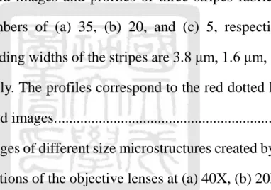
(15) Figure 3-4 (a) Normalized TPEF intensities of fabricated solution as a function of different gray levels of the DMD. (b) Bright-field images of 5 different sizes of TMPTA polymer microstructures with the use of three different laser powers at 12.2 mW, 8.7 mW, and 5.2 mW (from top to bottom) corresponding to the minimum demanded gray levels, respectively. Sizes of the fabricated squares are respectively 42 μm, 33 μm, 23 μm, 14 μm, and 8 μm (from left to right). ...................................................................... 47 Figure 3-5 Bright-field images and profiles of three stripes fabricated with pixel numbers of (a) 35, (b) 20, and (c) 5, respectively. The corresponding widths of the stripes are 3.8 μm, 1.6 μm, and 1 μm, respectively. The profiles correspond to the red dotted line in the bright-field images. ..................................................................... 48 Figure 3-6 TPEF images of different size microstructures created by different magnifications of the objective lenses at (a) 40X, (b) 20X, and (c) 10X. The heights of three structures are all 30 μm. ................... 50 Figure 3-7 3D renderings of the TPEF images of the excitation patterns during the high-throughput microfabrication process: (a) pyramid structure and (b) multiple objects (triangle, star, rectangle, and circle) with different heights. Inset: 2D front-view bright-field images. ........................................................................................ 52 Figure 3-8 3D renderings of the TPEF images of the fabricated microstructures in Fig. 3-7(b) after washing the remaining. XIII.
(16) solution using: (a) typical scanning multiphoton microscope, and (b) multiphoton microfabrication system with only the widefield microscopy function. .................................................................. 52 Figure 4-1 Optical setup of the high-throughput gray-level multiphoton microfabrication system based on temporal focusing excitation. .................................................................................................... 56 Figure 4-2 (a) Normalized TPEF intensity as a function of different pulse number under the gated mode operation. Fluence of each pulse is 35 μJ. (b) Relationship between the normalized TPEF intensity and the DMD gray-level with gated mode operation to control the global pulse number of 1000. ..................................................... 61 Figure 4-3 TPEF images and profiles of two stripes fabricated with the pixel numbers of (a) 46 and (b) 23, the fabricated widths of which are 2.3 μm and 1.1 μm, respectively. The profiles correspond to the red dash line in the TPEF images. Inset: corresponding 2D front-view bright-field images. ................................................... 61 Figure 4-4 TPEF images of the fabricated multi-object BSA microstructures. (a) Widefield imaging before washing out the remaining solution. (b) Image acquired via conventional point-scanning microscopy after washing out the remaining solution. (c) Figure 4-4(b) image acquired after adding match oil. Inset: corresponding 2D front-view bright-field images. ................................................... 64 Figure 4-5 Images and profile of the RB TPEF intensity in the crosslinked. XIV.
(17) BSA microstructures fabricated by globally and locally selecting the pulse numbers: (a) designed gray-level pattern of 2 × 3 squares (each square measures 12 × 12 μm2) from the highest level of 255 to the lowest level of 127 via the DMD, (b) the corresponding TPEF image of the fabricated gray-level BSA micro-squares, and (c) profile corresponding to the red dash line in Fig. 4-5(b). .............................................................................. 67 Figure 4-6 TPEF images of the fabricated gray-level multi-object BSA microstructures via: (a) the multiphoton lithography system before cleansing the remaining solution, and (b) the conventional point-scanning multiphoton microscope and (c) the multiphoton lithography system, both after washing out the unreacted solution and injecting match oil. .............................................................. 67 Figure 5-1 Schematic diagram of optical breakdown. (a) A free electron is excited from valence band to conduction band via MPI process; (b) The electron linearly absorbs few photons until its energy reaches twice of the binding potential, and then impact ionizes the other bound electron [68]. .................................................................... 70 Figure 5-2 Schematic diagram of the preparation of GO from graphite power by modified Hummers method. .................................................. 71 Figure 5-3 The top row is the bright-field images of the reduced/ablated squares using the laser wavelength of 830 nm at different powers of 50 mW, 60 mW, 70 mW, 80 mW, and 90 mW, respectively. XV.
(18) (left to right). The bottom row is the images at 750 nm wavelength. Laser powers are adjusted as 10 mW, 20 mW, 30 mW, 40 mW, and 50 mW, respectively (left to right). ..................................... 73 Figure 5-4 (a) Bright-field images of reduced GO squares at different pulse number. The pulse number is labeled at left-top corner. (b) Six micro-Raman spectra correspond to the six reduced patterns in Fig. 5-4(a), respectively without baseline correction and with baseline correction (c)............................................................................... 76 Figure 5-5 Bright-field images of rGO-based disk arrays processed at pulse energy of 2.2 μJ: (a) the disks with the diameter of 5 μm by illuminating 10000 pulses; and, (b) the disks with the diameter of 3 μm by 10000, 15000, and 20000 pulses (top to bottom), respectively. ................................................................................ 78 Figure 5-6 Bright-field images of GO film with reduction/ablation: (a) ablation only, and (b) reduction first and then ablation. Inset of Fig. 5-6(b): bright-field image of the reduced square before ablation. .................................................................................................... 79. XVI.
(19) Abbreviations BSA. bovine serum albumin. CCD. charge coupled device. DMD. digital micromirror device. DAQ. data acquisition. ECM. extracellular matrix. EOM. electro-optic modulator. FN. fibronectin. FRET. Förster resonance energy transfer. FBS. fetal bovine serum. FPGA. field programmable gate array. FIFO. first-in first-out. GO. graphene oxide. LN. laminin. MPE. multiphoton excitation. MPA. multiphoton absorption. MPI:. multiphoton ionization. µRS:. micro-Raman spectroscopy. μCP. microcontact printing. NA. numerical aperture. NIR. near infrared. PM. plating medium. PLL. poly-L-lysine XVII.
(20) PDL. poly-D-lysine. PBS. phosphate buffered saline. PMT. photomultiplier tubes. RB. rose Bengal. rGO. reduced graphene oxide. SHG. second harmonic generation. SFM. serum-free medium. STL. stereo-lithography. ti-sa. titanium-sapphire. TPA. two-photon absorption. TMPTA. trimethylolpropane triacrylate. TPP. two-photon polymerization. TPC. two-photon crosslinking. TPEF. two-photon excited fluorescence. TEA. triethanolamin. XVIII.
(21) Chapter 1 Introduction 1.1 Introduction In 1990s, the advent of ultrafast laser technology has enabled the observation of the nonlinear optical processes that occur when electric field interacts strongly with materials. With superior features such as deeper penetration depth, lower photobleaching, and minimum invasion, multiphoton excitation (MPE) fluorescence microscopy is particularly suitable for imaging thick tissue and living animals [1]. Additionally, second harmonic generation (SHG), another phenomenon of nonlinear optics, can be employed to directly obtain contour information of non-centrosymmetry within specimens without labeling [2]. However, MPE is not only for the applications of nonlinear optical imaging but also very useful in fabrication. In recent years, MPE microfabrication has become one of the most popular three-dimensional (3D) microfabrication techniques. The utilization of a short pulse width from a femtosecond laser and tight focusing by a high numerical aperture (NA) objective lens are critical for inducing sufficient two-photon absorption (TPA) and for achieving high precision fabrication. Because TPA is confined to the focal volume, microstructures with the desired 3D submicron features can be created [3-5]. Recently, photopolymerization or photocrosslinking based on MPE has also been developed to further improve fabrication resolution since it uses low molecular weight photoinitiators/photoactivators to trigger reactions and requires an optical energy threshold to initiate the photochemistry process [6-8].. 1.
(22) Because multiphoton absorption is more confined to the focal volume, this approach not only allows the creation of finer structures beyond the capability of conventional single-photon lithography, but also provides greater spatial resolution than other 3D microfabrication techniques. As such, multiphoton microfabrication has attracted widespread interest for its potential use in fabricating intrinsic 3D microstructures with sub-diffraction limited spatial resolution [3]. Previously, femtosecond 3D microfabrication has been demonstrated in resin- [3,8], protein- [7], and metal-substrates [9]. Photopolymerization by TPA encompasses a broad range of applications such as microfluidic systems [10], 3D optical storage devices [11], and photonic crystal structures [12]. In addition, when the fs laser peak power is large enough, this nonlinear process, together with cascade ionization, generates very high concentrations of free electrons in the focal volume, resulting in plasma-mediated ablation of material [13]. In general case, the mechanism can be roughly classified as photothermal reaction and multiphoton-induced ablation. Plasma-mediated ablation is a reaction that the energy level is high enough to tear molecules apart, rather than just drive the electronic transitions that lead to fluorescent relaxation; however, photothermal reaction also damages the adjacent region simultaneously. In order to reduce thermal accumulation, it can be accomplished by decreasing the repetition rate [14] or enhancing the efficiency of multiphoton-induce ionization via adopting a shorter ultrafast pulse to improves the machining quality [15]. In particular, the applications of fs laser ablation in micromachining [16-18], generation of. 2.
(23) nanoparticles [19], and formation of nanostructures [20] have advanced rapidly in recent years. Although conventional MPE configuration is versatile for many micro/nano-processing applications; the major drawback of the approaches is the point-scanning process, which slows fabrication speed and is limited to laboratory investigation and prototype fabrication. Although using self-assembly of colloidal spheres is workable for the mass-production of photonics crystals [21], it is limited to periodic structures. Other methods such as glancing angle deposition and the combination of nanolithography with alternating-layer deposition can further enhance the complexity of structures [22,23]. However, the fabrication of large-scale freeform microstructures still cannot be achieved. Still another interference method, namely holographic lithography, can make non-periodic structures [24], to obtain the desired intensity pattern, calculation of the phase information is needed in advance. Recent studies have shown that using simultaneous spatial and temporal focusing techniques can provide widefield and axially-resolved multiphoton imaging [25-29]. The advantage of widefield multiphoton microscopy is that less time is required to capture one frame, enabling rapid frame rates for capturing dynamic events. With a high-speed, high-sensitivity camera and an ultrahigh peak power laser, an imaging rate of a few hundred frames per second can be achieved [30]. Furthermore, this microscopy setup can be modified as a high-throughput multiphoton microfabrication system for the micromachining of microfluidic channels and optically transparent materials with high aspect ratio features [31,32]. The spatiotemporal focusing technique. 3.
(24) uses a diffraction grating to separate frequencies spatially, and then recombines them on the focal plane of an objective lens. Only in that plane do the different frequency components overlap in phase and produce a short, high-peak power pulse, allowing effective MPE to occur. Further, depending on laser beam spot size and system magnification, the widefield and axially-resolved MPE can excite an entire area, which is a definite advantage compared with conventional point scanning MPE. Therefore, this technique provides a solution for high-speed MPE microfabrication and enables high-throughput manufacturing. In this study, in order to instantly generate 3D freeform polymer microstructures,. a. multiphoton. microfabrication. system. based. on. spatiotemporal focusing and patterned excitation has been developed. This system incorporates a 10 kHz repetition rate ultrafast amplifier featuring strong instantaneous peak power (maximum 400 μJ/pulse at 90 fs pulse width) and a digital micromirror device (DMD) generating two-dimensional (2D) designed patterns on the focal plane. 3D freeform trimethylolpropane triacrylate (TMPTA) polymer microstructures using Rose Bengal (RB) as the photoinitiator were created by sequentially superimposing 2D structures while translating the sample stage axially. This approach can provide a greater than three-order increase in fabrication speed as compared to conventional point scanning MPE. In contrast with holographic femtosecond laser processing [33], the system can simultaneously provide additional nonlinear optical images of the fabricated microstructures for real-time 3D inspection.. 4.
(25) However, resin materials fabricated via two-photon polymerization (TPP) are not very suitable for biomedical applications, and so biocompatible microstructures for further biological research are required. It is now well-known that spatial concentration gradients (i.e. gray-level) of bioactive molecules in the extracellular matrix (ECM) play important roles in several areas of cell biology, including morphogenesis, wound healing, and metastasis [34-36]. Several novel optical schemes improving this limitation by using photochemical approaches to covalently link protein molecules to surfaces have been reported. Hence, how to fabricate large-scale freeform gray-level protein structures should be a big issue for the biomedical researches involved in. ECM.. Compared. to. TPP,. a. two-photon. crosslinking. (TPC). bio-microstructure is more difficult to achieve by only controlling the average fabrication power; herein, another approach, controlling the pulse number of the laser is adopted. To this end, the gated mode operation of the ultrafast amplifier which can control overall pulse number per layer and the gray-level adjustment of the DMD for further adjusting the pulse number locally were both utilized to select the pulse number. Via the above mechanisms, 3D gray-level covalently-linked bovine serum albumin (BSA) microstructures were fabricated by TPC using RB as the photoactivator. Moreover, RB two-photon excited fluorescence (TPEF) can be used as contrast agent [37,38]. Therefore, online 3D inspection of the fabricated BSA microstructures without washing out the unreacted solution can be offered. Recently, graphene-based materials have become more interesting due to. 5.
(26) their unique high conductivity, chemical stability, optical property, and intrinsic flexibility [39-42]. Graphene oxide (GO) is an oxidization of graphene which has properties of inexpensive, scalable, and good water-soluble compared to those of graphene; hence it has another advantages for further applications. However, the electrical property of GO is inferior to that of graphene due to its constituent of oxygen functional groups. Nevertheless, GO sheet can be reduced via chemical and physical methods, which can transform GO into reduced graphene oxide (rGO) resulting in the increase of its conductivity. Some groups have utilized UV-visible laser sources to reduce GO for fabricating microelectronic devices on the GO films by laser direct writing [43, 44]. Also, this reduction process can be achieved by adopting near-infrared fs laser to fabricate GO microstructure [45,46]. To date, these patterning technologies of graphene and GO sheets can be classified into conventional lithography, soft-lithography, and direct writing and its applications including supercapacitor, microelectrode, biosensor and so on [47]. However, to exploit their practical applications, a prerequisite is mass-production of these microelectronic devices with precise and complex micropatterns or architectures [48]. To address this issue, the temporal focusing configuration described above with pattern illumination can be utilized for high-throughput multiphoton-induced reduction and ablation of GO sheets to achieve GO-based arbitrary micropatterns. The functions of DMD are not only for generating 2D designed patterns, but also to locally control the pulse number via its gray level selection. As the result, the reduction degree of GO patterns could be. 6.
(27) manipulated by pulse number control. In addition, ablation process can also be realized by using the same system, making it potential for mass production of GO-based microcircuit in the further. Furthermore, the size of the pattern is scaled by the magnification of the system; hence, increasing feature size does not require sacrificing patterning time.. 1.2 Motivation Over the past few decades, the ability to guide and direct the growth of axons with engineered precision is an on-going endeavor with broad implications for many diverse areas of research. Experimental research using traditional biological techniques has provided valuable information regarding the neuronal response to individual guidance cues. However, the local environment that growing nerves face is inherently complex and contains a rich mixture of cues whose collective influence on growing nerves is not completely understood. Biomedical engineers and neuroscientists have employed tissue engineering techniques to model the complex in vivo environment of the nervous system as a means of isolating and studying the specific interactions between these cues and the neurons on which they act. By using MPE fabrication, scalable patterns comprised of different widths and pitch, as well as gradients can be fabricated on the same substrate, allowing for hypothesis testing of the effects of these morphologic factors. Additionally, the response of axonal outgrowth and polarity to multiple ECM proteins and other adhesive components can also be interrogated.. 7.
(28) Although MPE laser scanning method has optical sectioning capability by using nonlinear optical responses of materials, the sequential nature of raster scanning is inherently slower than parallel process. As the results, the concept of temporal focusing was proposed to overcome this issue. Previously, temporal focusing technique with a fixed optical mask realized MPE microfabrication [49]. The mask was placed at the image-conjugate plane of the grating surface and the focal plane of the objective lens, and so any kind of 3D structure could be created by sequentially changing the optical mask layer-by-layer. However, the use of static optical masks limits fabrication speed; and since the light source is typically a Ti:sapphire (ti-sa) ultrafast oscillator, the fabrication area is further limited by the available peak power. In this thesis, in order to enhance the fabrication speed and area, ultrafast amplifier system integrated with a DMD has been developed, which makes MPE more suitable for high-throughput fabrication of polymer microstructures, gray-level bio-structures, and GO-based micropatterns.. 1.3 Outline In this thesis, chapter 1 introduces the development of the MPE technique and its. applications. for. biomedical. plasma-mediated ablation.. Chapter. imaging, 2. describes. microfabrication. and. fabrication. 2D. of. micropatterns and 3D microstructures for the guidance of neural growth which were created by conventional laser scanning MPE configuration. Chapter 3 introduces the concept of temporal focusing excitation at first, and. 8.
(29) then using this setup to fabricate 3D freeform polymer microstructures. The enhancement of fabrication throughput and the function of online inspection are discussed as well. Chapter 4 shows the multiple gray-level BSA biostructures can be fabricated simultaneously via laser pulse control. The concentration of the fabricated BSA structures can be online examined using TPEF of RB as contrast agent. Chapter 5 describes high throughput MPE reduction and ablation of 2D GO thin film. The reduction and machining quality under different experimental condition has been studied. Chapter 6 is the conclusions.. 9.
(30) Chapter 2 Extracellular Matrix for Guidance of Neuronal Growth 2.1 Introduction of axonal guidance Axon guidance and path finding have been an important topic of study in neuroscience for many decades [50-52]. Especially after serious nerve injury, how to promote nerve regeneration and guide axons grow to appropriate targets has become an important issue. There are many cues have been identified that influence axon outgrowth. One part of these guidance cues are soluble factors such as slits, netrins, and semaphorins [53,54]. Other categories of cues include bound factors that guide through neuron–matrix interactions such as ECM proteins [55-57], topographical cues also influence nerve growth through contact guidance [58]. To date, researchers have employed tissue engineering techniques include both chemical and topological micropatterning of material substrates to model the complex in vivo environment of the nervous system. However, the collective influence of these cues on growing nerves is still not completely understood. Microfabrication/micropatterning technologies, which enable a precise design of the chemical composition of the surface, have been used for a long time to direct axon growth in vitro. Some people use the microcontact printing (μCP) to create surface micropatterns of adhesive molecules such as poly-L-lysine (PLL), poly-D-lysine (PDL), fibronectin (FN) and laminin (LN), and study the influence of these patterns on the differentiation, polarity and. 10.
(31) orientation of individual neuron in vitro [59-61]. Although the scalability and accessibility of μCP makes it attractive, some disadvantages limit its use in many applications. For example, new designs require the creation of a new mask and stamps, and the major drawback might be when using μCP it is difficult to realize multiple ECM or other chemical species patterning in one pattern. All you can achieve is single component pattern and background. The other widely used technique is microfluidics [62,63], although the use of microfluidic devices gaining momentum in neural research, such devices are typically suitable for providing control over large populations of cells. In addition, this method is neither effective in creating insoluble gradients nor effective in patterning and influencing single neurons in a controlled manner. However, if combined with other patterning techniques, the use of microfluidic devices would add a distinct element of control over the micro-environment. Surface microtopography has also been shown to affect axon growth on various substrates and neuronal cell types [64]. As it is well known that neurons will interact, often strongly, with substratum topography, this element of the micro-environment ought to merit attention. However, in these studies, the axon was presented with only one surface cue (either a biochemical or a topographical variation), thus the responses of neurite to multiple cues on 3D substrates are largely unknown. Since MPE microfabrication has the capabilities of 1) scalable over large areas, 2) able to produce either discrete or continuous patterns, 3) capable of accommodating multiple biological materials in the same assay, and 4). 11.
(32) extensible to three dimensions, it should be a powerful and unique technique to fabricate micropatterns/microstructures for neural guidance. Therefore, we use the method of MPE photochemistry to create 2D patterns and 3D structures which are used for guidance of axonal outgrowth in this chapter. Both of 2D and 3D experiments show that axonal growth can be guided in a well-controlled manner, and we suggest this technology with its versatile capabilities hold great potentials for the investigations of neurite responses to multiple cues; namely biochemical and topographical cues in 3D environment.. 2.2 Multiphoton excited polymerization and crosslinking The physical basics of MPE process is multiphoton absorption (MPA). MPA is a phenomenon that an electron can absorb two or more photons in order to be elevated to higher electronic states, which was theoretically predicted by Maria Goeppert-Mayer in 1931 but was experimentally demonstrated thirty years later after the invention of laser. Unlike conventional continuous wave (CW) lasers used for single photon absorption, mode-locked femtosecond (10-15 s) lasers with ultrahigh pulse repetition rates (~80 MHz) and high peak intensity at a moderate average power is usually applied to induce MPA. Such short pulses are generated with the technique of passive or active mode locking. The number of photons absorbed per molecule per pulse for a two-photon absorption process is given in Eq. (2-1) [1]. Where p is incident power, τ is laser pulse width, fp is pulse repetition rate, NA is numerical aperture of the objective, λ is excitation wavelength, and δ is two-photon 12.
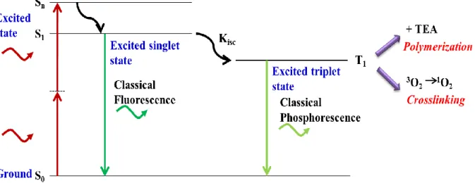
(33) absorption cross-section. p 2 n 2 f p. ( NA) 2 2 c . 2. (2-1). To allow multiple photons absorbed simultaneously, high photon flux densities are required because n-photon absorption cross-section is very small and the probability of n-photon absorption is proportional to the nth power of the photon flux density. Therefore, unlike single photon excitation, MPE can only occur in the focal volume of the laser beam. This unique characteristic of MPA has been applied in multiphoton imaging which attenuates bleaching of fluorophores out of focus and in multiphoton microfabrication as a 3D freeform fabrication technique. Based on above mechanism, multiphoton-induced photochemistry is adopted to fabricate microstructure with monomer resin or proteins. According to different materials, its mechanism can be classified into two different types. One is polymerization for polymer materials, and the other is crosslinking for biological materials such as BSA, FN, and LN. Photosensitizer/photoinitiator is similar to fluorescent dye and is necessary to start the reaction in both photochemistry processes. In our experiments, fluorescent dye of RB is usually used to start the photochemistry. Figure 2-1 shows the Jablonski diagram of RB. Electron of photosensitizer absorbs two photons or multiple photons simultaneously, and jumps from ground state (S0) to its excited state (Sn). The electron quickly decays nonradiatively (~10-12 s) with near unit efficiency to the lowest excited state (S1) by internal. 13.
(34) Figure 2-1 Jablonski diagram of RB with two-photon excitation. conversion. Portion of electrons at the lowest excited state then relax to the ground state and emit fluorescence. For RB, an efficiency of >98% of electrons at lowest excited state can transfer into long-lived (1 ms) triplet state (T1) by intersystem crossing; finally, slight fraction of electrons in the triplet state relax to the ground state and emit phosphorescence. However, electrons at the triplet state can easily cause a chemical reaction. Eq. (2-2) describes the two-photon excited polymerization (TPP) process. Polymerization is a chain reaction and can be distinguished into three important steps: initiation, propagation and termination. The photoinitiator RB absorbs photon energy and is activated into triplet state ([RB]triplet), the formation of a long lived triplet state can initiates a free-radical polymerization mechanism in the presence of a co-initiator (TEA). Finally, the process becomes a chain reaction until the chained radical meets another chained radical.. 14.
(35) RB 2h [ RB ]triplet [ RB ]triplet TEA [ RB ] TEA TEA monomer R . R (monomer) n1 R (monomer). (2-2) n. On the other hand, electrons at the triplet state will also activate the surrounding triplet oxygen (3O2) easily and generate singlet oxygen (1O2) by Förster resonance energy transfer (FRET). Eq. (2-3) describes the reaction of two-photon excited crosslinking (TPC) process. The photosensitizer RB in crosslinking process is also called the photoactivator, which absorbs two photons energy to achieved triplet state, then reacts with triplet oxygen to generate singlet oxygen. Singlet oxygen can oxidize amino acid residues of protein to become an activated protein. Then, an activated protein is crosslinking with the other protein via the covalent bond to form a crosslinked microstructure. RB 2h [ RB ]triplet [ RB ]triplet [O2 ]triplet RB [O2 ]sin glet [O2 ]sin glet protein protein * protein protein [ protein ]crosslinked *. (2-3). *. Using MPE microfabrication has several advantages. First, because polymerization or crosslinking process is confined to only the focal volume of a laser spot, this allows for precise spatial fabrication in solution by avoiding nonspecific polymerization outside of the focal volume. Second, there is reduced photobleaching of the photoactivatable dyes used for polymerization. 15.
(36) or crosslinking. Finally, there is no linear near-IR absorption out of the focal plane in most biomolecule samples. By precise control and move the focusing spot of femtosecond laser, a 3D arbitrary sub-micron microstructure can be fabricated.. 2.3 Sample preparation and neuron culture In order to provide a flat, native and stabile base, a microscope slide must be modified before the protein structures are fabricated on it. First, the glass slides were sonicated in a 1:1000 dilution of detergent (Aldrich Micro 90C) in deionized (DI) water for 15 min and then washed with DI water 15 min for 3 times. The surface was dried with nitrogen or argon; dried in oven for 30min at 120 oC. The plasma cleaner was used for removing the oxide on the surface at 0.3 Torr pressure for 3 min. The slides were then soaked overnight in a solution of 0.5% (v/v) ODTS (n-Octadecyltrichlorosilane, Gelest, Morrisville, PA) within toluene in an inert, moisture-free environment to form a self-assembled organosilane monolayer. After soaking, the slides were washed three times with anhydrous toluene to remove any residual ODTS, dried with nitrogen, and heated for 30 min at 120 °C to complete the formation of the Si-O bond. If need, the silanized slides were immersed in 10 mg/mL solution of BSA (Sigma) to form a monolayer base. The BSA monolayer was used as a non-specific surface compare with the adhesion dynamics of the cells on or off the crosslinked protein structures. In this study, five different fabrication materials were used. First solution. 16.
(37) consisted of Rose Bengal (RB, Sigma-Aldrich, USA) as the photoinitiator incorporated within 0.1 M triethanolamine (TEA) co-initiator (Sigma-Aldrich, USA), and mixed into a 50% (v/v) ethoxylated trimethylolpropane triacrylate (TMPTA) solution. The second one containing Bovine Serum Albumin (BSA, Sigma, St. Louis, MO) and RB as the photoactivator were prepared at the concentrations of 100 mg/mL and 1mM, respectively. Other fabrication solutions consisted of Fibronectin (FN; 1mg/mL, Millipore, Billerica, MA) or Laminin (LN; 1mg/mL, Millipore, purified from mouse) mixed with 1 mM RB. The last one is gelatin (Sigma-Aldrich, USA) mixed with 1 mM RB. If needed, the slides will be coated with PDL or PLL for 30 min at room temperature and rinsed with DI water three times at first. All of the solutions were confined in a small circular rubber chamber (Grace Bio Labs, SA8R-0.5) for fabrication. After fabrication, the structures were rinsed with PBS pH 7.4, and then kept hydrated for cell plating. Neurons used in this study were E18 rat cortical neurons and E15.5 mouse cortical neurons. Cells were isolated and cultured according to established methods [65]. Briefly, the day before the dissection prepare the plating medium (PM) and serum-free medium (SFM) and put them into 37 °C, 5% CO2 incubator. PM consists of neurobasal medium, B27 supplement, 2 mM glutamine, 0.3% glucose, 37.5 mM NaCl and 5% fetal bovine serum (FBS). SFM is the same as PM but without FBS. Neurons were dissociated by treating with trypsin (0.25%, 20 min, 37 °C), triturated with a micropipette tip several times, spin in the centrifuge with 350rpm for 7 minutes and diluted in. 17.
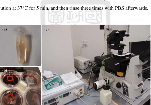
(38) PM. Cells were plated onto fabricated substrates at a density of 80000 cells/mL. One hour later, the sample is flooded with 3mL warmed, CO2-equilibrated SFM and incubated for 3 to 5 days. Time-lapse images were acquired on an inverted microscope (Nikon ECLIPSE Ti) equipped with a CCD camera (QIMAGING RETIGA 2000R) and an automatic temperature, CO2, and humidity controller (Pathology Devices, Inc. LiveCell Controller). The samples were maintained at 37°C and phase contrast images were acquired with 10x or 20x objective at 15 min intervals for a total period of 3 to 5 days. If needed, neurons were fixed with 4% paraformaldehyde (PFA) solution at 37°C for 5 min, and then rinse three times with PBS afterwards.. (a). (c). (b). Figure 2-2 (a) Primary rat/mouse cortical neurons; (b) sample preparation for cell culture; (c) time-lapse microscope with an automatic temperature, CO2, and humidity controller.. 18.
(39) 2.4 Experimental setup and results 2.4.1 Optical setup and instrument control The multiphoton fabrication instrument which was used in this chapter is shown in Fig. 2-3 [66]. In brief, a ti:sapphire laser is coupled to a upright microscope stand (Axioskop 2, Zeiss, Thornewood, NY) and scanning is performed through a combination of laser scanning galvos (Cambridge Technolgoies, Bedford, MA) and a motorized stage (x-y-z, Ludl Electronic Products Ltd, Hawthorne, NY)) under LabVIEW control with a field programmable gate array (FPGA) board (Virtex-II PCI-7831R, National Instruments, Austin, TX). The laser power is controlled through a 10 kHz EOM (Conoptics, Danbuty, CT) and the laser is rapidly shuttered by the other higher speed EOM (maximum 100 MHz, Conoptics). Refractive elements such as objective and lenses can induce additional group velocity dispersion into the overall system. To correct this issue, the prism pair was adjusted to approach the optimal pulse width (< 120 fs). The objectives used for this study are 10x 0.5 NA or 20x 0.75 NA, and the largest fabrication area are 800 μm × 800 μm and 400 μm × 400 μm respectively. Parameters such as power, scanning area, the scan rate of galvos, the repetition of scanning pattern (#scans/layer) are set within the graphical user interface (GUI). There are four First-In First-Out (FIFO) channels in communications between the CPU and FPGA. The first two FIFO channels relay information from the main LabVIEW program to the FPGA to control the galvo mirrors and fast EOM shutter, while the other two record information from the PMT to create a live image of the fabrication 19.
(40) making the communication between CPU and hardware near real-time.. 2.4.2 Neuronal growth on 2D micropatterns In the 2D experiments, two kinds of patterns are designed for the studies of neural guidance behavior, which are line pattern with different periodicity and the positive & negative patterns. The concept of positive pattern means the area which we fabricated is utilized to guide axonal outgrowth; in contrast, negative pattern represents the region created is used for restriction of neurite growth. Figure 2-4 shows the neurons cultured on FN fibers at different time state with periodicity of 10 μm and line width of 1 μm. Based on the results, neurons seems like to extend their axons along the FN fibers; however, it is. Figure 2-3 Optical configuration of the fabrication system, incorporating separate EOMs for power control and rapid shuttering and an FPGA for control of the fabrication process [66].. 20.
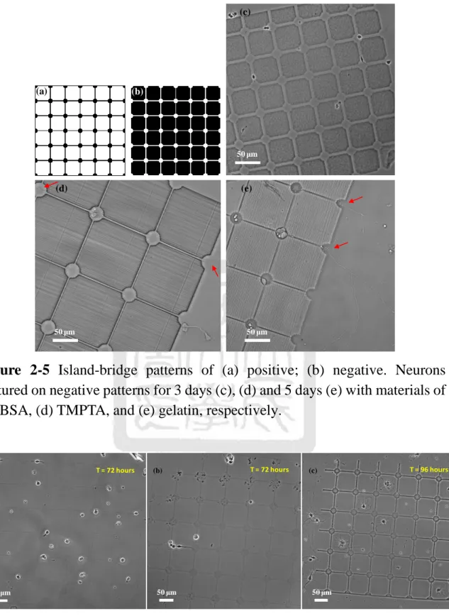
(41) interesting that somas also moved along the fibers back and forth especially when there are other neurons around them. Once finding other neurons, they will migrate toward them and regardless of these fibers. Hence, the results implied that neuron-neuron interaction is superior to that of neuron and FN. The simple island-bridge patterns shown in Figs. 2-5(a) and 2-5(b) were used to realize the concept of positive and negative pattern where black area is the position that will be fabricated. The diameter of the island is around 30 μm and the bridge width varies from 3 μm to 8 μm. The materials used for negative pattern should be something which neurons don’t like; as the result, BSA, TMPTA and gelatin were chosen for this purpose. The slides were coated with PLL/PDL for 30 min at first as an attachment factor which improves neurons adherence, and then fabricated 2D negative patterns on this PLL/PDL monolayer via MPE photochemistry. We got the pretty good results of these negative patterns, which somas of neuron can be constrained on the islands and only extended the axons along the bridge for dozens or hundred of microns to reach other axons or neurons. However, if the width of bridge is large enough (> 5 μm), sometimes neurons will squeeze themselves and go through the bridge as well. Figures 2-5(c), 2-5(d), and 2-5(e) are the phase contrast images of the negative patterns using BSA, TMPTA and gelatin, respectively, and the images were acquired after 3 and 5 days culture.. 21.
(42) (a). (b). 50 μm. 50 μm. (c). (d). 50 μm. 50 μm. Figure 2-4 Rat cortical neurons cultured on FN fibers with line width of 1 μm and periodicity of 10 μm at different time state. (a) t=9 hours; (b) t=15 hours; (c) t=27 hours, and (d) t=36 hours.. In the beginning, we thought ECM proteins should be considered as attractive cues for guidance of axonal growth. Therefore, FN and LN were utilized as the fabrication materials for positive pattern. However, the results indicated most of axons didn’t care about the LN or FN positive patterns very much, only few axons can grow along the bridges; nevertheless, the length of extended axons were only dozens of microns for 2 or 3 days culture as shown in Fig. 2-6(a). One of the possible hypothesis why neurons didn’t respond to positive pattern might be the concentration of LN/FN is too high; therefore, interaction between 22.
(43) (c). (a). (b). 50 μm. 50(d) μm. (e). 50 μm. 50 μm. Figure 2-5 Island-bridge patterns of (a) positive; (b) negative. Neurons cultured on negative patterns for 3 days (c), (d) and 5 days (e) with materials of (c) BSA, (d) TMPTA, and (e) gelatin, respectively.. (a). 50 μm. T = 72 hours. T = 72 hours. (b). 50 μm. (c). T = 96 hours. 50 μm 50 μm. Figure 2-6 Positive island-bridge pattern of (a) FN with concentration of 1 mg/ml; (b) FN/BSA mixture with concentration of 500 μg/ml and 100 mg/ml, respectively; (c) LN/BSA mixture with concentration of 50 μg/ml and 100 mg/ml, respectively.. 23.
(44) integrin receptor and ECM protein is saturated, and neurons can not sense the protein anymore. To deal with this issue, we fabricated the positive pattern with BSA as a backbone and mixed with low concentration of LN or FN (500 μg/ml and 50 μg/ml). The results of 500 μg/ml were almost the same as previous 1 mg/ml one; namely neurons didn’t respond to the patterns so much. However, for 50 μg/ml, it might because the dislike of BSA is more than attraction of such low LN concentration, therefore the patterns looked like negative patterns instead, and neurons started to prevent themselves from contacting the patterns. Hence, based on the above experiments, we got a conclusion that maybe the primary rat/mouse cortical neurons we used here are not very sensitive to the FN or LN which we have. On the other hand, the other approach for creation of PDL/PLL positive patterns has also been developed at the same time. This method consists of three main steps; namely, using MPE to fabricate TMPTA mask on the slide at first, then coating the sample with PDL/PLL for 30 min and rinsing with DI water three times. Finally, the TMPTA masks were removed via sonication. The PLL used for this experiment is labeled with FITC dye (excitation: 494 nm ; emission: 518 nm), therefore it is very easy to examine if axons grow along the PLL positive patterns via fluorescence images. Figure 2-7(a) shows the phase contrast image of cortical neurons grew on PLL positive patterns for 36 hours, and Fig. 2-7(b) is the corresponding fluorescence image while the green fluorescence came from FITC or RB. Square patterns shown in the figures are some TMPTA masks that were still not removed from the slide.. 24.
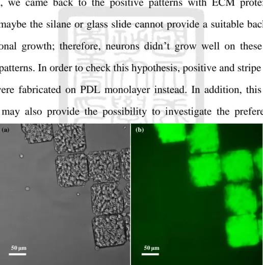
(45) However, if sonicating the sample for longer time, all of the masks can be peeled off clearly. The results indicated that somas of neuron can attach on the island and extend their axons along the bridge for few hundred microns. Figure 2-8(a) is the superimposition of phase contrast image and fluorescence image of neurons which were cultured on samples for 72 hours, and Fig. 2-8(b) is the phase contrast image for 108 hours of culture, respectively. It is very successful that axons formed a well-organized network that we designed for them. Then, we came back to the positive patterns with ECM proteins, and thought maybe the silane or glass slide cannot provide a suitable background for neuronal growth; therefore, neurons didn’t grow well on these LN/FN positive patterns. In order to check this hypothesis, positive and stripe patterns of LN were fabricated on PDL monolayer instead. In addition, this kind of samples may also provide the possibility to investigate the preferences of (a). (b). 50 μm. 50 μm. Figure 2-7 (a) Phase contrast image of rat cortical neurons after 36 hours of culture on PLL positive patterns. (b) Corresponding fluorescence image at the same position as (a).. 25.
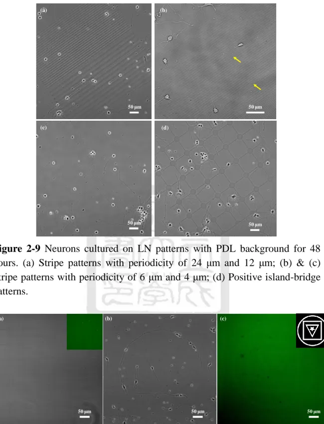
(46) (a). (b). 50 μm. 50 μm. Figure 2-8 (a) Combination of phase contrast image and fluorescence image of neurons which were cultured on FITC-PLL positive patterns for 72 hours. (b) Phase contrast image of neural network after 108 hours culture on PLL positive patterns. neuronal growth between charge interaction and integrin interaction. Figures 2-9(a), 2-9(b), 2-9(c), and 2-9(d) show the results that neurons cultured on stripe patterns with periodicity of 24 μm, 12 μm, 6 μm, 4 μm, and positive island-bridge patterns, respectively. Surprisingly, for large periodicity (i.e. 24 & 12 μm), neurons liked to attach on PDL background much more than on LN stripes, and extend the axons parallel to the stripes for hundred microns. However, if the periodicity is small (i.e. 6 & 4 μm), most of time axons still grew on PDL background and followed the stripes very well, but sometimes they also extended the axons perpendicular to the stripes as shown in Fig. 2-9(c). Therefore, axonal orientation can be strongly guided by changing the periodicity of micro-lines. Lines of larger periodicity reliably produced parallel axonal outgrowth, while lines of smaller periodicity induced perpendicular outgrowth. Moreover, we found out the cell bodies had several. 26.
(47) cytoplasmic extensions and multipolar phenotype were observed on lines with smaller periodicity; however, on larger periodicity of lines most of the neurones were unipolar. Hence, we proposed that larger periodicity induced axonal outgrowth and inhibited dendritic development, whereas smaller periodicity permitted both axonal and dendritic growth. For positive patterns, the results are contrary to our original expectation; axons grew everywhere on PDL background but not on LN patterns. However, when using antibody stain to check the quality of LN patterns on PDL monolayer, we found the fluorescence intensity from the PDL background is higher than that from LN patterns. This situation is not well understood so far. One possible guess now is when doing MPE microfabrication, somehow the PDL monolayer also be damaged by fs laser beam simultaneously, and we called it “MPE etching”. Based on this discovery, the method of creation PDL/PLL positive patterns via MPE etching has also been developed. Compare to the previous method, it is more straightforward and more efficient without creating the mask in advance. Again, the FITC-PLL was utilized to coat the slide at first since it is the easiest way to examine the fabricated results via fluorescence image after doing MPE etching. Figure 2-10(a) is the phase contrast images of patterned FITC-PLL monolayer, although the contrast is not very clearly, one can still see the outline of the patterns, and the relative brighter areas shown in the figure are the positions where we did laser direct etching. Neuron cultured on the other freeform FITC-PLL pattern for 5 days is shown in Figs. 2-10(b), and 2-10(c) is the corresponding fluorescence image at the same spot.. 27.
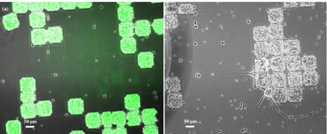
(48) (a). (b). 50 μm. 50 μm. (c). (d). 50 μm. 50 μm. Figure 2-9 Neurons cultured on LN patterns with PDL background for 48 hours. (a) Stripe patterns with periodicity of 24 μm and 12 μm; (b) & (c) Stripe patterns with periodicity of 6 μm and 4 μm; (d) Positive island-bridge patterns. (a). (b). (c). 50 μm. 50 μm. 50 μm. Figure 2-10 (a) Phase contrast images of patterned FITC-PLL monolayer via MPE etching. Inset: corresponding fluorescence images. (b) Mouse cortical neurons cultured on 2D freeform pattern for 120 hours. (c) Corresponding fluorescence images of (b). Inset: designed pattern for etching.. 28.
(49) It is worth mentioning that axonal outgrowth was strongly guided via the designed micropatterns. In addition, we also used this method to etch the LN monolayer. The procedure for coating a LN monolayer is diluting LN solution into the concentration of 50 μg/ml at first, then coat slide surface with a minimal volume, incubate at 37 °C for half hour, wash the slide 3 times with PBS finally. As mentioned above, in order to check the quality of patterned LN monolayer after laser direct etching, we used the antibody stains for LN and the results are demonstrated in Fig. 2-11. Based on these clear stained images, we believed this method is also suitable for etching of other proteins and materials; namely, not only for LN but may hold potential for many other applications in the future. The ovarian cancer cells were cultured on this kind of LN patterns at first since cancer cells always grow faster and much easier to culture. The results showed that cells can sense the LN protein and respond to it very quick as shown in Fig. 2-12. However, when we came back to neurons, they just grew randomly on LN patterns and didn’t care much about LN at all. This results double confirmed our previous conclusion that the primary cortical neurons we used here are not sensitive to LN which we have. In the end, the other protein called “L1” has also been used for the study of axonal guidance. The regular procedure for preparation of L1 monolayer is coating the surface with PDL/PLL for 30 min at first, then coating L1 protein with the concentration of 50 μg/ml for 15 min, and finally washing the sample with DI water 2 times. The method of MPE etching was used again to create the. 29.
(50) patterned L1+PDL layer. The results are shown in Fig. 2-13, and we can see again that axons grew along the positive patterns very well which we designed for them as the previous PLL/PDL positive patterns. As a result, we concluded that besides PDL and PLL, L1 protein can also be considered as a suitable material for guidance of axonal outgrowth of cortical neurons. Based on above method, distance dependence of neuronal outgrowth on patterned L1+PDL surface has been studied. The principle is to pattern both cytophilic (cell-attractive) and cytophobic (cell-repulsive) chemical and geometrical cues on the same surface and to use these patterns to confine both the position of the soma and the elongation of the neuritis. For this experiment, the positive island-bridge patterns with gaps of 10, 20, 30, and 50 μm were designed. According to our preliminary results shown in Fig. 2-14, it seems like if the gaps between two bridges are smaller than 20 μm, axons can overcome this barrier and cross the gaps. However, if the gaps are larger than 30 μm, most of axons were constrained on the islands and cannot go through the gaps.. 30.
(51) 100 μm. 100 μm. Figure 2-11 Fluorescence images of large-scale antibody stained LN monolayer with designed pattern which was etched by MPE photochemistry.. (a). 50 μm. 50 μm. 50 μm. 50 μm. (b). (c). Figure 2-12 Phase contrast images of ovarian cancer cells which were cultured on LN monolayer for 24 hours with the patterns of (a) “Nature” words, (b) stripes with periodicity of 12 & 24 μm, and (c) positive island-bridge. Inset: corresponding designed patterns for etching.. 31.
(52) (a). (b). 50 μm. 50 μm. Figure 2-13 Cortical neurons cultured on patterned L1+PDL surfaces for 120 hours which were fabricated by MPE etching.. (a). (b). 20 μm gap. 50 μm gap 30 μm gap. 10 μm gap. 50 μm. 50 μm. Figure 2-14 Phase contrast images of neurons cultured on positive island-bridge patterns of L1+PDL for 120 hours with gaps of (a) 10 μm and 20 μm; (b) 30 μm and 50 μm.. 32.
(53) 2.4.3 3D microstructures for axonal guidance So far, we made a lot of efforts on 2D micropatterns for neuronal guidance, therefore, didn’t explore so much about 3D stuffs. All we focus now are few simple microstructures which can restrict or guide axonal outgrowth in 3D microenvironments. As we know, current high-throughput screening of cell function and in vitro cell–cell communication studies requires routine generation of large-scale single-cell arrays with high precision and efficiency. This is also true for neuronal studies and our method of MPE fabrication also can match all of these requirements. As a result, the first structure we designed for this purpose is 3D microhole and microchannel arrays, which were utilized to constrain single-neuron in single hole and only extend their axons along the designed 3D channels as illustrated in Figs. 2-15(a) and 2-15(b). The materials used for this experiment could be one of BSA, TMPTA or gelatin. However, gelatin is the best candidate since it is more biocompatible than TMPTA and can be fabricated as fast as TMPTA. Figure 2-16 is shown that single neuron can actually be constrained in single hole and extend the axon along the microchannel longer than 600 μm for 72 hours of culture. Nevertheless, the seeding density of neurons now is only about 40~50% and needed further improvement to increase this percentage, such as increasing cell density or modifying the microstructures. In many of our previous patterning experiments, when two axons approach one another along intersecting orthogonal paths, the process that crosses the intersection first dominates the growth of the second. In most. 33.
(54) Figure 2-15 (a) Top view, and (b) bottom view of 3D microchannel structures with hole diameter of 15 μm, channel width of 5 μm, and height of 25 μm. (c) Scheme of 3D microgroove-bridge structures with groove width of 12 μm, and height of 20 μm.. cases the second process fasciculate with the first instead of following its initial path. Even in the limited cases where the second process crosses the first, they still interact with one another through membrane contact. Ideally to form complex neural networks, we would like to form process crossings that do not interact with one another. To do so we tried to construct 3D ‘axon bridges’ that allow processes to grow underneath and over the top of the bridge, while being isolated from one another. Figure 2-15(c) illustrates the designed 3D microgroove & microbridge structures which were used to realize this idea. In the beginning, we also used gelatin as the material for this structure. However, the results shown in Fig. 2-17(a) indicate that neurons can stay in the groove and extend their axons along the groove for a long distance, but almost no neurons attached on the bridge yet. The reason for this might because neurons liked to attach on PDL background much more than on gelatin surface. To solve this problem, we mixed gelatin solution with PDL at. 34.
(55) the ratio of 1:1, and then used this mixture to fabricate the structures again. The results came out very well, and were demonstrated in Figs. 2-17(b) and 2-17(c). The two images were captured at the same x-y position but at different heights. The clear focal plane of 2-17(b) is in the groove, however for 2-17(c) is on top of the bridge, and the height difference between two images is 20 μm. Neurons in the groove can extend the axons underneath the bridge and follow the rail for a long distance. On the other hand, the other neurons can also attach on the surface of bridge and extend the axons to other bridges or targets without disturbing the growth of neurons in the groove. Finally, since the mixture of gelatin and PDL can be fabricated into 3D freeform structures by MPE photochemistry and also provided attachment factors for neuronal outgrowth, we decided to utilize it for creating other samples. The cone shaped structures were designed as illustrated in the inset of Fig. 2-18. Interestingly, axons grew along the outline of the microstructures very well and formed a circular shape as shown in Fig. 2-18. However, it is. Figure 2-16 Phase contrast images of neurons cultured on 3D microchannel arrays with PDL background for 72 hours.. 35.
(56) hard to tell if they grew in 3D or just in plane based on the phase contrast images. Hence, other processes such as transfect or stain should be done for further observation via fluorescence. Nevertheless, we believe if the step size between two planes was decreased or make it become spiral fashion in 3D space, axons definitely will follow the spiral path from the bottom to the top of cone, which is a great evidence that axonal outgrowth can be guided in 3D microenvironment via a well-controlled manner. (a). 50 μm. (b). (c). groove bridge. groove Height difference between bridge two images is 20 μm. 50 μm. 50 μm. Figure 2-17 Phase contrast images of neurons cultured on 3D microstructures of (a) gelatin only for 72 hours; (b) & (c) mixture of gelatin and PDL for 40 hours. All of the structures were fabricated on PDL monolayer.. 36.
(57) Figure 2-18 Phase contrast image of neurons cultured on cone-shaped structures for 72 hours with bottom diameter of 90 μm, top diameter of 10 μm, step size of 3 μm, and height of 20 μm. Inset: Scheme of 3D micro-cone structures.. 37.
(58) Chapter 3 Temporal Focusing-based Fabrication of Polymer Microstructures 3.1 Temporal focusing-based multiphoton excitation In general case, one often uses a lens or objective to focus the collimated light along the propagation direction. The beam spot size will be focused at first, and then diverged along the optical axis; however, the pulse width remains unchanged during the focusing procedure. This is the so called “spatial focusing” as shown in the left hand side of Fig. 3-1. Since a ultrashort laser pulse is composed of different frequency components; therefore, the pulse width can be manipulated if one can control the phase of each frequency component of a pulse. Making all of them in phase on the specific plane, one can get the narrowest pulse width; however, the pulse width will become broader before or after this specific plane and the lateral beam size remains unchanged. This is the concept of temporal focusing which illustrates in the right hand side of Fig. 3-1. The basic principle which was used to realize temporal focusing can be simplified as shown in Fig. 3-2, the key components are a diffraction grating, a collimating lens (focal length of f1) and a high NA objective lens (focal length of f2). Femtosecond pulse derives from the superposition of in phase waves with different wavelengths therefore, when a femtosecond laser pulse incidents onto the diffraction grating, the diffractive. 38.
數據

+7
![Figure 2-3 Optical configuration of the fabrication system, incorporating separate EOMs for power control and rapid shuttering and an FPGA for control of the fabrication process [66]](https://thumb-ap.123doks.com/thumbv2/9libinfo/9235565.496215/40.892.197.680.473.931/figure-optical-configuration-fabrication-incorporating-separate-shuttering-fabrication.webp)

相關文件
電子 、 機械系 、 環工系 、 高分子、光電、電腦與通訊 本學程共計 7 學科, 18 學分,必須修畢全部學分,始
其他光學儀器及設備製造業 從事 2771 細類以外光學儀器及設 備製造之行業,如望遠鏡、顯微
國立高雄師範大學數學教育研究所碩士論文。全國博碩士論文資訊網 全國博碩士論文資訊網 全國博碩士論文資訊網,
結合夥伴協作學校,與大專院校、出版社及電 子學習平台機構組成專業協作社群,以資訊素
電機工程學系暨研究所( EE ) 光電工程學研究所(GIPO) 電信工程學研究所(GICE) 電子工程學研究所(GIEE) 資訊工程學系暨研究所(CS IE )
學博士,現為上海大學文學院教 授,兼任佛光山人間佛教研究院
第二章是介紹 MEMS 加工製程,包括體型微加工、面型微加工、LIGA、微 放電加工(Micro-EDM)、積體電路相容製造技術 CMOS MEMS 製程等。製作微 加速度感測器。本研究是選用台積電 0.35μm
實驗操作與多元學習,使學習者能具備科學核心 知識、探究實作與科學論證溝通能力,並強調跨
