Characteristics of InGaN/sapphire-based photovoltaic devices with
different superlattice absorption layers and buffer layers
Chih-Ciao Yang*
a, Jinn-Kong Sheu
ab, Min-Shun Huang
a, Shang-Ju Tu
a, Feng-Wen Huang
a,
Kuo-Hua Chang
a, Ming-Lun Lee
bcand Wei-Chih Lai
aba
Institute of Electro-Optical Science and Engineering, National Cheng Kung University, Tainan City,
Taiwan 70101
b
Center for Micro/Nano Science and Technology, National Cheng Kung University, Tainan City,
Taiwan 70101
c
Department of Electro-Optical Engineering, Southern Taiwan University, Tainan, Taiwan 71005
ABSTRACT
In this study, hetero-structure p-i-n type epitaxy wafers were deposited on the GaN/sapphire templates with different buffer layers by the MOVPE system. The absorption layers sandwiched in top p-GaN and bottom n+-GaN layers were designed into different short-period InGaN/GaN superlattice structures with specific pair numbers to maintain a total absorption thickness of 200 nm. As the buffer layer was properly adjusted, the VOC and JSC were enhanced by 35% and
95%, respectively. In addition to material qualities, the thickness of GaN buffer layers and piezoelectric-induced stain in the InGaN film itself also influenced the PV device performance.
Keywords: InGaN, GaN, sapphire, photovoltaic, superlattice, buffer layer.
1. BACKGROUND OF NITRIDE-BASED PHOTOVOLTAICS
Bandgap engineering of group III-nitride compound semiconductors between indium nitride (InN, ~ 0.7eV) and gallium nitride (GaN, ~3.4 eV) by the InXGa1-XN alloy system makes it possible for the full-solar-spectrum photovoltaic (PV)
applications since the bandgap energy of InN was confirmed in 2002 [1-2]. Recently, because of the potential multi-junction solar cells for ultra-high conversion efficiency over 50% by optimum bandgaps, aiming at terrestrial power plants (high concentrated PV) and extraterrestrial satellites, many research groups have reported their efforts in the research of the InGaN/sapphire-based PV devices, mainly including multiple quantum well (MQW) [3-5], p-i-n junction [6-9] and short-period superlattice (SPS) designs [10-11]. However, the present InGaN-based materials exhibit more difficulties in the epitaxy growth than conventional Si or GaAs semiconductors. The native structure defects mainly originate from lattice-mismatched substrates. The different lattice constants between GaN and InXGa1-XN could limit the
critical thickness of epitaxial layers, uniformity of indium content, alloy miscibility and other problems in the crystal growth [12]. It is still a great challenge to grow low bandgap InGaN because material qualities degrade rapidly with the increase of indium contents and thickness of InGaN semiconductors. Critical thickness and threading dislocations (TDs) limit the power conversion efficiency (PCE) of PV devices [13-14].
In this study, different InGaN/GaN superlattice structures were applied as the active layers of PV devices. The composition of low-bandgap absorption layers was divided into thin InGaN/GaN (well/barrier) SPS layers to prevent from depositing thick InGaN bulks with high indium contents. In order to clarify how high-density TDs affect the InGaN-based PV devices, the underlying buffer layers were also compared. We shall discuss the x-ray diffraction analyses of materials, and power conversion characteristics of devices from solar irradiance of AM1.5G standard testing conditions. Finally, the energy-band diagrams in the active layers of PV devices are also simulated to help understand the electric fields in the PV devices.
2. EXPERIMENS
2.1 Nitride-based PV structure designs
The InGaN/GaN epitaxy wafers in this study were deposited on c-face sapphire (Al2O3) substrates by a metalorganic
vapor-phase epitaxy (MOVPE) reactor (EMCORE D-180). Figure 1 shows the schematic structures of the PV devices. First, two templates consisting of different thickness of 2- and 4-μm-thick undoped GaN (u-GaN) buffer layers were prepared, respectively. Then, InGaN/GaN p-i-n structure was simultaneously deposited on both the templates with 2- and 4-μm-thick u-GaN, where the samples were labeled as A-2 and A-4, respectively. Samples A-2 and A-4 consisted of a 1-μm Si-doped n+-GaN bottom layer (n~ 5×1018 cm-3), an undoped InGaN/GaN (2 nm/4 nm for 33 pairs) SPS structure, and a 100-nm-thick Mg-doped p-GaN (p~ 5×1017 cm-3) top layer in series. Meanwhile, another main p-i-n structure with a different InGaN/GaN (3 nm/4 nm for 28 pairs) SPS structure was also deposited on both u-GaN templates, and the samples were labeled as B-2 and B-4, respectively. Both the A- and B-series samples have the same active-layer thickness (200 nm) of the InGaN/GaN SPS layers.
Figure 1. The schematic structures of the PV devices of two buffer layer thickness and two compositions of SPS absorption layers.
2.2 Fabrication process
The fabrication process of the PV devices is similar to conventional GaN/sapphire-based light emitting diodes (LEDs) with lateral electrodes. The inductively-coupled plasma (ICP) dry etching is applied to expose the underlying n+-GaN for the formation of Ohmic contacts. Besides, the Ohmic contact for the p-GaN top layer is indium tin oxide (ITO) rather than thin Ni/Au bilayer metal which shows much lower transparency in near ultraviolet regions. Finally, the Cr/Au (50/1000 nm) bilayer metal is deposited onto the exposed n+-GaN surface and the ITO layer at the same time to serve as the cathode and the anode electrode pads, respectively. The active area of each fabricated device is 0.02 cm2 with a 10% electrode coverage-rate. Lateral electrode pads are in digitated arrangement to have better current collection for the insulating sapphire substrate.
3. RESULTS AND DISCUSSION
3.1 X-ray diffraction analyses
Figure 2 shows the (002) x-ray diffraction (XRD) spectra of different p-i-n PV epitaxial wafers. According to the separation of the adjacent diffraction peaks, one could determine the periodic structures that the thickness of a single pair InGaN in samples A-2 and A-4 were 2 nm, and in samples B-2 and B-4 were 3 nm, respectively; the indium contents in the well layers of samples A-2 and A-4 were 24% and 22%, and those of samples B-2 and B-4 were 24% and 23%, respectively. As shown in the inset of figure 1, the enlargement indicated a little blue-shift when the main structures were grown on thicker u-GaN templates. It could be attributed that lattice constants of epitaxial layers were more relaxed on the thicker u-GaN template layers [15]. On the other hand, the zeroth-order diffraction peaks of the InGaN/GaN signals both showed a decreased full-width-half-maximum (FWHM) for samples A-4 and B-4, as compared with those of samples A-2 and B-2.
Figure 2. The (002) XRD patterns of different p-i-n PV epitaxial wafers. The inset shows the enlargement of the zeroth-order diffraction peaks.
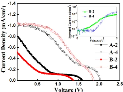
3.2 AM1.5G solar response
Figure 3 shows the relationship of current density and voltage (J-V) for the PV devices measured by the solar simulator (model: Oriel M-91190A), calibrated by the calibration cell from NREL of global air-mass 1.5 (AM1.5G) standard testing conditions. The measured PV parameters are summarized in Table 1. As the thickness of underlying u-GaN buffer layers was increased, the PV devices showed enhanced open-circuit voltage (VOC) in devices A-4 and B-4, as
compared with devices A-2 and B-2, respectively. The increased VOC could be attributed to the fewer leakage paths in
the devices with 4-μm-thick u-GaN buffer layers that the TD density in GaN/sapphire epitaxial layers becomes lower when the thickness of the buffer layer is increased [16]. However, the TD-related defects are usually charged. As shown in the inset of figure 3, the recombination current of device B-2 at low bias is much larger than that of device B-4. From a simple solar cell circuit model, the VOC value is logarithmically proportional to the reciprocal of the reverse saturation
current, which represents the recombination current in the quasi-neutral regions. The decreased TD density could potentially reduce the saturation current and therefore increase VOC values [17]. Besides, the solar response of each SPS
PV device shows non-typical J-V curves that the fill factor (FF) is quite low. This could be attributed to the recombination in the space charge region of InGaN/GaN SPS layers with densely charge-related defects [18]. When the buffer layer thickness of u-GaN is increased to 4 μm, PV devices (sample A-4 and B-4) shows much higher FF as compared to 2-μm-thick u-GaN buffer layers (sample A-2 and B-2). On the other hand as shown in figure 3, PV devices exhibited large series resistance (RS), which degrades the PCE, mainly resulting from the 200-nm-thick i-layer of
InGaN/GaN SPS structures. This phenomenon leads to a low FF and reduced photocurrent values of the PV devices. In principle, the electron wavefunction is more coupled between adjacent wells by thicker InGaN of the sample B-4 than in thinner InGaN wells of sample A-4. This is due to the fact that polarization field and the quantity of bandgap narrowing increase with the increase of the strained layer thickness. Theoretically, device B-4 should have larger short-current density (JSC) than device A-4 as a consequence of the effectively lower bandgap energy in the active region of
InGaN/GaN SPS structures. However, the dilemma comes from the material qualities that degrade dramatically as the InGaN thickness increases so that limit the device performance far from the theoretical values.
Table 1. Measured PV parameters of each fabricated device by AM1.5G illumination.
Sample VOC (V) JSC (mA/cm 2 ) FF PCE (%) A-2 1.60 0.83 0.13 0.18 A-4 2.04 1.01 0.32 0.66 B-2 1.38 0.53 0.16 0.11 B-4 1.86 1.03 0.43 0.82
Figure 3. Typical J-V characteristics of PV devices illuminated under AM1.5G standard testing conditions. The inset shows the recombination current biased at low forward voltage.
4. ENERGY-BAND DIAGRAM SIMULATION
4.1 Introduction
A number of quantum-well material systems are in the research and applied to PV applications, such as strain-balanced GaAsP/InGaAs, lattice-mismatched GaAs/InGaAs, GaAsP/InGaAs and InP/InAsP, lattice-matched InP/InGaAs and AlGaAs/GaAs systems, and GaInNAs/GaAs superlattices [19-21]. The quantum-well PV devices could improve the long-wavelength response and current density in short absorption layer thickness. When we study a single quantum well of a hetero-structure, the electron wavefunction was found to have finite probability to penetrate into the barrier layers. If the potential well/barrier layers alternate and the period number is large enough, the periodic system could be considered as an artificially one-dimensional lattice [22]. When the wavefunction of each isolated single-quantum-well is coupled through tunneling effects, each energy level of an isolated quantum well becomes an energy band to form a superlattice. However, the theory of a real superlattice is not simple because of complex by inter-diffusion and different effective-masses in the well and the barrier layers.
In this study, the superlattice structure was applied to the active layers of PV devices. The composition of the low-bandgap absorption layer was divided into thin InGaN/GaN layers to prevent from depositing thick InGaN bulks with high indium contents. Based on the same indium content, the PV deices with the InXGa1-XN/GaN superlattice rather than
a thick InXGa1-XN single layer have been demonstrated to show better optical and electrical properties [10]. The stacked
superlattice structure in thin barrier and well layers is realized instead of thick InGaN layers with high indium compositions that easily induce poor material qualities. Besides, the superlattice design could allow more coupled wavefunctions than the MQW design that photogenerated carriers are more localized in the well layer of the MQW structure.
4.2 Simulation setup
The energy-band diagrams of InGaN/GaN heterostructures were simulated by the software tool SiLENSe [23]. For comparison, the InGaN/GaN SPS PV structures were simplified to begin at an n+-GaN (n=5×1018 cm-3; 100 nm) layer, an InGaN/GaN SPS structure (background concentration=1×1016 cm-3) and a p-GaN (n=5×1017 cm-3; 100 nm) layer where the indium content of InXGa1-XN well layers was set as 24%. The Thickness of two InGaN/GaN SPS structures was 2
nm/4 nm (33 pairs) and 3 nm/4 nm (28 pairs), respectively, to both have the total absorption thickness of around 200 nm.
4.3 Simulation results
Figure 4 shows the simulated energy-band diagrams of InGaN/GaN (2 nm/4 nm) under forward bias at 0, 1 and 2 V, respectively. Noteworthily, the trend of built-in electric fields in the InGaN/GaN SPS layer was unfavorable for the photogenerated carriers of a PV device and became worse as the forward bias increased. This was consistent in the
experiment results of AM1.5G solar response of the SPS-type PV devices that the photocurrent degraded as the voltage increased. This was attributed to the spontaneous and piezoelectric polarization caused by the InGaN layers in the SPS structures [24]. Namely, the opposite trend increased with the increase of indium contents in the SPS layer and the increased thickness of InGaN well layers. As shown in figure 5, the opposite trend of built-in electric fieldsbecame higher while the thickness of In0.24Ga0.76N well layers was increased from 2 nm to 3 nm.
Figure 4. Simulated energy-band diagrams of InGaN/GaN (2 nm/4 nm) under forward bias at 0, 1 and 2 V.
Figure 5. Simulated energy-band diagrams of PV devices with different thickness of In0.24Ga0.76N/GaN SPS
structures at zero bias.
5. CONCLUSION
The underlying u-GaN buffer layer thickness was increased to grow main InGaN-based PV devices. The JSC of devices
A-4 and B-4 were enhanced by 22% and 94%, as compared with that in devices A-2 and B-2, respectively. This is because the probability of scattering is decreased in the active regions with lower TD density, and hence photogenerated carriers could transport more easily to reach the external circuits. Device B-4 with a better coupled wavefunction in the
superlattice active-region yielded the AM1.5G power conversion efficiency of 0.82%, mainly limited by the epitaxy technology so far. It is necessary to improve the material qualities to lower down the TD density and reduce the RS of
InGaN materials before the full-solar-spectrum InGaN-based PV devices are realized.
When the indium content of InXGa1-XN is increased to absorb more sunlight, the polarization effects of InGaN layers in
SPS structures must take into consideration. Although the opposite trend of built-in electric fields caused by the polarization of InGaN layers could be decreased by increasing the thickness of GaN barrier layers or aluminum-containing barrier layers (e.g. AlGaN), the localization of photogenerated carriers in the well layers could be a main problem for SPS or MQW InGaN PV designs.
ACKNOWLEDGE
The authors would like to acknowledge the National Science Council for the financial support and provision of the research grant NSC 97-2221-E-006-242-MY3 and the Bureau of Energy, Ministry of Economic Affairs under Contract No. 99-D0204-6. We would like to acknowledge Prof. R. H. Horng for the kindly assistance of simulation.
REFERENCES
[1] V. Y. Davydov, A. A. Klochikhin, R. P. Seisyan, V. V. Emtsev, S. V. Ivanov, F. Bechstedt, J. Furthmuller, H. Harima, A. V. Mudryi, J. Aderhold, O. Semchinova, and J. Graul, “Absorption and Emission of Hexagonal InN. Evidence of Narrow Fundamental Band Gap,” Phys. Status Solidi B 229(3), R1-R3 (2002).
[2] J. Wu, W. Walukiewicz, K. M. Yu, J. W. Ager III, E. E. Haller, Hai Lu, William J. Schaff, Yoshiki Saito, and Yasushi Nanishi, “Unusual properties of the fundamental band gap of InN,” Appl. Phys. Lett. 80(21), 3967-3969 (2002).
[3] O. Jani, C. Honsberg, A. Asghar, D. Nicol, I. Ferguson, A. Doolittle and S. Kurtz, “Characterization and analysis of InGaN photovoltaic devices,” Proc. the 31st IEEE PVSC, 37–42 (2005).
[4] R. Dahal, B. Pantha, J. Li, J. Y. Lin and H. X. Jiang, “InGaN/GaN multiple quantum well solar cells with long operating wavelengths,” Appl. Phys. Lett. 94(6), 063505 (2009).
[5] R. Dahal, J. Li, J. Y. Lin and H. X. Jiang, “InGaN/GaN multiple quantum well concentrator solar cells,” Appl. Phys. Lett. 97(7), 073115 (2010).
[6] O. Jani, I. Ferguson, C. Honsberg and S. Kurtz, “Design and characterization of GaN/InGaN solar cells,” Appl. Phys. Lett. 91(13), 132117 (2007).
[7] C. J. Neufeld, N. G. Toledo, S. C. Cruz, M. Iza, S. P. DenBaars and U. K. Mishra, “High quantum efficiency InGaN/GaN solar cells with 2.95 eV band gap ,” Appl. Phys. Lett. 93(14), 143502 (2008).
[8] R. H. Horng, S. T. Lin, Y. L. Tsai, M. T. Chu, W. Y. Liao, M. H. Wu, R. M. Lin and Y. C. Lu, ”Improved conversion efficiency of GaN/InGaN thin-film solar cells,” IEEE Electron Device Lett. 30(7), 724-726 (2009). [9] R. H. Horng, M. T. Chu, H. R. Chen, W. Y. Liao, M. H. Wu, K. F. Chen and D. S. Wuu, “Improved conversion
efficiency of textured InGaN solar cells with interdigitated imbedded electrodes,” IEEE Electron Device Lett. 31(6), 585-587 (2010).
[10] J. K. Sheu, C. C. Yang, S. J. Tu, K. H. Chang, M. L. Lee, W. C. Lai and L. C. Peng, “Demonstration of GaN-based solar cells with GaN/InGaN superlattice absorption layers,” IEEE Electron Device Lett. 30(3), 225-227 (2009). [11] C. C. Yang, J. K. Sheu, X. W. Liang, M. S. Huang, M. L. Lee, K. H. Chang, S. J. Tu, F. W. Huang, and W. C. Lai,
“Enhancement of the conversion efficiency of GaN-based photovoltaic devices with AlGaN/InGaN absorption layers,” Appl. Phys. Lett. 97(2), 021113 (2010).
[12] S. Nakamura, “The Roles of Structural Imperfections in InGaN-Based Blue Light-Emitting Diodes and Laser Diodes,” Science 281(5379), 956-961 (1998).
[13] N. G. Weimann, L. F. Eastman, D. Doppalapudi, H. M. Ng, and T. D. Moustakas, “Scattering of electrons at threading dislocations in GaN,” J. Appl. Phys. 83(7), 3656-3659 (1998).
[14] M. J. Reed, N. A. El-Masry, C. A. Parker, J. C. Roberts and S. M. Bedair, “Critical layer thickness determination of GaN/InGaN/GaN double heterostructures,” Appl. Phys. Lett. 77(25), 4121-4123 (2000).
[15] K. Kusakabe, A. Kikuchi and K. Kishino, “Characterization of Overgrown GaN Layers on Nano-Columns Grown by RF-Molecular Beam Epitaxy,” Jpn. J. Appl. Phys. 40(3A), L192-L194 (2001).
[16] J. K. Sheu, M. L. Lee and W. C. Lai, “Effect of low-temperature-grown GaN cap layer on reduced leakage current of GaN Schottky diodes,” Appl. Phys. Lett. 86(5), 052103 (2005).
[17] A. Luque and S. Hegedus, [Handbook of Photovoltaic Science and Engineering], John Wiley & Sons Ltd., England, 92-98 (2003).
[18] J. Reichman, “The current-voltage characteristics of semiconductor-electrolyte junction photovoltaic cells,” Appl. Phys. Lett. 36(7), 574-577 (1980).
[19] N. J. Ekins-Daukes, K. W. J. Barnham, J. P. Connolly, J. S. Roberts, J. C. Clark, G. Hill and M. Mazzer, “Strain-balanced GaAsP/InGaAs quantum well solar cells,” Appl. Phys. Lett. 75(26), 4195-4197 (1999).
[20] J. Wu, W. Walukiewicz, K. M. Yu, W. Shan, J. W. Ager III, E. E. Haller, Hai Lu and William J. Schaff, “Superior radiation resistance of In1–xGaxN alloys: Full-solar-spectrum photovoltaic material system,” J. Appl. Phys. 94(10),
6477-6482 (2003).
[21] C.W. Tu, “III-N-V low-bandgap nitrides and their device applications,” J. Phys.: Condens. Matter 13(32), 7169– 7182 (2001).
[22] V. V. Mitin, V. A. Kochelap and M. A. Stroscio, [Quantum Heterostructures], Cambridge University Press, UK, 73-104 (1999).
[23] www.str-soft.com/products/SiLENSe/
[24] V. Fiorentini, F. Bernardini and O. Ambacher, “Evidence for nonlinear macroscopic polarization in III–V nitride alloy heterostructures,” Appl. Phys. Lett. 80(7), 1204 (2002).