It may not be copied or distributed.
may result in severe civil and criminal penalties.
Unauthorized reproduction or distribution of this eBook
Embedded Controller Hardware Design
by Ken Arnold
www.LLH-Publishing.com
www.EmbeddedControllerHardwareDesign.com
any form or means whatsoever, without written permission of the publisher. While every precaution has been taken in the preparation of this book, the publisher and author assume no responsibility for errors or omissions. Neither is any liability assumed for damages resulting from the use of information contained herein.
Printed in the United States of America.
ISBN 1-878707-87-6 (LLH eBook)
LLH Technology Publishing and HighText Publications are trademarks of Lewis Lewis & Helms LLC, 3578 Old Rail Road, Eagle Rock, VA, 24085
Dedication
This book is dedicated in memory of my father, Kenneth Owen Arnold, who always encouraged me to follow my dreams. When other adults discouraged me from entering the engineering field, he told me, “If you really like what you’re doing and you’re good at it, you will be successful.”
Nowadays I get paid to have fun doing things I’d do for free anyway, so that meets my definition of success! Thanks, Dad.
Acknowledgment
This book is a direct result of contributions from many of the students I have been fortunate enough to have in my embedded computer engineering courses at the University of California—San Diego extension. They have provided a valuable form of feedback by sharing their notes and pointing out weaknesses in the text and in-class presentations. Some sections of this text were also provided by David Fern and Steven Tietsworth.
I would also like to thank my family for supporting me and, Mary, Nikki, Kenny, Daniel, Amy, and Annie for being patient and helping out when I needed it!
Table of Contents
Preface ix
Chapter One Review of Electronics Fundamentals...1
Objectives...2
Embedded Microcomputer Applications...2
Microcomputer and Microcontroller Architectures...4
Digital Hardware Concepts...6
Logic Symbols...17
Timing Diagrams...19
Multiplexed Bus...20
Loading and Noise Margin Analysis...21
The Design and Development Process...21
Chapter One Problems...22
Chapter Two Microcontroller Concepts...23
Organization: von Neumann vs. Harvard...24
Microprocessor/Microcontroller Basics...24
The 8051 Family Microcontroller Processor Architecture...27
The 8051 Family Microcontroller Instruction Set Summary...42
Chapter Two Problems...56
Chapter Three Worst-Case Timing, Loading, Analysis, and Design...57
Timing Diagram Notation Conventions...58
Fan-Out and Loading Analysis—DC and AC...63
Logic Family IC Characteristics and Interfacing...75
Design Example: Noise Margin Analysis Spreadsheet...82
Worst-Case Timing Analysis Example...90
Chapter Three Review Problems...92 Click the page number to go to that page.
Chapter Four Memory Technologies and Interfacing...95
Memory Taxonomy...96
Read/Write Memories...100
Read-Only Memory...101
Other Memory Types...104
JEDEC Memory Pin-Outs...105
Device Programmers...106
Memory Organization Considerations...107
Parametric Considerations...109
Asynchronous vs. Synchronous Memory...110
Error Detection and Correction...111
Memory Management...113
Chapter Four Problems...115
Chapter Five CPU Bus Interface and Timing...,....117
Read and Write Operations...,...117
Address, Data, and Control Buses...,...118
Address Spaces and Decoding...,...120
Chapter Five Problems...,...124
Chapter Six A Detailed Design Example...125
The Central Processing Unit (CPU)...125
External Data Memory Cycles...134
Design Problem 1...138
Design Problem 2...139
Design Problem 3...140
Chapter Six Problems...143
Chapter Seven Programmable Logic Devices...145
Introduction to Programmable Logic...147
Design Examples...153
Simple I/O Decoding and Interfacing Using PLDs...157
IC Design Using PCs...157
Chapter Seven Problems...159
Chapter Eight Basic I/O Interfaces...161
Direct CPU I/O Interfacing...161
Simple Input/Output Devices...169
Program-Controlled I/O Bus Interfacing...173
Direct Memory Access (DMA)...175
Elementary I/O Devices and Applications...178
Chapter Eight Problems...181
Chapter Nine Other Interfaces and Bus Cycles...183
Interrupt Cycles...184
Software Interrupts...184
Hardware Interrupts...184
Chapter Ten Other Useful Stuff...197
Construction Methods...197
Electromagnetic Compatibility...199
Electrostatic Discharge Effects...199
Fault Tolerance...200
Hardware Development Tools...201
Software Development Tools...203
Other Specialized Design Considerations...203
Processor Performance Metrics...206
Device Selection Process...207
Chapter Eleven Other Interfaces...209
Analog Signal Conversion...210
Special Proprietary Synchronous Serial Interfaces...211
Unconventional Use of DRAM for Low Cost Data Storage...211
Digital Signal Processing/Digital Audio Recording...212
Appendix A Hardware Design Checklist...215
Appendix B References, Web Links, and Other Sources...225
Index...229
Preface
During the early years of microprocessors, there were few engineers with education and experience in the applications of microprocessor technology.
Now that microprocessors and microcontrollers have become pervasive in so many devices, the ability to use them has become almost a requirement for many technical people.
Today the microprocessor and the microcontroller have become two of the most powerful tools available to the scientist and engineer. Microcontrollers have been embedded in so many products that it is easy to overlook the fact that they greatly outnumber personal computers. Millions of PCs are shipped each year, but billions of microcontrollers ship annually. While a great deal of attention is given to personal computers, the vast majority of new designs are for embedded applications. For every PC designer, there are thousands of designers using microcontrollers in embedded applications. The number of embedded designs is growing quickly. The purpose of this book is to give the reader the basic design and analysis skills to design reliable microcontroller or microprocessor based systems. The emphasis in this book is on the practical aspects of interfacing the processor to memory and I/O devices, and the basics of interfacing such a device to the outside world.
A major goal of this book is to show how to make devices that are inherently reliable by design. While a lot of attention has been given to “quality improve- ment,” the majority of the emphasis has been placed on the processes that occur after the design of a product is complete. Design deficiencies are a sig- nificant problem, and can be exceedingly difficult to identify in the field.
These types of quality problems can be addressed in the design phase with relatively little effort, and with far less expense than will be incurred later in the process. Unfortunately, there are many hardware designers and organiza- tions that, for various reasons, do not understand the significance and ex- pense of an unreliable design. The design methodology presented in this text is intended to address this problem.
Learning to design and develop a microcontroller system without any practical hands-on experience is a bit like trying to learn to ride a bike from reading book. Thus, another goal is to provide a practical example of a complete working product. What appears easy on paper may prove extremely difficult without some real world experience and some potentially painful crashes.
In order to do it right, it’s best to examine and use a real design. On the other hand, the current state of the technology (surface mounted packaging, etc.) can make the practical side problematic. In order to address this problem, a special educational System Development Kit is available to accompany this book (8031SDK). All the documentation to construct an SDK is available on the companion CD-ROM. This info, along with updated information and application examples, is also available on the web site for this book:
http://www.hte.com/echdbook. All the information needed to build the SDK is available there, as well as information on how to order the SDK assembled and tested.
While searching for an appropriate text for one of the courses I teach in embedded computer engineering, I was unable to locate a book that covered the topic adequately. An earlier version of this book was written to accom- pany that course and has since evolved into what you see here. The course is offered at the University of California, San Diego Extended Studies, and is titled “Embedded Controller Hardware Design.” The same courses may also be taken in an on-line format using the Internet, and can be found at http://www.hte.com/uconline/ecd The goals of the course and the book are very much the same: to describe the right way to design embedded systems.
While no prior knowledge of microcontrollers or microprocessors is required, the reader should already be familiar with basic electronics, logic, and basic computer organization. Chapter one is intended as a review of those basic concepts. Next there is a general overview of microcontroller architecture, and a specific microcontroller chip architecture, the 8051 family, is introduced
and detailed. The 8051 was chosen because it can be interfaced to external memory, has simple timing specs, is widely used and available from a number of manufacturers. The concepts of worst-case design and analysis are described, along with techniques for hardware interfacing. A good embedded design requires familiarity with the underlying memory technology, including ROM, SRAM, EPROM, Flash EPROM, EEPROM storage mechanisms and devices.
The processor bus interface is then covered in general form, along with an introduction to the 8051’s bus interface. Most embedded designs can also benefit from the use of user programmable logic devices (PLD). This subject is too complex for in-depth coverage here, so PLD technology is covered from a relatively high level. The central theme of designing an embedded system that can be proven to be reliable is illustrated with a simple embedded con- troller. The iterative nature of the design process is shown by example, and several design alternatives are evaluated. With the central part of the design completed, the remaining chapters cover the various types of I/O interfaces, bus operations, and a collection of information that is seldom included in the usual sources, but is often handed down from one engineer to another.
I hope that you will find this book to be useful, and welcome any observations and contributions you may have. If you should find any errors in the text, or if you know of some good embedded design resources, please feel free to contact me directly by e-mail: [email protected]
1
Why are microprocessors and microcontrollers designed into so many different devices? While there are many dry and practical reasons, I suspect one of the strongest motivations for using a microprocessor is simply that it is a lot more fun.
Over the past few decades of the so-called “computer revolution,” I have seen many products and projects that could have been handled without resorting to a microprocessor. Yet there is always a tendency to rationalize the choice of a micro-based solution by economic or technical arguments to support the decision. In fact, most of the really excellent products were successful to a great extent because they were fun to develop. Many of the best product ideas have occurred when someone was “playing” with something they were interested in. In my own experience, I have found learning something new is much easier and more effective when I am “just playing around” rather than trying to learn in a structured way or against a deadline. Studies of various educa- tional methods also indicate “coached exploration” is more effective than the traditional methods. These and other observations lead me to the conclusion that the best way to learn about a microcontroller is by “playing” with one.
No book—no matter how well written—can possibly motivate and educate you as well as building and playing with a microcontroller. The best way to learn the concepts in this book is to build a simple microcontroller. Even if it is capable of nothing more than blinking a light, it will provide a concrete example of the microcontroller as a tool that can be fun to use. To ease this effort, a companion system development kit (SDK), is available to accompany this text. It incorporates the functions of a stand-alone single board computer (SBC), and an in-circuit emulator (ICE). It also serves as a sample embedded controller design. The design is included on the CD-ROM and web site for this book, so anyone can reproduce and use it as a learning tool. By applying
Review of Electronics
Fundamentals
the guidelines set forth in this book to real world hardware, you can learn to design reliable embedded hardware into other products. Information on obtaining the SDK can be found in the Preface.
Objectives
Several different skills are required for successful embedded hardware design.
Here are some of the things you will know how to do when you finish this book:
• Interpret design requirements for the design of an embedded controller.
• Read and understand the manufacturer’s specification sheet.
• Select appropriate ICs for the design.
• Interface the CPU, memory, and I/O devices to a common bus.
• Design simple I/O (input/output) interfaces.
• Define the decoding and interconnection of the major components.
• Perform a worst-case analysis of the timing and loading of all signals.
• Understand the software development cycle for a microcontroller.
• Debug and test the hardware and software designs.
These tasks represent the major skills required in the successful application of an embedded micro. In addition, other abilities—such as the design and implementation of simple user programmable logic—will be covered as required to support the proficient application of the technology.
Embedded Microcomputer Applications
There is an incredible diversity of applications for embedded processors.
Most people are aware of the highly visible applications, but there are many less apparent uses. Many of the projects my students have chosen turned out to be of practical use in their work. However, they have covered the entire range from the economically practical to the blatantly absurd. One practical example was the use of a microprocessor to monitor and control the ratio of ingredients used in mixing concrete. About a year after the student imple- mented the system, he wrote to inform me that the system had saved his com- pany between two and three million dollars a year by reducing the number
of “bad batches” of concrete that had to be jack hammered out and replaced.
Another example was that of a student who suspended a ball by airflow gener- ated by a fan and provided closed loop control of the ball’s position with the microprocessor. The only thing that many of the student projects really had in common was the use of a microcontroller as a tool.
Some of the actual commercial applications of embedded computer controls that the author has been directly involved with include:
• A belt measures a person’s heart rate and respiration that signals an alarm when safe limits are exceeded. A radio signal is then transmitted to a microcontroller in a pocket pager to display the type of problem and the identity of the belt.
• An environmental system controls the heating ventilating and air condi- tioning in one or more large buildings to minimize peak energy demands.
• A system that measures and controls the process of etching away the unwanted portions of material from the surface of an integrated circuit being manufactured.
• The fare collection system used to monitor and control entry to a rapid transit system based on the account balance stored on the magnetic stripe on a card.
• Determination of exact geographic position on the earth by measuring the time of arrival of radio signals received from navigational beacons.
• An intelligent phone that receives radio signals from smoke alarms, intru- sion sensors, and panic switches to alert a central monitoring station to potential emergency situations.
• A fuel control system that monitors and controls the flow of fuel to a turbine jet engine.
Selecting a particular processor for a given application is usually a function of the designer’s familiarity with a particular architecture. While there are many variations in the details and specific features, there are two general categories of devices: microprocessors and microcontrollers. The key difference between a microprocessor and a microcontroller is that a microprocessor contains only a central processing unit (CPU) while a microcontroller has memory and I/O on the chip in addition to a CPU. Microcontrollers are generally used for dedicated tasks. Microcomputer is a general term that applies to complete com- puter systems implemented with either a microprocessor or microcontroller.
Microcomputer and Microcontroller Architectures
Microprocessors are generally utilized for relatively high performance appli- cations where cost and size are not critical selection criteria. Because micro- processor chips have their entire function dedicated to the CPU and thus have room for more circuitry to increase execution speed, they can achieve very high-levels of processing power. However, microprocessors require external memory and I/O hardware. Microprocessor chips are used in desktop PCs and workstations where software compatibility, performance, generality, and flexibility are important.
By contrast, microcontroller chips are usually designed to minimize the total chip count and cost by incorporating memory and I/O on the chip. They are often “application specialized” at the expense of flexibility. In some cases, the microcontroller has enough resources on-chip that it is the only IC required for a product. Examples of a single-chip application include the key fob used to arm a security system, a toaster, or hand-held games. The hardware interfaces of both devices have much in common, and those of the microcontrollers are generally a simplified subset of the microprocessor. The primary design goals for each type of chip can be summarized this way:
• microprocessors are most flexible
• microcontrollers are most compact
There are also differences in the basic CPU architectures used, and these tend to reflect the application. Microprocessor based machines usually have a von Neumann architecture with a single memory for both programs and data to allow maximum flexibility in allocation of memory. Microcontroller chips, on the other hand, frequently embody the Harvard architecture, which has separate memories for programs and data. Figure 1-1 illustrates this difference.
One advantage the Harvard architecture has for embedded applications is due to the two types of memory used in embedded systems. A fixed program and constants can be stored in non-volatile ROM memory while working variable
CPU CPU Program
Memory Data
Memory Program
and Data Memory
Figure 1-1: At left is the von Neumann architecture; at right is the Harvard architecture.
data storage can reside in volatile RAM. Volatile memory loses its contents when power is removed, but non-volatile ROM memory always maintains its contents even after power is removed.
The Harvard architecture also has the potential advantage of a separate inter- face allowing twice the memory transfer rate by allowing instruction fetches to occur in parallel with data transfers. Unfortunately, in most Harvard archi- tecture machines, the memory is connected to the CPU using a bus that limits the parallelism to a single bus. A typical embedded computer
consists of the CPU, memory, and I/O. They are most often connected by means of a shared bus for communication, as shown in Figure 1-2.
The peripherals on a microcon- troller chip are typically timers, counters, serial or parallel data ports, and analog-to-digital and digital-to-analog converters that are integrated directly on the chip. The performance of these peripherals is generally less than that of dedicated peripheral chips, which are
frequently used with microprocessor chips. However, having the bus connec- tions, CPU, memory, and I/O functions on one chip has several advantages:
• Fewer chips are required since most functions are already present on the processor chip.
• Lower cost and smaller size result from a simpler design.
• Lower power requirements because on-chip power requirements are much smaller than external loads.
• Fewer external connections are required because most are made on-chip, and most of the chip connections can be used for I/O.
• More pins on the chip are available for user I/O since they aren’t needed for the bus.
• Overall reliability is higher since there are fewer components and interconnections.
CPU I/O
Peripheral Devices
Memory
Microntroller Functions
The Real World
Microprocessor Functions
Figure 1-2: Typical bus-oriented microcomputer.
Of course there are disadvantages too, including:
• Reduced flexibility since you can’t easily change the functions designed into the chip.
• Expansion of memory or I/O is limited or impossible.
• Limited data transfer rates due to practical size and speed limits for a single-chip.
• Lower performance I/O because of design compromises to fit everything on one chip.
Digital Hardware Concepts
In addition to the CPU, memory, and I/O building blocks, other logic circuits may also be required. Such logic circuits are frequently referred to as glue logic because they are used to connect the various building blocks together. The most difficult and important task the hardware designer faces is the proper selection and specification of this “glue logic.” Devices such as registers, buffers, drivers and decoders are frequently used to adapt the control signals provided by the CPU to those of the other devices. While TTL gate level logic is still in use for this purpose, the programmable logic device (PLD) has be- come an important device in connecting the building blocks. Contemporary microcontroller designers need to acquire the following skills:
• Interpretation of manufacturers specifications
• Detailed, worst case timing analysis and design
• Worst case signal loading analysis
• Design of appropriate signal and level conversion circuits
• Component evaluation and selection
• Programmable logic device selection and design
The glue logic used to join the processor, memories, and I/O is ultimately composed of logic gates, which are themselves composed almost entirely of transistors, diodes, resistors, and interconnecting wires. In order to under- stand the basic operation of the glue logic, we are going to begin at the com- ponent level with a review of basic electronics concepts. These concepts will be presented as fluid flow analogies.
Voltage, Current, and Resistance In Figure 1-3, a battery provides
a voltage source for electricity, much like a pump provides a pressure source for a fluid. Voltage, or pressure, is required to produce current flow in the circuit.
The voltage source provides the pressure “motivation,” if you will, for current flow. Resistance pro- vides a limiting constraint on the
amount of current that will actually flow. The resistor will allow a current to flow through it that is proportional to the voltage across it, and inversely proportional to the resistance value. Higher resistance is like a smaller aperture for the fluid to flow through. The
resistance results in a voltage, or pressure drop, across the resistance as long as current is flowing in the resistor. Figure 1-4 illustrates this.
The wiring connecting the com- ponents in a circuit is like the piping connecting plumbing components that let a fluid flow.
The flow of current in the circuit
is controlled by the magnitude of the voltage (pressure) and the resistance (pressure drop) in the circuit. In Figure 1-5, the battery provides a voltage to force current through the resistor. The magnitude of the voltage (V) generated by the battery is developed across the resistor, and the magnitude of the resis- tance (R), determine the current (I). Note the “return” current path is often shown as “ground,” which is the reference voltage used as the “zero volts”
point. In this case, current flows from the positive battery terminal, through the wire, then the resistor, then through the “ground” connection to the minus terminal of the battery. This is usually not the same as earth ground, which provides a connection to a stake or pipe literally stuck in the ground.
The magnitude of the current in this case is I = V / R by re-arranging the
Resistor Restricts Current
Restriction of Current Flow Voltage Source Positive
Pressure
Negative Pressure
Pressure is analagous to Voltage
Figure 1-4: Resistance in an electrical circuit is analogous to a restriction in the flow of a fluid.
Figure 1-3: Voltage in an electrical circuit is analogous to pressure in a fluid.
equation V = I * R, as shown in Figure 1-5. This is known as Ohm’s law.
Another way to look at it is that whenever current flows through a resistor, there is a drop in voltage
across the resistor due to the restriction in current.
Real components are not the perfect voltage sources, resistances, etc. we have discussed so far. They have para- sitic values that limit
their performance in the real world and are subject to other limitations, such as operating temperature, power limits, etc. Current flows only through a complete circuit, and in most cases (for a positive power supply) current flows from the power source through the circuitry and returns to the power supply through the common “ground” connection. Current flowing through any resistance results in the dissipation of power as heat. The power dissi- pated is P = I2R = V*I = V2/R. Note that voltage is sometimes denoted by the variable V and sometimes by E, for electromotive force.
All practical components have some resistance. Real batteries have an internal resistance, for example, which provides an upper limit to the current the battery can supply to an external circuit. Real wires have resistance as well, so the actual performance of a circuit will deviate somewhat from the ideal.
These effects are obvious in some cases, but not in others. In an automobile starting circuit, it’s not surprising that the battery, supplying 12 volts to a starter with internal resistance on the order of 0.01 to 0.1 ohms, will result in currents of hundreds of amperes in order to start the engine. On the other hand, while consulting with a prominent notebook computer manufacturer, I uncovered a design error resulting in an internal current of hundreds of amperes flowing in the circuit for a few nanoseconds. Obviously, this wreaked havoc on the operation of the computer, and generated a great deal of electro- magnetic noise!
One of the things you will learn in this book is how to avoid those kinds of mistakes. It’s also important to remember that power is dissipated in any resistance present in the circuit. The power is proportional to the voltage times
Power dissipated in Resistor is P = I2R = V I =
Positive Pressure
Zero Reference Atmospheric Pressure Zero Volts
'ground'
E2 R Current (I) through Resistor (R) causes Voltage drop (V) V = I R
V R
+
I
Figure 1-5: Voltage across R is equal to current multiplied by resistance.
the current across the resistance, which is dissipating the power. In the last two examples, the amount of power dissipated instantaneously is quite high while the current is flowing. When the current pulse is only a few nanoseconds long, however, it may not be
obvious, since there won’t be much heat generated.
Diodes
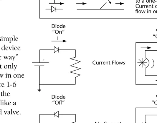
The diode is a simple semiconductor device acting as a “one way”
current valve. It only lets current flow in one direction. Figure 1-6 illustrates how the diode operates like a
“one-way” fluid valve.
(Purists please note:
This book does not use electron current flow.
All electrical current flow will be “positive” or
“conventional” current flow, meaning current
always flows from the most positive terminal to the most negative terminal of a component. The use of positive current flow follows the intuitive direction of the arrows inherent in the component drawings for diodes, transistors, etc.)
Transistors
The flow analogy can also be used to model how a transistor operates in a logic circuit. The transistor is an amplifier. It uses a small amount of energy to control a larger energy source, just as a valve controls a high-pressure water source.
There are two kinds of transistors: bipolar and field-effect transistors (FETs).
We will look at bipolar transistors first; these amplify current. A small amount
No Current Flows
Valve
“Closed”
Diode
“Off”
+
Current Flows
Valve
“Open”
Diode
“On”
+
Current Diode is analgous
to a one-way valve.
Current can only flow in one direction.
Figure 1-6: A diode to electricity is analogous to a valve in the flow of a fluid.
of current flows in the control circuit (the transistor base- emitter circuit) to turn the tran- sistor on. This control current is amplified (multiplied by the gain or beta of the transistor) and allows a larger current to flow in the output circuit (the collector- emitter circuit). Once again, the device is not perfect because of the resistance, current, gain, and
leakage limitations of real transistors. Bipolar transistors come in two polari- ties, NPN and PNP, with the difference being the direction in which current flows for normal operation. A
bipolar PNP transistor is shown and modeled in Figure 1-7.
For most of the illustrative circuit examples in this book, we will be using NPN transistors, as shown in Figure 1-8.
Mechanical Switches
Mechanical switches are useful for direct input to digital circuits. One of the more convenient versions is a bank of rocker switches packaged into a module that can fit into the same location as a standard chip. The dual in-line package, or DIP, switch is one of the easiest ways to add multiple switches to a micro- controller design. The mechanical switch has extremely low “on” resistance and high “off” resistance, unlike most semiconductor switches. Figure 1-9 shows a typical DIP switch and the schematic symbol for it.
Emitter PN P
Control Base
Current Flow Collector
“Sink”
“Source”
Current Flow
Figure 1-7: Operation of a bipolar PNP transistor.
Emitter NP N
Control Base
Current Flow Collector
“Sink”
“Source”
Current Flow
Figure 1-8: Operation of a bipolar NPN transistor.
OFF ON
Figure 1-9: 8-position DIP switch and schematic equivalent.
Transistor Switch ON
Transistors can be configured to function as switches. As can be seen in Figure 1-10, an NPN transistor operating as a current controlled switch can be used to build a simple inverter. It changes a logic one on its input to a logic zero at its output, and vice versa. In this case, logic one is represented as a positive voltage, and a logic zero is represented by zero volts. The logic one input (positive input voltage) is supplied through a resistor from the power supply voltage to the transistor base terminal, resulting in a small base control current into the base.
The transistor is used because it has gain allowing a larger output current to flow as controlled by a weaker input. When the transistor is turned on as much as it can be, the collector emitter circuit looks almost like a short circuit, effectively connecting the output to ground or zero volts. This gives a logic zero on the collector output. When the transistor collector is shorted to ground, current flows from the supply through the resistor and into the transistor collector to ground. The transistor is said to sink the resistor current into ground. If there is an external load, such as another inverter or gate, connected to the collector output, the transistor can also sink current from the load. This is also referred to as pulling down the output voltage.
The current sinking capacity of the transistor limits the number of devices this inverter can drive.
“1”
+
“0” “1”
+
“0”
Transistor (shorted)ON Resistor Sources Current
Output Sinks Current Transistor Inverter
Input 1 -> Output 0
Transistor Switch “ON”
Transistor (shorted)ON
Output Sinks Current Transistor Inverter
Equivalent Circuit
Equivalent Circuit
Figure 1-10: The transistor inverter; input = 1 and transistor ON. The transistor ON configuration is at left and the equivalent circuit is at right.
Transistor Switch OFF
When the input is connected to logic zero (ground voltage), no current flows into the base of the transistor, since its base and emitter terminals are at the same voltage. When there is no current flowing in the base, the transistor will not allow current to flow in the collector emitter circuit either. As a result, the circuit behaves as if the transistor was removed from the circuit. The output resistor will source current to any potential load. The output is pulled up to the supply voltage, resulting in a logic one at the output. Once again, there is a limit to the resistor’s ability to source current, resulting in a limit to the number of loads that can be attached to this circuit’s output. Notice these two limits are defined by the ability of the transistor to pull down the output, and the resistor’s ability to pull up the output become the main limits to its ability to drive other devices. Gates can be constructed by adding diodes or transis- tors to the inverter circuit in Figure 1-11.
The FET as a Logic Switch
Most of the logic devices used in highly integrated circuits do not use bipolar tran- sistors. Instead, they use field effect transistors. FETs perform a similar function to the bipolar transistors discussed earlier, but they are voltage
controlled. While the current flowing in the base controls bipolar transistors, the voltage between the gate and source controls field effect transistors. The gate voltage of a field effect transistor controls the current flowing in the drain-source circuit. The symbol for the FET shows the gate to be insulated from the source-drain circuit, as shown in Figure 1-12.
“0”
+
“1” “0”
+
“1”
Transistor OFF(open)
Resistor Sources Current
Input Sinks Current
Transistor Inverter Input 0 -> Output 1
Transistor Switch “OFF”
Transistor Inverter Equivalent Circuit
Equivalent Circuit
Resistor Sources Current
Transistor OFF(open)
Figure 1-11: The transistor inverter; input = 0 and transistor OFF.
The transistor OFF configuration is at left and the equivalent circuit is at right.
Drain
Source Gate
Figure 1-12: Field effect transistor (FET) schematic diagram.
This type of FET is referred to as a MOSFET (metal oxide semiconductor FET), since the insulating material is silicon dioxide (SiO2), commonly known as glass (for early devices, the gate was made
of metal). Like bipolar NPN and PNP transistors with opposite polarity, FETs come in N- and P- channel varieties.
The N- and P- channels refer to the polarity of the source drain element of the device. A cross-section view of a FET is shown in Figure 1-13.
NMOS Logic
The conductive state of the FET’s channel is what allows or prevents current from flowing in the device. For a typical logic N-channel MOSFET, the channel becomes conductive when the gate has a positive voltage with respect to the source, allowing current to flow between the drain and source terminals. When the gate is at the same voltage as the source, no current flows. The design of MOS logic circuits can be almost exactly equivalent to the bipolar inverter we saw earlier, substituting an N-channel MOSFET for the bipolar NPN transis- tor. In fact, the most of the early microcontroller integrated circuits were manufactured using variations of this method, and are referred to as NMOS logic. As can be seen from Figure 1-14, the NMOS FET circuit behaves in an equivalent way to the NPN transistor inverter. When the gate (control input) of the NMOS FET is at a positive voltage, the FET is ON, effectively shorting the source and drain pins. When the gate is at 0 volts, the FET is OFF, open- ing the circuit between the source and drain. Older NMOS logic ICs use this type of circuit. The original 8051 microcontroller was an NMOS processor.
Drain
Conductors Conductor
Channel Gate
SiO2
Insulator
Source
“1”
+
“0” “1”
+
“0”
NMOS FET Inverter Input 1 -> Output 0
NMOS FET (shorted)ON
Resistor Sources Current
Output Sinks Current NMOS FET Inverter
Input 1 -> Output 0
NMOS FET OFF(open)
Figure 1-14: NMOS inverter circuit.
Figure 1-13: Field effect transistor cross-section.
CMOS Logic
CMOS logic (complementary symmetry MOS) is another form of MOS logic.
It has advantages over NMOS logic for low power circuitry and for very complex integrated circuits. NMOS logic is relatively simple, but it has one serious draw- back: it consumes a significant amount of power. In fact, it would be impossible to manufacture the largest ICs using NMOS logic, as the power dissipated by the chip would cause it to overheat. This is the main reason CMOS logic has become the dominant form of logic used for large, complex ICs. Instead of using a resistor to source current when the output is high, a CMOS device uses a P-channel MOSFET to pull the output high. CMOS logic is based on the use of two complementary FETs that switch the output between the power supply and ground. A simple CMOS inverter is shown in Figure 1-15.
CMOS logic uses two switches: one P-channel pull-up transistor, and one N-channel pull-down device to pull the output low or high, one at a time.
CMOS logic is designed with an N-channel device that turns on and conducts when the gate voltage is at logic one (positive voltage), and the P-channel device turns on when the gate is at ground voltage. A CMOS inverter is com- prised of a pair of FETs, one device of each type, as shown in Figure 1-15.
When the transistor gate inputs are at logic one (positive voltage), the
P-channel device is off, and the N-channel device is on, effectively connecting the output to ground, or logic zero. Likewise, when the input is grounded, the P-channel device turns on and the N-channel device turns off, effectively connecting the output to the positive supply voltage, or logic one. Gates and more complex logic functions can be constructed by using series and parallel- connected MOSFETs in circuits similar to the one above. The gate of a
CMOS Inverter
N FET OFF N FET ON
Sinks Current
P FET ON Sources Current Output LOW Output HI Output
P FET OFF P-channel
Power
Equivalent
Output LOW Equivalent Output HI
N-channel Ground Input
+
Figure 1-15: CMOS inverter circuit and equivalent output.
MOSFET, as implied by the symbol, is essentially an open circuit. In fact, the gate of a MOSFET does have an extremely high resistance. The operation of the MOSFET’s channel is controlled by the voltage of the gate, unlike the bipolar NPN transistor we examined in the inverter, which is controlled by input (base) current. Bipolar transistors are current amplifiers, with their output current being controlled by their base current. FET outputs, on the other hand, are dependent on the gate voltage.
Since almost no current flows in a CMOS output when it is driving a CMOS gate input in the steady state condition, these logic devices consume much less power than the other types. MOS logic has some other advantages over bipolar logic, since there is almost no input current (less than one nanoampere, or 10-9 ampere), so it does not need to exact a DC current load on the device driving it. This is good news, because it means that the input current of a CMOS device does not limit the number of gates that can be connected to the output of the driving gate. The number of gate inputs that a single gate output can drive is the gate fan-out. Fan-out applies between gates of the same logic family, as different families of logic have different output capabilities and their inputs present different loads.
Now for the bad news about the high input resistance of MOS devices: the insulation separating the input from the channel is very thin (measured in angstroms). This thin layer can easily be punctured by electrostatic discharge (ESD), such as occurs regularly when dissimilar materials rub against one another. Just walking across the room can generate tens of kilovolts, which is more than enough to destroy a MOS device. As a result, special precautions must be taken to prevent damage to MOS devices. When handling these devices, it is important to ground your body before touching the device, and to also keep the device at or near ground. Special wrist straps and workspace mats are available to assist in keeping static voltages from building up and for dissipating them when they do occur. Special, conductive bags and containers should be used when possible to contain sensitive devices.
CMOS power consumption is usually dominated by the power consumed dur- ing the transition of a logic device from one state to another. As a result, pure CMOS devices consume only a few microamperes of current when they are not switching, and the bulk of the current drawn is a function of clock frequency.
The higher the clock frequency, the greater the current consumption. For pure CMOS, the power supply current is linearly proportional to the clock rate.
Mixed MOS
Many logic devices labeled as CMOS are actually a mixture of NMOS and CMOS, because the manufacturer needs to compromise the extremely low power of CMOS with the performance of NMOS logic. This can be a problem for design- ers of battery-powered systems, since the current requirement (and the resulting battery life) of a pure CMOS circuit is orders of magnitude better than an NMOS circuit. Many CMOS memories are actually mixed MOS, and are not appropri- ate for battery-powered systems. True CMOS chips can retain their contents for years using only a single coin cell to maintain power to the memory.
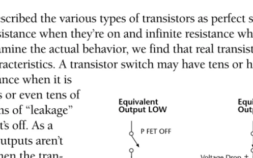
Real Transistors Don’t Eat Q!
So far we have described the various types of transistors as perfect switches that have zero resistance when they’re on and infinite resistance when they’re off. When we examine the actual behavior, we find that real transistors do not exhibit these characteristics. A transistor switch may have tens or hundreds of ohms of resistance when it is
on, and hundreds or even tens of thousands of ohms of “leakage”
resistance when it’s off. As a result, the logic outputs aren’t perfect either. When the tran- sistor is on, the output voltage is a function of the output current, due to the voltage drop across the resistance. As Figure 1-16 shows, the output voltage of a logic device will depend upon how much cur- rent is flowing in the output and the resistance of the switch.
Unfortunately, the switch resistance is also non-linear so that the switch resis- tance changes as the voltage across the switch changes. This makes it difficult to picture the output behavior under different operating conditions. The behavior will also differ from one device to another, over temperature, and so on. Manufacturers only specify the output characteristic at one point on the
+ –
+ –
N FET OFF N FET ON
Sinks Current
P FET ON Sources Current
Output LOW Output HI
P FET OFF
Voltage Drop across Switch Resistance
Equivalent
Output LOW Equivalent
Output HI
Voltage Drop across Switch Resistance
Figure 1-16: Logic output voltage is current dependent.
curve, Vo at Io max. As a result, the best we can do is to look at the output characteristics graphically, as shown in Figure 1-17.
Logic Symbols
Logic symbols are used to represent the logic functions in a more abstract way, allowing the designer to specify the logical function of a circuit without getting into the details of the underlying components (such as the transistors and resistors). The logic symbols used in this text represent those that are most commonly used in commercial documentation. There are other standards, such as the ANSI/IEEE standard gate level symbols, but they are not encountered as frequently in practice. Figure
1-18 shows the logic symbols for different gates, and their functions are described in the truth tables.
The logic symbols in Figure 1-18 show the shapes and Boolean logic functions for the most common gate configurations. The buffer device is a triangle—the symbol for an amplifier—because it amplifies the input signal, allowing an increase in the number of loads that can be driven. Note that a small circle, often referred to as a
“bubble,” on an input or output terminal designates a logical inver- sion. Thus the inverter is shown as
a triangle (amplifier) with a bubble on the output to signify the logic level inversion on the output. The logic voltage levels for TTL logic are:
Positive Logic Corresponding TTL Logic Voltages 0 = false = lowest voltage level 0 = input voltages 0 to 0.8 volts (low) 1 = true = highest voltage level 1 = input voltages 2 to 5 volts (high)
VOH VOL
Vcc
VOL max IOL IOL max
IOH max VOH max
-IOH
Figure 1-17: Output voltage Vo versus current Io.
A B F 0 0 1 0 1 1 1 0 1 1 1 0 NAND F = AB
A B F 0 0 1 0 1 0 1 0 0 1 1 0 NOR F = A+B
A B F 0 0 1 0 1 0 1 0 0 1 1 1 XNOR F = A+B A
B F A
B F A
B F
A F 0 1 1 0 Inverter F = A
A F
A B F 0 0 0 0 1 0 1 0 0 1 1 1 AND F = AB
A B F 0 0 0 0 1 1 1 0 1 1 1 1 OR F = A+B
A B F 0 0 0 0 1 1 1 0 1 1 1 0 XOR F = A+B A
B F A
B F A
B F
A F 0 0 1 1 Buffer F = A
A F
Figure 1-18: Logic symbols, symbolic notation, and truth tables.
This means that a TTL compatible logic input is guaranteed to respond to an input signal between 0 and 0.8 volts as a logic zero, and input voltages from 2 to 5 volts as a logic one. Note that voltages between 0.8 and 2 volts are not valid logic levels.
Logic voltage levels are different for different types of logic, but the most common logic levels are those corresponding to the original TTL (transistor- transistor logic), using a 5 volt power supply. CMOS levels, using 3 or 5 volt power, are also common. TTL and CMOS logic—like almost every other type of logic in common use —are called positive logic because the most positive voltage corresponds to the logic one value.
Tri-State Logic
Tri-state logic does not refer to orderly thinking in a three state geographic region! When we speak of binary (base two number) values, we mean that a given bit or logic signal can take on either one of two valid states (zero or one) at any instant in time. A logic gate that is not forcing its output to be either one or zero is said to be tri-stated. Tri-state logic does not refer to base three numbers, but rather to a third invalid logic state when the output of a logic device is neither sinking nor sourcing current. This so-called third state is really an undefined
condition, because the device output is not forcing a logic level on its output. It is said to be in a floating, high imped- ance, passive, or Hi-Z state, since the output circuits are effectively disconnected. A tri-state driver connected to one signal wire of the bus is shown in Figure 1-19.
On the left is an inverting buffer with an enabled tri-state output. On the right side is an example showing two of the same type of buffers, with the top device in the disabled or passive state, and the lower device is enabled
A Y
A OE Y
0 1 1
1 1 0
0 0 ?
1 0 ?
Tri-State Inverting Buffer Output ENabled Output DISabled
Input Output OE
A A
1
?OFF HI-Z A
0
NC
Hi-Z Hi-Z
Output Switch (closed)ON
Output Switch (open)OFF Truth Table
Symbol and Function Equivalent Circuit – Active and Passive Figure 1-19: Active and passive states of a tri-state buffer.
or actively driving the data bus to a logic one level. The control signal deter- mines whether the output is passive or active, and is called the output enable or OE signal. The device shown above is actively driving the bus whenever the OE control line is at a logic one level, and is passive when the OE line is at a logic zero level. Most of the time, output enable signals are active low, mean- ing that the output is enabled when the /OE signal is low, and passive when the /OE signal is high. This is shown on the logic symbol with an inversion bubble where the enable signal enters the logic device.
As computer circuits become more dense and complex, the connecting wires have become increasingly difficult to route and interconnect. This is especially true on a densely packed integrated circuit, where it turns out that the wiring is more valuable than the logic gates! On one common CPU chip, 68% of the chip area is used for interconnect wiring. Even on a circuit board, it is impor- tant to use the board wiring in an efficient way. Since there are many parallel address and data lines that must go to multiple chips, the multiplexing approach makes it practical to connect many devices. The purpose for using tri-state logic is to allow multiple devices to share wires by taking turns one at a time.
This may sound a bit silly, but it is just one form of multiplexing, or sharing a resource that needs to be allocated among multiple devices. When the resource is a collection of parallel data wires, referred to as a data bus, and the bus is shared by multiple microcomputer CPU and peripheral devices transferring information one at a time in sequence, it is referred to as a multiplexed data bus.
Timing Diagrams
The timing diagram is the standard “language” of illustrating timing relation- ships between different parts of a design. In order to understand the relation- ship of different signals with respect to time, it is necessary to learn how to read and interpret timing diagrams. Figure 1-20 shows examples of asynchro- nous (un-clocked or combinatorial gates) and synchronous (clocked flip-flop) logic. The notation used in this book is representative of that used in most component specifications. Timing specifications, such as delay, setup, and hold times, specify the limits under which the device is guaranteed to operate as intended. If those specifications are violated, the device may very well operate correctly most of the time. However, a change in temperature, voltage, or variations from unit to unit may make the circuit unreliable. The most
undesirable result of timing violations is that the circuit makes very infre- quent errors, perhaps one error in hundreds of hours of operation. If you have ever wondered why your PC crashes mysteriously for no apparent reason, timing specification violations may well be the cause!
Timing relationships are particularly important for signals that are “time shared”
on a single wire. A group of wires that carries different information at different times is also called a bus.
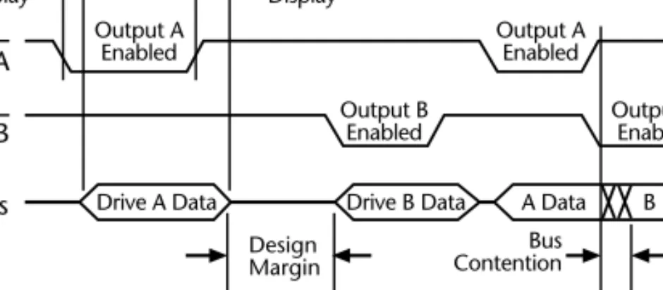
Multiplexed Bus
In order to describe the timing of such a shared data bus, it is neces- sary to define some notation for timing diagrams. The notation used in this book is shown in Figure 1-21.
The terminology for timing param- eters is covered in a later chapter, but the basic concept for time multiplexed data on a bus is shown in Figure 1-21. The two devices are alternately enabled to drive the data bus wire, allowing each to drive the bus in turn. Only one device is allowed to drive the bus at a time when it is operating correctly.
NAND A
B F
CK NOR
D Q
Q
Hold
Setup Delay
A F B
RiseTime
Delay
Fall Time
CK
D
Q
Q A
B
F=A*B
G=A+B
Figure 1-20: Timing diagram notation examples.
Data from A
Tri-State Data Bus To Other Devices
DataBus to A
New Data from A
Data from B
A B new A
Device A
DA
OEA to BusData from A Enable Output A to Bus
Data Bus
BusData to B Device B
DB
OEB Datato Bus from B Enable Output B to Bus BUS
OEA
DA
OEB
DB
BUS
Figure 1-21: Time multiplexed data bus and timing.
Timing diagrams are a critical method to allow accurate and unambiguous representation of the time related operations of digital circuits, which we will be using to understand and document the correct sequence of operations for microcomputer systems. Timing analysis, using these diagrams, allows the designer to determine safe and reliable limits to proper operation of the various circuits in the system. It is better to take a little more time to design a circuit correctly from the start than it is to find and fix bugs during testing. This is especially true because of the increasing cost of fixing a bug as a product progresses through production and into the field.
Loading and Noise Margin Analysis
In addition to timing, the designer must consider the voltages and loads at the logic inputs and outputs. If the output of one gate is connected to the input of another, the designer must assure that the logic voltages are compatible. Once again, just as for the timing, violations of these specifications often result in infrequent errors that are very tricky to reproduce. Again, prevention is much simpler than tracking down bugs as they appear in production units. This topic is the subject of Chapter Three.
The Design and Development Process
Structured design of a microcomputer requires the ability to do the system design and partitioning from the top down while implementing the system from the bottom up. The hardware design and development process should consist of the following steps:
1) Defining the requirements.
2) Collecting information on potential components.
3) Evaluate the components with respect to the requirements.
4) Do a block diagram preliminary design and component selection.
5) Perform a preliminary timing and loading analysis.
6) Define the functions of the “glue logic.”
7) Schematic entry using CAD (computer-aided design) software.
8) Programmable logic device design and simulation.
9) Detailed timing analysis and simulation, adjusting the design as required.
10) Check the signal loading, buffering signals as needed.
11) Document the design and generate a net list and bill of materials.
12) Begin the design and layout of a printed circuit board.
13) Implement the design in breadboard or prototype form.
14) Program the memories and programmable logic as required for testing.
15) Debug and verify operation using oscilloscope, logic analyzer, and in-circuit emulator.
16) Update and complete documentation as the design changes.
The order of tasks shown is variable, and some of the tasks may be performed in parallel. Software design is also frequently done in parallel with hardware design, and sometimes even before the hardware design. This is frequently a result of the fact that the cost and time required to develop the software exceeds that of the hardware development. In some cases the cost of modifying existing programs may be so high as to be impractical. In these cases, it is the designer’s responsibility to maintain software compatibility with previous hardware designs.
Chapter One Problems
1. If an open-drain N-channel FET transistor is used as a logic output, is it possible to connect more than one open-drain transistor output to the same signal? What would the effect of doing so be on the resulting combined signal?
2. If a logic output sinks IOL = 10 milliamperes with an output voltage, VOL = 0.5 volts, how much power is dissipated by a 450 ohm resistor between the output and the 5 volt power supply?
3. How much current must a logic output source, in order to maintain an output voltage of 2.5 volt when driving a 5 kilohm resistor connected to ground?
4. In a CMOS inverter, there is a short period of time when both the N- and P-channel transistors are partially turned on when the input is changing from low to high or high to low. What effect will this have on power con- sumption? What characteristic in the input signal would reduce this effect?
2
One way of looking at a computer system is to consider the successive
“translations” that occur from the high level code (a programming language such as C++) to the electrical signals that “communicate” with the hardware.
A computer system can be broken down into multiple levels or layers to show the translation of a specific instruction into a form that can be directly pro- cessed by the computer hardware. Such hierarchical levels are discussed in detail in Structured Computer Organization by A.S. Tanenbaum. This hierarchy is shown in Figure 2-1
Language translators such as compilers and assemblers translate high- level code into machine code that can be executed by the processor. The primary focus of this book will be from the assembly and machine language level downward.
Microcontroller Concepts
High Level Assembly Machine Register Transfer Gate
Circuit
Sum := Sum + 1
MOV BX,SUM INC (BX)
1101010100001100 0010001101110101 1111100011001101 Fetch Instruction, Increment PC, Load ALU with SUM ...
CK
O O +
Figure 2-1: “Layers” of a computer system.
Organization: von Neumann vs. Harvard
We introduced the von Neumann and Harvard computer architectures in Chapter One. The von Neumann machine, with only one memory, requires all instruction and data transfers to occur on the same interface. This is sometimes referred to as the “von Neumann bottleneck.” In common computer architec- tures, this is the primary upper limit to processor throughput. The Harvard architecture has the potential advantage of a separate interface allowing twice the memory transfer rate by allowing instruction fetches to occur in parallel with data transfers. Unfortunately, in most Harvard architecture machines, the memory is connected to the CPU using a bus that limits the parallelism to a single bus. The memory separation is still used to advantage in microcontrollers, as the program is usually stored in non-volatile memory (program is not lost when power is removed), and the temporary data storage is in volatile memory.
Non-volatile memories, such as read-only memory (ROM) are used in both types of systems to store permanent programs. In a desktop PC, ROMs are used to store just the start-up or bootstrap programs and hardware specific programs.
Volatile random access memory (RAM) can be read and written easily, but it loses its contents when power is removed. RAM is used to store both application programs and data in PCs that need to be able to run many different programs.
In a dedicated embedded computer, however, the programs are stored permanently in ROM where they will always be available. Microcontroller chips that are used in dedicated applications generally use ROM for program storage and RAM for data storage. Memory technology is crucial to the design and understanding of embedded computers, and Chapter Four is dedicated to this important topic.
Microprocessor/Microcontroller Basics
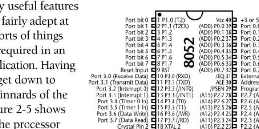
There are three groups of signals, or buses, that connect the CPU to the other major components. The buses are:
• Data bus
• Address bus
• Control bus
The data bus width is defined as the number of bits that can be transferred on the bus at one time. This defines the processor’s “word size.” Many chip vendors define the word size based on the width of an internal data bus. For the purposes
of this book, however, a processor with eight data bus pins is an 8-bit CPU. Both instructions and data are transferred on the data bus one “word” at a time. This allows the re-use of the same connections for many different types of information.
Due to packaging limitations, the number of connections or pins on a chip is limited. By sharing the pins in this way, the number of pins required is reduced at the expense of increased complexity in the external circuits. Many processors also take this a step further and share some or all of the data bus pins to carry address information as well. This is referred to as a multiplexed address/data bus. Processors that have multiplexed address/data buses require an external address latch to separate and hold the address information stable for the duration of a data transfer. The processor controls the direction of data transfer on the data bus.
The address bus is a set of wires that are used to point to the memory or I/O location that is to be read from or written to. The address signals must gener- ally be held at a constant value for some period of time before, during, and after the data is transferred. In most cases, the processor actively drives the address bus with either instruction or data addresses.
The control bus is an assortment of signals that determine what kind of informa- tion is on the data bus and determines where the data will go, in conjunction with the address bus. Most of the design process is concerned with the logic and timing of the control signals. The timing analysis is primarily involved with the relative timing between these control signals and the appearance and disappearance of data and addresses on their respective buses.
Microcontroller CPU, Memory, and I/O
The interconnection between the CPU, memory, and I/O of the address and data buses is generally a one-to-one connection. The hard part is designing the appropriate circuitry to adapt the control signals present on each device to be compatible with that of the other devices. The most basic control signals are generated by the CPU to control the data transfers between the CPU and memory, and between the CPU and I/O devices. The four most common types of CPU controlled data transfers are:
1) CPU reads data/instructions from memory (memory read)
2) CPU writes data to memory (memory write)
3) CPU reads data from an input device (I/O read) 4) CPU writes data to an output device (I/O write)