An Integrated Sigma-Delta Noise-Shaped Buck Converter
Wei-Hsun Chang *, Yung-Hsin Jen **
Dept. of Electrical Engineering National Cheng Kung University
Tainan, Taiwan
E-mail: n28981280@mail.ncku.edu.tw*
n2695457@mail.ncku.edu.tw**
Chien-Hung Tsai Dept. of Electrical Engineering National Cheng Kung University
Tainan, Taiwan E-mail: chtsai@ee.ncku.edu.tw
Abstract—An integrated sigma-delta noise-shaped buck converter that uses a discrete-time second order single-bit sigma- delta modulator (DT-SDM2) is presented. The DT-SDM2 buck converter and a compared PWM controller are designed and fabricated on a standard TSMC 0.35μm 3.3V CMOS process.
The operating frequency of the proposed DT-SDM2 ranges from 400 KHz to 1.2 MHz. Simulation results show that DT-SDM2 has better noise performance than those of PWM and continuous- time SDM2 (CT-SDM2) buck converters.
Keywords-component; buck converter; sigma-delta; noise- shaped
I. I NTRODUCTION
Tiny, highly-efficient, and low-noise power management ICs are indispensable for modern portable electronic products such as cellular phones and personal digital assistants.
Traditionally, a switch-mode power converter (SMPC) with a fixed-frequency PWM (pulse width modulation) controller has been used to achieve high conversion efficiency. However, a fixed-frequency control technique inevitably results in the appearance of a ripple voltage at the same frequency at the output of SMPC. For modern SoC with embedded RF, analog/mixed-signal, digital, and power management IPs, this ripple is highly undesirable because its associated harmonic content can couple via the substrate and supply lines to corrupt and degrade the performance of sensitive RF and analog circuits [1].
In order to suppress the influence of the discrete spurious content associated with PWM SMPC, 2
ndorder sigma-delta modulator (SDM2) based buck converters have been presented [1][2]. They spread the tonal content to higher frequencies (the so-called “noise-shaping”) and reduce the in-band switching noise of the buck converter. For the implementation of SDM, both continuous-time (CT) and discrete-time (DT) methods can be adopted. However, compared with the mature DT- SDM, it should be noted that CT-SDM is by nature more suitable for high-frequency operation and usually involves complex design issues [3]. In addition, modern SMPCs typically operate from several hundred kHz to several MHz.
DT-SDM is thus adapted in this research to implement an integrated noise-shaped buck converter.
In general, published low-noise integrated buck converters [1][2] are weak or lack a complete top-down design
methodology starting from system modeling to circuit implementation. This paper attempts to bridge this gap by focusing on the design and implementation of a fully integrated buck converter based on a 2
ndorder, single-bit DT-SDM (DT- SDM2) controller.
II. A RCHITECTURE OF DT-SDM2 B UCK C ONVERTER The system block diagram of the DT-SDM2 buck converter is shown in Fig. 1. The converter IC includes: a power stage, an output voltage divider, an error amplifier (with compensation), a DT-SDM2 controller, and a gate driver buffer (with dead-time control). The synchronous rectifier architecture is used for enhancing the power conversion efficiency. Dead-time control and the gate driver circuit are designed to generate non-overlapping power-MOS control signals to avoid shoot-through current flows from the supply to ground. The inductor and capacitor of the power stage form a low-pass filter to effectively suppress SDM generated high- frequency shaped output noise. The converter’s output voltage V
outis scaled down to bV
outvia feedback resistors, R
FB1and R
FB2, and compared with reference voltage V
refbefore being fed into the error amplifier. The error amplifier not only magnifies the error signal, which equals bV
out- V
ref, but also can provides enough loop-gain to achieve a smaller V
outsteady-state error. The Z
1/Z
2network forms a loop- compensator to ensure system stability. V
Coutput from the compensator passes through the DT-SDM2 controller and generates noise-shaped gate drive signal V
ctrl, which is a pulse- density modulated (PDM) signal.
Z1
+ Vin-
S1
S2
Controller
L RL
RC
C Rload
+
- Vout
RFB1
RFB2
Vref
Compensator
VC Second Order
Δ modulator Power Stage
Vctrl
Z2
Dead-Time Control and Driver Circuit
bVout
Fig.1 System block diagram of the DT-SDM2 buck converter.
PEDS2009
18
The block diagram of the DT-SDM2 converter used in this paper is shown in Fig. 2. It mainly consists of 2 integrators, a 1-bit quantizer, and a DAC. As can be seen, the analog input signal V
Cis compared with the feedback digital signal Q(t) to generate the error signal. After this error signal passes through the two integrators, the output signal Y
2of the second integrator is quantified by a 1-bit (2-level) quantizer. The quantizer is modeled by an equivalent input quantization noise source E and an generated 1-bit digital output signal V
ctrlwith logic level “High” or “Low”. For a stable SDM, after some initial-transients, the averaged output V
ctrleventually equals input V
C[3]. The relationship between input V
Cand the output V
ctrlis shown in (1), where Q
VHdenotes the number of occurrences that V
ctrl= “High” and Q
VLdenotes the number of occurrences that V
ctrl= “Low”. A large input V
Cleads to a large number of occurrences of V
ctrl= “High”. The corresponding duty cycle D of the DT-SDM2 controller is shown in (2).
VL VH
VL VH
C
Q Q
Q V Q
+
= − (1)
VL VH
VH
Q Q D Q
= + (2)
Fig. 2 Block diagram of DT-SDM2.
According to Fig. 2, the transfer characteristic can be easily derived as (3). It is clear that the input transfer function, V
ctrl(z)/V
C(z), is a low pass filter. This indicates that the in- band low-frequency input signal will pass to the output with an additional two sample delay z
-2; the “quantization” transfer function, V
ctrl(z)/E(z), is a high pass filter which means that the in-band quantization noise will be pushed to higher out-of- band frequencies. Noise-shaping is thus achieved. Finally, the high-frequency quantization noise is filtered and suppressed by the LC low-pass filter in the power stage, producing a low- noise output voltage.
( ) ( )
( 2 ) ( 1 ) ( )
1
) 1 (
) 1 (
2 ) 1
(
2 2 2 1 1 2
2 1
2 2 2 1 1 2
2 2 1
z z E a a a z a
z
z z V a a a z a
z a z a
V
ctrl C⋅ ⋅ +
−
⋅ +
⋅
− + + −
⋅ ⋅ +
−
⋅ +
⋅
− +
⋅
= ⋅
−
−
−
−
−
−
(3)
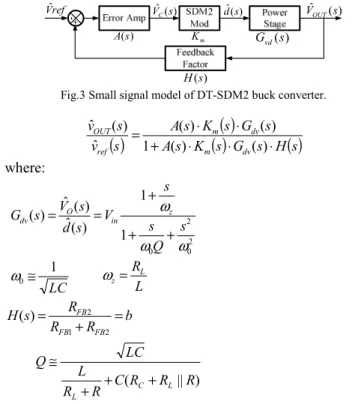
III. SYSTEM M ODELLING AND C OMPENSATOR D ESIGN Fig. 3 shows the small-signal model of the proposed DT- SDM2 buck converter for system analysis, where H(s) denotes the divider ratio of feedback resistors, R
FB1and R
FB2, A(s) denotes the transfer function of the compensator, G
vd(s) denotes the control-to-output transfer function, and K
m(s) is the equivalent s-domain transfer function (i.e. duty cycle) of DT-SDM2. An SDM2 block is used here to replace the traditional PWM block. Consequently, the overall system
closed-loop transfer function of the DT-SDM2 buck converter can be written as (4) [4].
ref
Vˆ Vˆ sC() dˆ s() VˆOUT(s) )
(s
A Km
G
vd(s )
) (s H
Fig.3 Small signal model of DT-SDM2 buck converter.
( ) ( )
( ) s G s H ( ) s
K s A
s G s K s A s
v s v
dv m
dv m ref
OUT
⋅
⋅
⋅ +
⋅
= ⋅
) ( )
( 1
) ( )
( ˆ
)
ˆ ( (4)
where:
2 0 2 0
1 1 )
ˆ ( ) ˆ ( ) (
ω ω
ω s Q s
s s V
d s s V
G
dv O in z+ +
+
=
=
LC 1
0
≅
ω ω
z= R L
LR b
R s R H
FB FB
FB
=
= +
2 1
)
2(
)
||
( R R R R C
R L Q LC
L C L
+ + +
≅
A. Modelling of SDM2 controller
To design the DT-SDM2 buck converter with an optimum phase margin and loop-bandwidth (i.e. cross-over frequency), all of the transfer functions in (4) must be known in advance.
The transfer function of a traditional PWM block can be modeled by 1/V
PP, where V
PPis the peak to peak amplitude of a triangle wave generated by the corresponding ramp generator [5]. However, it is unclear whether this can be used to model the DT-SDM2 block because SDM is actually modeled in the z-domain, which is not compatible with the other blocks modeled in s-domain. Hsieh [6] proposed an equivalent 1
storder SDM model, but the results cannot be applied to model a 2
ndorder SDM. Using the assumptions of [6], we modify and derive the equivalent s-domain model of the SDM2 block k
m(s) as shown in (5), where V
qis half of the step size of the DAC output in the feedback path of Fig. 2. For the final DT-SDM2 design, a
1=a
2=0.5 is chosen. The equivalent s-domain transfer function can thus be model by 1/6V
q. It is worth mentioning that applying our modified method to re-derive the SDM1 model produces results identical to those shown in [6].
q C
m
a V
a s
v s s d
G = = ⋅ + ⋅
) 1 ( 2 )
~ ~ ( ( ) ) (
1
1
(5) As mentioned, two additional sampling delays appear in the SDM2 signal path, inevitably introducing an extra time delay in the converter. This extra time delay degrades the system’s phase-margin. The induced additional phase lag is shown in (6) [1], where f
sis the sampling frequency and f
cis the system’s cross-over frequency.
PEDS2009
19
S C
f phase f
additional = 360 2 ⋅ ° ⋅
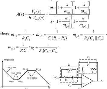
(6) B. Compensator Design
If G
dv(s), H(s), and k
m(s) are known, the system’s cross-over frequency f
cand the compensator’s transfer function A(s) can be properly chosen and designed. From (6), a smaller f
cimproves the phase margin, but it results in a slower transient response. Here, we compromise by chosing f
c= 40 kHz as the design specification. For the intended sampling frequency target of 400 kHz to 1.2 MHz, the maximum phase lag is less then 12°. For a normal 60° phase margin design, this is a reasonable requirement.
To obtain a high DC gain and a small steady-state error, the compensator should have a pole at the origin. In addition, for properly compensating pairs of conjugate poles of G
dv(s) ((4)), the compensator should have two low-frequency zeros (ω
cz1, ω
cz2) to stabilize the system. The compensator should also contain one pole (ω
cp1) for cancelling the zero of G
dv(s) to avoid increasing high-frequency noise and another pole ( ω
cp2) to further decrease the noise at higher frequencies. A compensator with three poles and two zeros (i.e. type ІІІ compensator [7]) that satisfies all the above requirements is shown in Fig. 4. Poles and zeros of a type ІІІ compensator can be matched to elements using (7).
⎥ ⎥
⎦
⎤
⎢ ⎢
⎣
⎡ +
⎥ ⎥
⎦
⎤
⎢ ⎢
⎣
⎡ +
⋅
⎥ ⎦
⎢ ⎤
⎣
⎡ +
⎥ ⎦
⎢ ⎤
⎣
⎡ +
⋅
⋅ =
=
2 1
2 1
1 1
1 1
) (
) ) (
(
cp cp
cz cz
I
out C
s s s
s s
s V b
s s V
A
ω ω
ω ω ω
(7)
where
2 2 1
1 C
cz
= R
ω ,
) (
1
3 1 1
2
C R R
cz
= +
ω ,
)
||
( 1
3 2 2
1
R C C
cp
=
ω ,
1 1 2
1 C
cp
= R
ω ,
(
2 3)
3
1 C C
I
R
= +
ω .
C2
R1
R2
C3
C1
R3
b·Vout
VC
Z1
Z2
Vref
(b)
Fig. 4 (a) Poles and zeros of compensator. (b) Type ІІІ compensator.
IV. C IRCUIT D ESIGN A ND I MPLEMENTATION
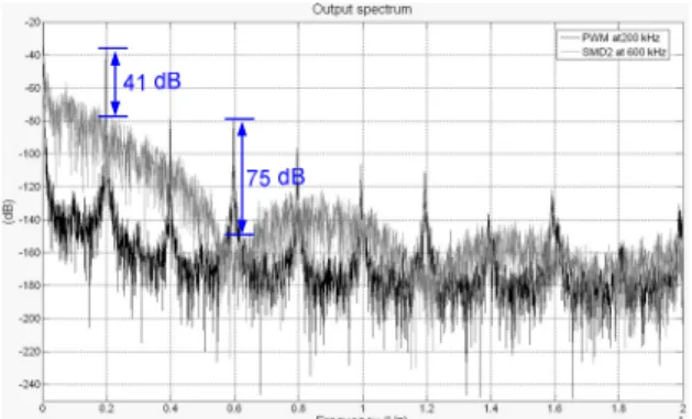
The circuits were designed and fabricated using a standard 0.35μm 3.3V CMOS process, as shown in Fig. 5. To verify that the DT-SDM2 buck converter has good noise performance, a conventional PWM controller was added in the implementation for comparison. Switch S
Vmodeis used to switch between SDM and PWM operating modes. The DT- SDM2’s transfer function (k
m(s)=1/6V
q) and the PWM’s transfer function (1/V
PP) were designed to be similar. This consideration produces a relatively fair comparison environment. As shown in Fig. 7, the DT-SDM2 consists of three opamps, one quantizer, one static latch, one four-phase
clock generator, and some feedback control logics. Most of the important design specifications, the corresponding guidelines, and design-values are briefly summarized in Table I, where Δ denotes the step size of the DAC in the feedback path of SDM2, β is the closed-loop feedback factor of the OPAMP, T
S=1/(1.2·10
6) is the worst-case sampling period, ε
sdenotes the sampling error, and k is the Boltzmann constant. As mentioned in Section III-B, f
c= 40 kHz was chosen. The highest sampling frequency is 1.2 MHz, so the over-sampling ratio (OSR) is about 94 in our design. The layout of the DT- SDM2 buck converter is shown in Fig. 6, where the chip area is 1.57 mm
2and the area of the DT-SDM2 controller is about 0.37 mm
2.
DT-SDM2 controller
CK3 OP OP
CK1 CK4
CK3 CK1 CK2
CK4 CK2
Vref- Vref+
CKA CKB
Static Com Latch Y Y
CK2Y CKA
CK2Y CKB
Feedback Control Logic
CK4 Vref- Vref+
CKB
OP CKA
Com
PWM controller SVmode
SVmode CK1 CK2 CK3 CK4
Analog_gnd
Ramp Generator
VC
Vctrl
CS CS
Cf Cf