行政院國家科學委員會專題研究計畫 成果報告
毫微米電晶體在高頻除三除頻器電路的應用性研究(I) 研究成果報告(精簡版)
計 畫 類 別 : 個別型
計 畫 編 號 : NSC 97-2221-E-011-138-
執 行 期 間 : 97 年 08 月 01 日至 98 年 07 月 31 日 執 行 單 位 : 國立臺灣科技大學電子工程系
計 畫 主 持 人 : 張勝良
計畫參與人員: 博士班研究生-兼任助理人員:劉政辰 博士班研究生-兼任助理人員:張珈瑋
處 理 方 式 : 本計畫涉及專利或其他智慧財產權,2 年後可公開查詢
中 華 民 國 98 年 09 月 14 日
行政院國家科學委員會補助專題研究計畫 █ 成 果 報 告
□期中進度報告 毫微米電晶體在高頻除三除頻器電路的應用性研究(I)
計畫類別: 個別型計畫
□
整合型計畫計畫編號:NSC 97-2221-E-011-138
執行期間:2008 年 08 月 01 日至 2009 年 07 月 31 日
計畫主持人:張勝良 教授 共同主持人:
計畫參與人員:劉政辰、張珈瑋
成果報告類型(依經費核定清單規定繳交):■精簡報告 □完整 報告
本成果報告包括以下應繳交之附件:
□赴國外出差或研習心得報告一份
□赴大陸地區出差或研習心得報告一份
■出席國際學術會議心得報告及發表之論文各一份
□國際合作研究計畫國外研究報告書一份
處理方式:除產學合作研究計畫、提升產業技術及人才培育研究 計畫、列管計畫及下列情形者外,得立即公開查詢 □涉及專利或其他智慧財產權,□一年□二年後可公 開查詢
執行單位:
中 華 民 國 98 年 8 月 25 日
1. 中文摘要
這篇文章提出一個寬鎖定範圍的除三注入鎖定除頻器,且已用聯 電90奈米1P9M金氧半技術製作完成。此除頻器由nMOS交相耦合 LC振盪器與兩個注入MOSFET串聯那交相耦合nMOSFETs所組 成。直接注入鎖定除頻器是由兩個線性的混波器形成且共享相同 的直流電流使得一個低功率的直接注入鎖定除頻器電路可以被 設計。在0.7伏特的電壓供應下,自我振盪頻率是從10.18~11.56 GHz,除頻器的電流與功耗不包含緩衝器,各別是2.8 mA和 1.96 mW。當注入功率為0 dBm時,總操作頻率是4.74 GHz,注入頻 率可從29.96 到34.70 GHz
關鍵詞:金氧半場效電晶體、壓控振盪器、除三直接注入鎖定除 頻器、寬鎖定範圍、變壓器
2. Abstract—This paper proposes a wide-locking range divide-by-3 injection-locked frequency divider (ILFD) fabricated in the 90nm 1P9M CMOS technology. The divider consists of an nMOS cross-coupled LC oscillator and two injection MOSFETs in series with the cross-coupled nMOSFETs. The ILFD is formed with two linear mixers which share the same dc current so that a low power ILFD can be designed. At the supply voltage of 0.7 V, the free-running frequency is from 10.18 to 11.56 GHz, the current and power consumption of the divider without buffers are 2.8 mA and 1.96 mW, respectively. At the incident power of 0 dBm, the total operational locking range is 4.74 GHz, from the incident frequency 29.96 to 34.70 GHz.
Keywords: CMOS, VCO, divide-by-3 injection-locked frequency divider, wide locking range, transformer.
3. Introduction
Injection-locked frequency dividers (ILFDs) are widely used as the sub-blocks of phase locked loop (PLL) and carrier recovery blocks. A popular ILFD is the LC resonator based circuit because the operating frequency can be very high and it consumes low power, and the center operation frequency of LC-tank ILFD is less sensitive to process variations than the inductor-less ILFDs. The even-modulus ILFDs include divide-by-2 [1-2] and divide-by-4 [3-4]
circuits and the odd-modulus ILFDs include divide-by-3 circuits
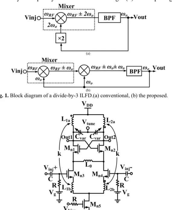
[5-8]. The divide-by-3 frequency divider often uses a second harmonic mixer, its function block is described in Fig. 1(a) and the locking range is generally narrow. In the simplified block diagram for the divide-by-3 frequency divider shown in Fig. 1(a), the frequency multiplicative element represents the nonlinearity of the mixer.
In this paper, we propose a new divide-by-3 ILFD using two linear mixers. The simplified block diagram for the proposed divide-by-3 frequency divider is shown in Fig. 1(b). The input signal
(a)
(b)
Fig. 1. Block diagram of a divide-by-3 ILFD.(a) conventional, (b) the proposed.
Fig. 2. Schematic of the proposed divide-by-3 injection-locked frequency divider.
Fig. 3. Chip photo of the divide-by-3 ILFD.
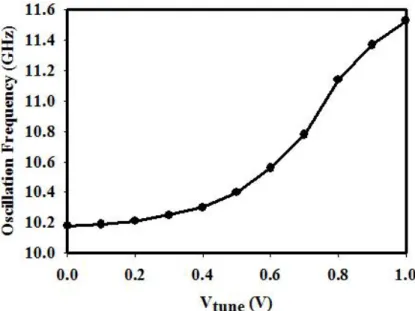
Fig. 4. Measured free-running frequency tuning range of the proposed divide-by-3
ILFD circuit. VDD=0.7V, Vg=0.5V and Vbias=0.7V.is applied to one port of the first mixer, and the output of the second mixer is fed back to the other input port of the first mixer through a filter. The input/output frequency relation is given by ω
RF− 2ω
o=ω
ofor the divide-by-3 function. Using this approach might lead to a large locking range because of linear mixer. The use of two mixers can increase the dc power so the second mixer is stacked in series on the first mixer in the proposed circuit, so that dc current can be reused and a lower power ILFD can be implemented.
4. Circuit Design
Figure 2 shows the circuit for CMOS divide-by-3 ILFD used in
this work. The circuit consists of a cross-coupled pair M
n1and M
n2,
which provide negative transconductance to compensate for the tank
loss. The sources of cross-coupled pair transistors are not connected to a common node. They are fed by another differential pair M
n3and M
n4that injects the input signal current. The transistors M
n3and M
n4also serve as mixers. The ILFD output signal at ω
ois coupled to the sources of M
n3and M
n4. The injection signal at ω
RFapplied to the gates of M
n3and M
n4mixes with the source voltage of M
n3and M
n4and generate the drain output current at ω
RF− ω
o, the drain current of M
n3and M
n4mixes with the ILFD output voltage signal through M
n1and M
n2yielding the frequency relation (ω
RF− ω
o) −ω
o=ω
o, and we can get ω
o=ω
RF/ 3. A large locking range can be obtained since the transistors M
n1and M
n2are used as a linear mixer while conventional divide-by-3 ILFD the cross-coupled transistors are used as a nonlinear second-harmonic mixer. The parallel LC branch of L
0and C
0forms a low impedance circuit at the fundamental oscillation frequency (f
o) which in effect causes the sources of cross-coupled pair M
n1and M
n2be connected together for a large loop gain and a reliable oscillation. The L
0and C
0also provide a high-impedance circuit current path at the injection signal frequency (2f
o) because their source terminals are separated. Here C
0is the capacitance at the source of M
n1or M
n2. The tail M
n5is used to optimize the power
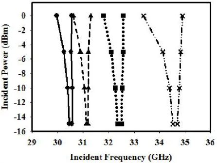
Fig. 5. Measured input sensitivity of the ILFD with 3 division ratio. V
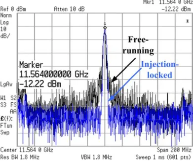
DD=0.7V, Vg=0.5V, Vbias=0.7V and Vtune=0.0, 0.5, 0.7, and 1.0 V from the left to the right.Fig. 6. Measured output spectra of the divide-by-3 ILFD before and after locking.
Fig. 7. Measured phase noises of the reference injection source and the locked ÷3
ILFD. fo=11.56GHz. Pin=0dBm. VDD=0.7V, Vg=0.5V, Vbias=0.7V, and Vtune=1.0V.consumption. An external balun T1 is used to convert a single-ended input from a signal source to differential signal. The injection signal is applied to the gate of injection MOSFET with dc gate bias V
g. In the free running operation where no injection is applied, the ILFD is a VCO with a fundamental oscillation frequency f
o. The varactors are used for frequency tuning. The voltage V
tuneis used to tune the capacitance of varactors and the oscillation frequency.
5. Measurement Results
The proposed circuit has been implemented in the retrograde
twin-well UMC 90nm 1P9M CMOS technology and the chip photo
Fig. 8. Measured input sensitivity for the circuit used as first-harmonic ILO.
VDD=0.7V, Vg=0.5V, Vbias=0.7V, and Vtune=0.0V and 1.0V from the left to the right.
of the ILFD is shown in Fig. 3, where two transformers are shown on the left and right hand sides, the small-inductor is on the top side.
The die area of the chip with is 0.81 × 0.54 mm
2. The measured tuning range is shown in Fig. 4. The tuning range of the ILFD is from 10.18 to 11.56 GHz, about 1.38 GHz (12.7%) at V
DD=0.7 V. As the gate voltage of the varactors increases, the varactor’s capacitance decreases, therefore the oscillation frequency increases.
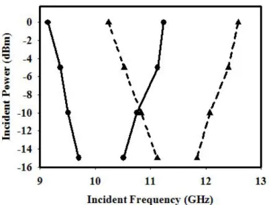
Figure 5 shows the measured relationship between input sensitivity and operating frequency of the ÷3 ILFD under the condition of incident power Pin=0 dBm, V
tune= 0.0, 0.5, 0.7 and 1.0 V and V
DD= 0.7 V, with a total operation locking range is 4.74 GHz, from 29.96 to 34.70 GHz. The ÷3 ILFD maximum locking range is about 1.53 GHz at V
tune=1.0 V, from 33.37 to 34.9 GHz. The dc bias V
gof injector’s gate is 0.5 V. The current and power consumption of the core are 2.8 mA and 1.96 mW, respectively. Figure 6 shows the measured output spectra of the ÷3 ILFD before and after the locked conditions. The locked output spectrum is sharper and shows a lower phase noise.
Figure 7 shows the measured phase noises of the injection signal
and injection-locked oscillator outputs in the ÷3 mode. At low
frequency offset, the locked phase noise is lower than the injection
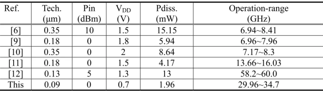
reference by around 9.5 dB. Table 1 shows the comparison between
our presented injection-locked divider and other ILFDs. Figure 8
shows the measured relationship between input sensitivity and
operating frequency for the proposed circuit used as a first-harmonic
injection-locked oscillator (ILO) under the condition of V
tune= 0.0 V,
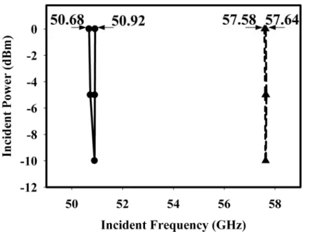
Fig. 9. Measured input sensitivity of the ILFD with 5 division ratio. V
DD=0.7V, Vg=0.5V, Vbias=0.7V, and Vtune=0.0V and 1.0V from left to right.1.0 V, and V
DD= 0.7 V, with a total locking range is 3.45 GHz, from 9.15 to 12.6 GHz. Figure 9 shows the measured relationship between input sensitivity and operating frequency for the proposed circuit used as a divide-by-5 ILFD under the condition of V
tune=0.0 V, 1.0 V and V
DD= 0.7 V, with a total locking range is 6.96 GHz, from 50.68 to 57.64 GHz. The function of 1st ILO can be described using the schematic shown in Fig. 1(b) which can not be used to describe the function of divide-by-5 ILFD. The mixers in the ÷5 ILFD are nonlinear.
6. Conclusion
This paper proposes a wide operation and wide-locking range ÷3
ILFD employing two transformers, and the injection MOSFETs are
used as mixers, in which one input signal is transformer-coupled
from the ILFD output and applied to the source and the other input
signal is applied to the gate. The ILFD circuit has been successfully
implemented in the UMC 90nm 1P9M CMOS technology and has a
good performance of lower power, and large locking range. In the
ILFD the switching transistors are used as linear mixers. The
varactor tuning is also used to extend the operation range of the
ILFD. The die area is 0.4374 mm
2. The implemented ÷3 ILFD core
consumes power of 1.96 mW at the supply voltage of 0.7V, and the
operation range is 4.74 GHz, from 29.96 to 34.70 GHz.
Table 1. Comparison of ÷3 Injection-Locked Frequency Dividers
Ref. Tech.(μm)
Pin (dBm)
VDD
(V)
Pdiss.
(mW)
Operation-range (GHz)
[6] 0.35 10 1.5 15.15 6.94~8.41
[9] 0.18 0 1.8 5.94 6.96~7.96
[10] 0.35 0 2 8.64 7.17~8.3
[11] 0.18 0 1.5 4.17 13.66~16.03
[12] 0.13 5 1.3 13 58.2~60.0
This 0.09 0 0.7 1.96 29.96~34.7
References
[1] Y.-H. Chuang, S.-H. Lee, R.-H. Yen, S.-L. Jang, J.-F. Lee, and M.-H. Juang, “A wide locking range and low voltage CMOS direct injection- locked frequency divider,” IEEE Microw. Wireless Compon. Lett., vol. 16, no. 5, pp. 299–301, May 2006.
[2] S.-L. Jang and C.-F. Lee, “A wide locking range LC-tank injection locked frequency divider,” IEEE Microw. Wireless Compon. Lett., vol. 17, no. 8, pp.
613–615, Aug., 2007.
[3] K. Yamamoto and M. Fujishim, “70 GHz CMOS harmonic injection locked divider,” In IEEE Int. Solid-State Circuits Conf. Dig., Feb. 2006, pp. 2472–2481.
[4] S.-H. Lee, S.-L. Jang, C.-F. Lee, and M.-H. Juang, “Wide locking range divide-by-4 injection locked frequency dividers,” Microwave and Optical
Technology Lett., vol. 49, no. 7, pp. 1533–1536, Jul. 2007.
[5] H. Wu and L. Zhang, “A 16-to-18GHz 0.18μm epi-CMOS divide-by-3 injection-locked frequency divider,” in IEEE ISSCC Dig. Tech. Papers, Feb. 2006, pp.27–29.
[6] S.-L. Jang, C.-Y. Lin, and C.-F. Lee, “A low voltage 0.35 μm CMOS frequency divider with the body injection technique,” IEEE Microw. Wireless Compon. Lett., vol. 18, no. 7, pp.470–472, Jul. 2008.
[7] S.-L. Jang, W. Yeh, and C.-F. Lee, “A low power CMOS divide-by-3 LC-tank injection locked frequency divider,” Microwave and Optical Technology Lett.,vol.
50, no. 1, pp. 259–262, Jan. 2008.
[8] S.-L. Jang, C.-F. Lee, and W.-H. Yeh, “A divide-by-3 injection locked frequency divider with single-ended input,” IEEE Microw. Wireless Compon. Lett., vol. 18, no. 2, pp. 142–144, Feb. 2008.
[9] S.-L. Jang, C.-C. Liu, and C.-W. Hsue, “LC-tank injection locked frequency divider with variable division ratio,” Microwave and Optical Tech. Lett., vol. 50, no. 12, pp. 3232–3236, Dec. 2008.
[10] S.-L. Jang, P.-X. Lu, C.-F. Lee, and M.-H. Juang, “Divide-by-3 LC injection locked frequency divider with a transformer as an injector’s load,” Microwave and
Optical Tech. Lett., vol. 50, no. 10, pp. 2722–2725, Oct. 2008.
[11] S.-L. Jang, R.-K. Yang, C.-W. Chang, and M.-H. Juang, “Multi-modulus LC injection-locked frequency dividers using single-ended injection,” IEEE Microw.
Wireless Compon. Lett., vol. 19, no. 5, pp. 311–313, May, 2009.
[12] T.-N. Luo, S.-Y. Bai, and Y.-J. E. Chen, “A 60-GHz 0.13-μm CMOS divide-by-three frequency divider,” IEEE Trans. Microw. Theory Tech., vol. 56, no. 11, pp. 2409–2415, Nov. 2008.
計畫編號
NSC 97-2221-E-011-138
計畫名稱 毫微米電晶體在高頻除三除頻器電路的應用性研
究(I)
出席人員姓名 服務機關及職稱
劉政辰
國立台灣科技大學電子工程研究所博士班四年級 會議時間地點 2009 年 4 月 27 日~4 月 28 日,台灣,新竹國賓飯店 27~ 30, April, 2009, Ambassador Hotel, Hsinchu, Taiwan 會議名稱 (中文)第十七屆國際電腦通訊及網路研討會
( 英 文 ) 2008 International Symposium on VLSI Design, Automation and Test (VLSI-DAT 2009)
發表論文題目 (中文)六埠三維度電感置入直接注入鎖定除頻器 (英文) Implementation of 6-Port 3D Transformer in Injection-Locked Frequency Divider
Implementation of 6-Port 3D Transformer in Injection-Locked Frequency Divider
Sheng-Lyang Jang, Senior Member, IEEE, Chia-Wei Tai, and Cheng-Chen Liu Department of Electronic Engineering. #43,Sec.4, Keelung Road.
National Taiwan University of Science and Technology, Taipei Taiwan, R.O.C.
ABSTRACT
This paper proposes a 6-port 3-dimensional (3-D) transformer used to improve the performance of injection-locked frequency divider (ILFD). The aim of the 3-D transformer is to reduce chip size and to reduce power consumption. The CMOS LC-tank ILFD is implemented using the direct injection nMOS between the differential outputs of an nMOS-core cross-coupled VCO. At the supply voltage of 0.6 V, the free-running frequency of ILFD is tunable from 4.81 GHz to 5.3 GHz. At the incident power of 0 dBm and VDD = 0.6 V, the total locking range is about 3 GHz, from the incident frequency 8.9 to 11.9 GHz for the ILFD in the divide-by-2 mode. The core power consumption is 1.02 mW. The die area is 0.394 × 0.623 mm2.
Index Terms—CMOS, stacked 3-dimensional transformer, VCO, injection-locked frequency divider, locking range.
I. INTRODUCTION
Monolithic transformers have found extensive usage in RF CMOS circuits [1-3], and they allow new circuit configurations to improve the circuit performance despite their relatively low quality (Q) factor. Planar transformers have found applications in VCO [1], LNA [2] and injection-locked frequency divider [3], etc. The application of 3-dimesnsional (3D) transformer is not extensive as that of the planar transformer, and the 3D transformer has the potential of low chip area and low production cost while it has low Q-factor. The Q-factor of a transformer is determined by the transformer’s geometry, the type of interconnect metal, thickness of the metallization, vertical and horizontal distance between the metal windings. The 3D transformer can have a lower Q-factor because it uses the metal layers with higher resistivity than the top thick metal layer.
In this paper, we propose a 6-port stacked 3D transformer to be implemented in an injection-locked frequency divider (ILFD) circuit to improve the performance of ILFD. The ILFD is an oscillator that takes a sinusoidal input signal and generates a periodic output signal at a frequency that is a fraction of the input signal. In an ILFD, low Q-factor resonator is often adopted to trade-off between the power consumption, the locking range and the output voltage swing. In well-designed ILFDs, the phase noise is primarily determined by the injection source, and a high Q-factor transformer is not necessary for a low phase noise performance, and the merit of reducing the chip area of 3D transformer can be maintained.
FIGURE 1. (a) 3-D view of the proposed transformer and (b) simplified circuit symbol.
FIGURE 2. Schematic of the implemented 3-D transformer-feedback ILFD.
The 3D transformer can be configured in a symmetric or asymmetric [4-7] topology. The proposed fully-integrated 6-port transformer consists of two symmetric stacked center-tapped inductors, it occupies small chip area and can be used to lower the supply voltage of ILFD, and hence the power consumption of chip can be reduced. The proposed low voltage ILFD is configured in the 5.0 GHz band and it has the characteristics of small area, low power, and wide locking range.
II. CIRCUIT DESIGN
Figure 1(a) shows the 3-D view of the proposed transformer using 6 metal layers and a simplified circuit symbol is shown in Fig. 1(b). The whole transformer consists of two center-tapped inductors stacked vertically. The first center-tap inductor is laid out as square spirals using 3 top metal layers and the
FIGURE 3. Chip photo. Chip size: 0.394 × 0.622 mm2.
FIGURE 4. Measured frequency tuning range of the proposed ILFD circuit. VDD = 0.6V.
second inductor is laid out with the 3, 2 and 1 metal layers. The transformer is laid out so that the secondary coil lies inside the primary coil. The metal trace-to-trace parasitic capacitance is minimized to maximize the operation frequency. Symmetric layout of the primary and secondary inductors is required for the differential operation, and it is not necessary for the primary to be symmetric with respect to the secondary. Port 1/Port2 is placed at the top metal (metal 6), Port3 is at the metal 4, while Port 4/Port5 is located in the metal 3 and Port6 is at the metal 1. The transformer is simulated by using the simulation tool-ADS Momentum and Spectre RF to get its related model parameters. The simulated Q-factor and inductance of the primary transformer at 5 GHz are about 4.762 and 1.723 nH, respectively. The Q-factor and inductance of the secondary transformer at 5 GHz are about 3.936 and 1.276 nH, respectively. The primary transformer has an inner length of 115-μm, metal width of 10-μm, and secondary transformer has an inner length of 88-μm, metal width of 10-μm. The proposed 3-D stacked transformer used 6 metal layers.
This work uses the 3D transformer to gain a low Q, so as to the ILFD has a larger locking range and reduce the chip-size. Therefore, the 3-D stacked transformer suitably is applied in ILFD.
F i g u r e 2 s h o w s t h e i m p l e m e n t e d 3 D transformer-feedback ILFD circuit, where four inductors are configured as a single transformer. The ILFD based on a nMOS cross-coupled VCO, and the transistors (M1, M2) are used to generate negative resistance to compensate for the tank loss in oder to the oscillator can sustain voltage swing at output. The transformer swings the output signals dynamically above the supply voltage and below the ground potential [1] so that a low supply voltage can be used to decrease the power consumption. An injection
FIGURE 5. Measured locking range of a division ratio of 2 ILFD versus the input power. VDD = 0.6 V
(a)
(b)
FIGURE 6(a). Measured phase noises of the reference injection source and the locked ILFD (top plot). (b) Measured locked and free running spectra of the divide-by-2 ILFD. Injected power= 0 dBm. VDD = 0.6 V(bottom plot).
mixer MOS M3 is connected between the VCO output nodes for coupling an external signal to the resonator.
Two varactors connected in back-to-back are used for frequency tuning and extending the ILFD operational locking range.
The operation principle of the circuit is as follows.
When the ILFD operates as a free-running oscillator, no injection signal is applied to the ILFD, the injection mixer M3 becomes a resonator load. The drain output voltage vds of M3 can be written as Vdscos(ωot), where ωo is the radian oscillation frequency and Vds is the amplitude of oscillation.
Upon applying an injection signal to the ILFD, the transistor M3 is used as a nonlinear mixer. The drain current iDS of FET M3 is modulated by the injection
FIGURE 7. Measured locking range of a divide-by-1 ILFD versus the input power. VDD = 0.6 V.
signal, VRFcos(ωRFt), with the frequency ωRF and voltage amplitude VRF. Using Taylor’s series expansion, the nonlinear drain current iDS.of FET M3 can be expressed as [8]
i vd( gs,vds)≅K2gm go gs ds& v v +K3gm&2go gs dsv v 2+....(1) where only the related terms for the ÷2 and ÷1 function are retained and K3gm&2go and K2gm&go are the cross-modulation coefficients. The mixing output due to the first term on the right-hand side of (1) has a low frequency (ωRF-ωo) component and the high frequency components are filtered out by the LC resonator. The input/output frequency relation is described by ωRF - ωo = ωo and a divide-by-2 function is obtained.
The mixing output due to the second term on the right-hand side of (1) has a low frequency (2ωo - ωRF) component and the high frequency components are filtered out by the LC resonator. The input/output frequency relation is described by 2ωo - ωRF = ωo, and the oscillation frequency is the same as the fundamental frequency of the injetion signal so as to a divide-by-1 function is obtained. The locking range for the divide-by-2 frequency divider has been be derived in [9], similar approach can be used for higher-order modulo dividers. According to [9], the injection current Iinj of ILFD in the lower-order modulo mode is larger than that in higher-order modulo mode, therefore the relative locking range in the divide-by-1 mode is larger than divide-by-2 mode.
III. RESULTS ANDDISCUSSION The transformer and the integrated ILFD circuit were fabricated by the TSMC 0.18μm 1P6M CMOS technology and the chip photo of the ILFD is shown in Fig. 3. The chip area is 0.394 × 0.623 mm2 including pads. The measured tuning range is shown in Fig. 4. The tuning range of the ILFD is from 4.81 GHz to 5.3 GHz, which is about 0.49 GHz (9.7%) at VDD = 0.6V. The dc bias Vinj of injector’s gate is 0.6 V.
The varactors are accumulation mode nMOS varactors.
As the gate voltage of the varactors increases, the varactor’s capacitance decreases, and the oscillation frequency increases. Figure 5 shows the measured relationship between locking range and input power of the ILFD with a division ratio of 2 under the condition of vtune =0.0, 0.5 and 1.0 V at VDD = 0.6 V. The total locking range is from 8.9 GHz to 11.9 GHz (28.8%).
The core power consumption is 1.02mW. Figure 6(a) shows the measured phase noises of the injection
TABLE I
Performance Comparison of Divide-by-2 ILFD.
VDD
* Pin: injection power
signal and injection-locked oscillator outputs in the ÷2 mode. The phase noise of injection reference at 1MHz offset from thefrequency 5.0 GHz is about -126.4 dBc/Hz. After external power injection at 0 dBm, the ILFD phase noise is about -126.5 dBc/Hz at 1MHz offset from the frequency 5.0 GHz in the ÷2 mode.
The phase noise of locked ÷2 ILFD is lower than that of the injection reference at low frequency. Figure 6(b) shows the measured output spectra of the divider before and after the locked conditions in the ÷2 mode.
The locked spectrum shows a lower phase noise.
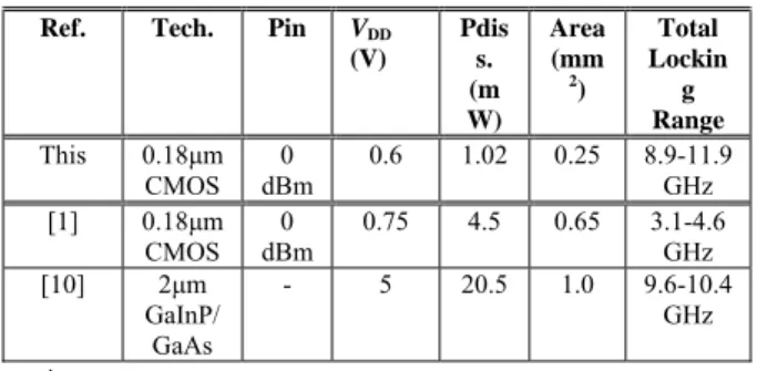
Figure 7 shows the measured locking range of the ILFD in the ÷1 mode under the condition of vtune = 0.0, 0.5 and 1.0 V, and VDD = 0.6 V, with a total locking range from 2.7 GHz to 8.2 GHz at the injection power of 0 dBm. Table I shows the comparison between our presented ILFD and previously published ILFD reports with transformers.
The ILFD has a good performance with smaller occupied chip area and lower power consumption.
IV. CONCLUSION
The paper proposes a 6-port stacked 3-D transformer used in a 5GHz ILFD, which has the properties of small die area, low voltage and low power, and a large locking range. The 3-D transformer serves two roles. One is to swing the voltage above and below the supply voltage so that low power chip can be used, and the other is to reduce chip area and product cost. The transformer and the ILFD circuit were fabricated in the 0.18μm CMOS technology, and the ILFD uses two cross-coupled transistors and the transformer to form the differential oscillator. The die area of ILFD is 0.25 mm2. The implemented ILFD core consumes 1.02 mW at the supply voltage of 0.6 V, and at 0dBm injection power the measured locking range is from the incident frequency 8.9 GHz to 11.9 GHz.
ACKNOWLEDGMENT
The authors would like to thank the Staff of the CIC for the chip fabrication and technical supports.
REFERENCES
[1] Y.-H. Chuang, S.-H. Lee, R.-H. Yen, S.-L. Jang, J.-F. Lee and M.-H. Juang, “A wide locking range and low voltage CMOS direct injection-locked frequency divider,” IEEE Microw. Wireless Compon. Lett., vol. 16, no. 5, pp. 299-301, May 2006.
Ref. Tech. Pin (V)
Pdis s.
(m W)
Area (mm
2)
Total Lockin g Range This 0.18μm
CMOS 0 dBm
0.6 1.02 0.25 8.9-11.9 GHz [1] 0.18μm
CMOS 0
dBm 0.75 4.5 0.65 3.1-4.6 GHz [10] 2μm
GaInP/
GaAs
- 5 20.5 1.0 9.6-10.4 GHz
[2] J.J. Zhou and D.J. Allstot, “Monolithic transformers and their application in a differential CMOS RF low-noise amplifier,”
IEEE J. Solid-State Circuits, vol.33, no.12, pp.2020-2027, Dec. 1998.
[3] S.-H. Lee, S.-L. Jang, and Y.-H. Chung , “A low voltage divide-by-4 injection locked frequency divider with quadrature outputs,” IEEE Microw.
Wireless Compon. Lett., vol. 17, no. 5, pp.373-375, May, 2007.
[4] J. R. Long, “Monolithic transformers for silicon RF IC design,” IEEE J. Solid-State Circuits, vol.35, no.9, pp.1368-1382, Sep. 2000.
[5] A. Zolfaghari, A. Chan, and B. Razavi, “Stacked inductors and transformers in CMOS technology,” IEEE J. Solid-State Circuits. vol.36.
no. 4, pp.620-628, Apr. 2001.
[6] W.-Z. Chen and K.-C. Hsu, “Miniaturized 3-dimensional transformer design,” in Proc.
IEEE Custom Integrated Circuit Conf., pp.
285-288, Sep. 2005.
[7] W.-Z. Chen and W.-H. Chen, “Symmetric 3D passive components for RF ICs application,” in Proc. IEEE Radio Frequency Integrated Circuits Symp., pp. 599-602, Jun. 2003.
[8] P. Wambacq and W. Sansen, Distortion Analysis of Analog Integrated Circuits, Norwell, MA:
Kluwer, 1998.
[9] B. Razavi, “A study of injection locking and pulling in oscillators,” IEEE J. Solid-State Circuits, vol. 39, no. 9, pp. 1415-1424, Sep.
2004.
[10] H.-J.Wei, C. Meng, Y. Chang, and G.-W. Huang,
“Injection-Locked GaInP/GaAs HBT Frequency Divider with stacked transformers,” Microw. and Optical tech. Lett., vol. 49, no. 10, Oct. 2007.