sistors with Au and Ti/Au metal gates are comprehensively studied and demonstrated. By evaporating the Ti/Au metal gate, the thermal stability of device characteristics are significantly improved as compared with the device with conventional metal gate 共Au兲. Experimentally, the device with a Ti/Au metal gate simultaneously exhibits the considerably lower temperature degradation in turn-on voltage 共−2.19 mV/K兲, breakdown voltage 共−34 mV/K兲, logic swing 共−1.24 mV/K兲, transition region width 共0.05 mV/K兲, on-off current ratio 共−3.55 /K兲, threshold voltage 共−0.25 mV/K兲, impact ionization-induced gate current 共1.63
⫻ 10−3A/mm K兲, output conductance 共1.23 S/mm K兲, and voltage gain 共−0.33 /K兲 as the temperature is increased from 300 to 510 K. Consequently, the studied device with a Ti/Au metal gate is a good candidate for high-speed and high-temperature digital and switching circuit applications.
© 2007 The Electrochemical Society. 关DOI: 10.1149/1.2430649兴 All rights reserved.
Manuscript received September 20, 2006; revised manuscript received October 30, 2006.
Available electronically January 18, 2007.
Recently, metamorphic heterostructure field-effect transistors 共MHFETs兲 have received much attention for high-performance inte- grated electronic circuit applications.1,2As compared with InP-based transistors,3,4 the metamorphic structure offers several advantages such as low cost, less fragility, large substrate size, high crystal quality, and mature back-side processing. In addition, the metamor- phic structures give a free choice of lattice constant and indium composition of InxGa1−xAs channel. However, the high In mole frac- tion of InGaAs channel used in MHFET is observed to easily initiate the impact ionizations.5If the electric field is high enough to accel- erate carriers within the channel, the electron gains kinetic energy to collide with the lattice and generate electron-hole pairs.6Some holes injected across the Schottky layer and trapped close to the gate terminal could lead to a negative shift of the threshold voltage.
Subsequently, through the degraded gate control ability as well as reduced gate depletion region, the kink effect and bell-shaped be- havior occur.2,7 Therefore, the deposition of mechanically stable metal gates has become a critical issue. In particular, the require- ments of a thermally stable Schottky gate contact are that the metal gates can survive during high-temperature process and device opera- tion. Because the frequently used Pt metal is easy to chemically react with GaAs or AlGaAs layer and forms compounds at relatively low temperature,8it may be unsuitable for application in the gate electrode of metal semiconductor field-effect transistors.
In this work, the double ␦-doped In0.42Al0.58As/In0.46Ga0.54As MHFETs with different metal gates, e.g., Ti/Au and Au, are fabri- cated to comprehensively study their thermal stability performance over a wide temperature range共300–510 K兲. Also, to study the elec- trical properties in digital and switching circuit applications, the voltage transfer characteristics are included. The temperature degra- dation rates in device characteristics depend strongly on the specific metal gates. By the employment of Ti as a part of metal gate, the lower deviation and higher performance of Schottky gate contacts are obtained even at high ambient temperature. This also implies that the impact ionizations and related thermal runaway are sup- pressed. Therefore, the higher temperature operation capability and relatively thermal stability are simultaneously enhanced in device operations.
Experimental
The studied double ␦-doped In0.42Al0.58As/In0.46Ga0.54As MHFET, grown by molecular beam epitaxy, consisted of buffer, active, barrier, and cap structures. The buffer structure, including a 1.5m thick linearly graded InAlAs metamorphic layer and a 300 nm In0.42Al0.58As layer, was deposited on the semi-insulating GaAs substrate. Upon the buffer structure, the active structure in- cluded a silicon planar doping layer of␦2共n+兲 = 2 ⫻ 1012cm−2, a 5 nm In0.42Al0.58As space layer, a 20 nm In0.46Ga0.54As channel layer, a 5 nm In0.42Al0.58As space layer, and a silicon planar doping layer ␦1共n+兲 = 4 ⫻ 1012cm−2. The barrier structure was a 30 nm In0.42Al0.58As layer. The cap structure was a 5 nm n+ -In0.43Ga0.57As共n+= 5⫻ 1018cm−3兲 layer. The Hall measurement showed the sheet carrier density共ns兲 of 4.1 ⫻ 1012cm−2and elec- tron mobility共n兲 of 8100 cm2/V s at room temperature. The stud- ied devices were fabricated in the following sequences. Standard photolithography, hard backing, and wet chemical etching were em- ployed for device isolation. AuGeNi metals were evaporated on cap structure and annealed by rapid thermal annealing to from drain- source ohmic contacts. The cap structure was selectively etched over the barrier structure by using the pH-adjusted succinic acid solution 共HOOCCH2CH2COOH, H2O2, and NH4OH兲. After the etching pro- cess, the separate metals of Ti/Au 共device A兲 and Au 共device B兲 were deposited on the barrier structure, respectively, to the Schottky gate contact. Finally, the barrier and active structures underneath the gate feeder were completely removed by wet chemical etching to build the air-bridge gate structure.9For the conventional mesa-type devices, the gate-feeder metal lying on the mesa sidewall of the narrow-gap channel caused the higher gate leakage current, addi- tional parasitic capacitance, and impact ionization effect. However, by using the air-bridge type devices in this work, these undesirable problems can be effectively reduced and eliminated. The schematic cross sections of the studied devices are depicted in Fig. 1. An HP4156A semiconductor parameter analyzer was used to measure the experimental dc characteristics at different temperature. To com- pare and evaluate the thermal stability performance of different Schottky gate contacts, the temperature-dependent characteristics for devices A and B were investigated.
Results and Discussion
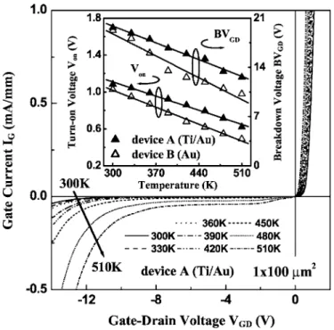
The gate-drain I-V characteristics of device A at different tem- perature are shown in Fig. 2. The inset shows the temperature de-
zFax:⫹886-6-209-4786; E-mail: [email protected]
pendences of turn-on voltage共Von兲 and breakdown voltage 共BVGD兲.
The Vonand BVGDare measured under the gate current of 1 and
−0.5 mA/mm, respectively. For device A共with a Ti/Au metal gate兲, the temperature degradation rates in Von 共Von/T兲 and BVGD
共BVGD/T兲 are only of −2.19 and −34 mV/K, respectively, as the temperature is increased from 300 to 510 K. The corresponding temperature degradation rates of device B共with a Au metal gate兲 are
−2.62 and −44.5 mV/K, respectively. Obviously, within the tem- perature range of 300–510 K, the thermal-stable turn-on and break- down characteristics are achieved for device A. This is attributed to the reduced tunneling mechanism and improved Schottky perfor- mance. In other words, because Ti has a lower diffusivity and higher melting point,10it acts as a diffusion barrier to suppress the gate leakage current and related impact ionization effects with increasing temperature. Therefore, the studied device with a Ti/Au metal gate exhibits the superior performance of Schottky gate contacts.
Figure 3 shows the common-source I-V characteristics of the studied devices at different temperatures. The applied gate-source voltage VGSis −0.5 V/step. It is known that, as the temperature is increased, the increase of background carrier concentration and low- ering effect of Schottky barrier height give rise to the additional leakage paths through barrier structure.11 However, the degraded
pinch-off and saturation characteristics associated with poor carrier confinement caused by the increase of temperature are relatively insignificant for the device A. This is because the barrier metal gate of Ti is effective to improve the gate mechanical stability and pre- vent the destruction of electrical performance through Au metal diffusion.10,12Furthermore, the deviation of drain saturation current 共IDS兲 for device A is lower than that of device B. This is also caused by the improved Schottky performance presented at the Ti/Au -InAlAs Schottky gate contact. Thus, the temperature-independent characteristics of output current are obtained for device A. The static analysis of the voltage transfer characteristics is performed graphi- cally by constructing and superimposing the load line on ID-VDS curves in Fig. 3. The voltage transfer characteristics of the studied devices at different temperatures are shown in Fig. 4. The upper inset shows the studied MHFET with a resistive load. The supply voltage and load resistance are fixed at VDD= 3.5 V and RD
= 60⍀. The input and output voltages, i.e., VIL, VIH, VOL, and VOH, for logic low and high states are determined from the pairs of output voltage共Vo兲 and input voltage 共Vi兲 by using the slope criterion of dVo/dVi= −1, as shown in the lower inset in Fig. 4. Clearly, by using the refractory metal of Ti, the device A shows superior thermal Figure 1. Schematic cross sections of the studied MHFETs.
Figure 2. Gate-drain I-V characteristics of the device A at different tempera- tures. The temperature dependences of turn-on voltage共Von兲 and breakdown voltage共BVGD兲 are shown in the inset.
Figure 3. Common-source I-V characteristics at different temperatures.
Figure 4. Voltage transfer characteristics at different temperatures. The MHFET with a resistive load is shown in the upper inset. The corresponding diagram of voltage transfer characteristics is shown in the lower inset.
stability of voltage transfer curves among the temperature of 300–510 K. To further investigate the electronic parameters of logic operation, the logic swing 共Vls= VOH− VOL兲, transition region width共Vtw= VIH− VIL兲, and operation point 共VQ兲 as a function of temperature are shown in Fig. 5 and 6. Also, the VQis obtained from the intersection between the load line and IDS vs VDScurve mea- sured under different gate-source voltage 共VGS兲. Note that device with large logic swing and small transition width can reduce the ambiguity in the logic state and enhance the noise immunity.13Due to the improved thermal stability of Ti/Au-InAlAs Schottky gate contact, the device A shows higher Vls, lower Vtw, and lower degra- dation rates in Vls and Vtw 共Vls/T = −1.24 mV/K and Vtw/T
= 0.05 mV/K兲 over the temperature range between 300 and 510 K.
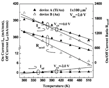
As a result, even though the temperature is elevated up to 510 K, the device A still maintains higher Vlsand lower Vtw共1.88 and 1.46 V兲 than those of device B共1.83 and 1.52 V兲. Furthermore, as compared with device B, the considerably lower deviations of operation points VQfor device A, measured at VGS= + 0.0, −0.5, and −1.0 V, are found as shown in Fig. 6. Thus, the VQor dc biasing of device A is more stabilized against variations in temperature. The on current 共Ion兲, off current 共Ioff兲, and on-off current ratio 共Ron-off= Ion/Ioff兲 as a function of temperature are shown in Fig. 7. The biased voltage is fixed at VDS= + 2.0 V. For devices A and B, the temperature deg-
radation rates in Ion 共Ion/T兲, measured at VGS= + 0.0 V, are
−0.18 and −0.25 mA/mm K as the temperature is increased from 300 to 510 K. The corresponding temperature degradation rates in Ioff 共Ioff/T兲, measured at VGS= −2.0 V, are 1.72 and 18.5A/mm K. Experimentally, the device A exhibits higher Ron-off
values than device B. For instance, the Ron-offvalue of device B共70兲 is about 7 times in magnitude lower than that of device A共529兲 at 510 K. In addition, the associated temperature degradation rates in Ron-off, i.e.,Ron-off/T, are −3.55 and −6.22 /K for devices A and B, respectively. Due to the large power dissipation and low thermal conductivity of GaAs substrate at higher temperature, the device operating temperature is raised and much higher than the ambient temperature.14 Therefore, once the temperature is increased from 300 to 510 K, the annealing effect and performance degradation may be observed more easily in device B. This is caused by the interdiffusions between the Au metal and the barrier structure at higher temperature.15However, for device A, the Ron-offvalues are remarkably improved over the measured temperature range. This indicates that the studied device with a Ti/Au metal gate is certainly suitable for high-temperature digital and switching circuit applica- tions.
The threshold voltage共Vth兲 and variation of Vth共⌬Vth兲 as a func- tion of temperature are illustrated in Fig. 8. The biased voltage is fixed at VDS= 2.0 V. For device A共B兲, the variation magnitude of Vthand degradation rates of Vth, i.e., 兩⌬Vth兩 andVth/T, are 50.2 共81.5兲 mV and −1.98 共−2.05兲 mV/K, respectively, over a wide tem- perature ranging from 300 to 510 K. As the temperature is elevated, the considerable thermionic emission leakage current of device B is injected from the gate terminal into the active structure. Subse- quently, a higher兩VGS兩 is needed to extend the gate depletion region and then the magnitude of Vthof device B is increased more rapidly.
However, for device A, the increase of leakage current and decrease of⌽B, caused by the increase of temperature, are indeed suppressed.
This indicates that the superior rectifying performance as well as gate control ability are obtained for the studied device with a Ti/Au metal gate.
According to the excess gate hole current model established by Webster et al.,16 the impact ionization-induced gate current共IG,ii兲 can be expressed as
IG,ii= IG− IG,Schottky 关1兴
where IG is the total gate current and IG,Schottky the Schottky gate leakage current. The IG,ii vs gate-source voltage 共VGS兲 at different Figure 5. Logic swing共Vls兲 and transition region width 共Vtw兲 as a function
of temperature.
Figure 6. Operation point共VQ兲 as a function of temperature under different gate-source voltage共VGS兲.
Figure 7. On current共Ion兲, off current 共Ioff兲, and on-off current ratio 共Ron-off兲 as a function of temperature.
temperatures is shown in Fig. 9. The biased voltage is fixed at VDS= 2.0 V. Apparently, the IG,iishows a “bell-shaped” behavior as a function of VGS. This behavior in MHFET’s operation is due to the collection of holes generated by impact ionization which occurs in the conditions of both high electron concentration and high electric field.2,6By discriminating the following various VGSsteps, this bell- shaped behavior can be described. First, from the pinch-off condi- tion, the increase of兩IG,ii兩 under the −1.8 V ⬍ VGS⬍ −0.6 V re- gimes is caused by the increase of electron concentration in the channel as the VGS is increased. Also, with the high electric field presented in gate-drain region at high VDS bias, it contributes the enhancement of impact ionization. In contrast, the decrease of兩IG,ii兩 for VGS⬎ −0.6 V can be ascribed to the 共i兲 decrease of electric field and共ii兲 real-space transfer of electrons to the high bandgap layer as the VGS shifts toward more positive bias regime.17 This leads to the suppression of impact ionization. Besides, it is found that the bell-shaped behavior is relatively suppressed for device A.
For instance, the peak IG,ii of device A共−0.36 A/mm兲 is lower than that of device B共−0.61 A/mm兲. Because the impact ioniza- tion is dominated by the drain current density under the identical electric field, the lower drain current density of device A results in the decrease of peak IG,ii. The temperature dependences of impact ionization mechanisms in MHFET’s operation are dominated by the alternative of ionization threshold energy and hot electron
population.18With increasing temperature, the electron mobility is significantly decreased due to increased phonon scattering and re- lated reduced mean-free paths of electrons.19 This indicates that electrons cannot gain enough energy to release the lattice electrons.
Thus, the hot electron population and the corresponding impact ion- ization are substantially suppressed. As shown in Fig. 9, because the impact ionization is dominated by the ionization threshold energy, the IG,iiis decreased when the temperature is increased from 300 to 510 K. Especially, the temperature degradation rate in peak IG,ii, i.e.,
IG,ii/T, of device A 共1.63 ⫻ 10−3A/mm K兲 is improved as compared with that of device B共2.53 ⫻ 10−3A/mm K兲. This is caused by the effectively reduced impact ionization which leads to the improved thermal-stable characteristics of device A within the temperature range of 300–510 K.
Figure 10 shows the transconductance共gm兲, output conductance 共gds兲, and voltage gain 共AV兲 as a function of temperature. The biased voltages are fixed at VDS= 2.0 V and VGS= −0.8 V. The tempera- ture degradation rates in gm, gds, and AV, i.e.,gm/T, gds/T, and
AV/T, of device A 共B兲 are −0.11 共−0.21兲 mS/mm K, 1.23 共20.2兲 S/mm K, and −0.33 共−0.46兲/K, respectively. Obviously, the degraded amplification performance of device A is relatively insensitive to the increase of temperature.This indicates that the gate control ability as well as thermal stability of device A is indeed improved under various temperatures. Thus, for the studied device with a Ti/Au metal gate, good properties of amplification perfor- mance are achieved even when the temperature is elevated up to 510 K.
Conclusion
The double␦-doped In0.42Al0.58As/In0.46Ga0.54As MHFETs with Au and Ti/Au metal gates have been systematically compared and studied. The temperature-independent characteristics of the studied device were obtained by using the Ti/Au metal gate. Experimen- tally, for a 1⫻ 100 m2gate-dimension MHFET with the Ti/Au metal gate, the higher logic swing of 1.88 V, lower transition region width of 1.46 V, and higher on-off current ratio of 529 were ob- tained, respectively, at 510 K. In particular, the device with a Ti/Au meal gate showed the thermally stable performance in turn-on volt- age, breakdown voltage, logic swing, transition region width, opera- tion point, on-off current ratio, threshold voltage, impact ionization- induced gate current, output conductance, and voltage gain over a wide operating temperature range共from 300 to 510 K兲. Based on Figure 8. Threshold voltage共Vth兲 and variation of Vth共⌬Vth兲 as a function of
temperature.
Figure 9. Impact ionization-induced gate current共IG,ii兲 vs gate-source volt- age共VGS兲 at different temperatures.
Figure 10. Transconductance共gm兲, output conductance 共gds兲, and voltage gain共AV兲 as a function of temperature.
1. K. W. Lee, N. Y. Yang, M. P. Houng, Y. H. Wang, and P. W. Sze, Appl. Phys. Lett., 87, 263501共2005兲.
2. M. K. Hsu, H. R. Chen, S. Y. Chiou, W. T. Chen, G. H. Chen, Y. C. Chang, and W.
S. Lour, Appl. Phys. Lett., 89, 033509共2006兲.
3. J. S. Su, W. C. Hsu, D. T. Lin, W. Lin, H. P. Shaio, Y. S. Lin, J. Z. Huang, and P.
J. Chou, IEEE Electron Device Lett., 32, 2095共1996兲.
4. Y. S. Lin and J. H. Huang, J. Electrochem. Soc., 152, G627共2005兲.
5. M. H. Somerville, A. Ernst, and J. A. Del Alamo, IEEE Trans. Electron Devices, 47, 922共2000兲.
Symposium, 110共1991兲.
15. A. K. Sinha and J. M. Poate, Appl. Phys. Lett., 23, 666共1973兲.
16. R. T. Webster, W. Shangli, and A. F. M. Anwar, IEEE Electron Device Lett., 21, 193共2000兲.
17. E. Zanoni, M. Manfredi, S. Bigliardi, A. Paccagnella, P. Pisoni, C. Tedesco, and C.
Canali, IEEE Trans. Electron Devices, 39, 1849共1992兲.
18. C. H. Tan, G. J. Rees, P. A. Houston, J. S. Ng, W. K. Ng, and J. P. R. David, Appl.
Phys. Lett., 84, 2322共2004兲.
19. G. A. Baraff, Phys. Rev., 128, 2507共1962兲.