Improved Temperature-Dependent Characteristics of a Sulfur-Passivated AlGaAs/InGaAs/GaAs Pseudomorphic High-Electron-Mobility Transistor
Po-Hsien Lai, Ssu-I Fu, Yan-Ying Tsai, Ching-Wen Hung, Chih-Hung Yen, Hung-Ming Chuang, and Wen-Chau Liu z
Institute of Microelectronics, Department of Electrical Engineering, National Cheng-Kung University, Tainan, 70101, Taiwan
The temperature-dependent characteristics of 共NH
4兲
2S
x-passivated AlGaAs/InGaAs/GaAs pseudomorphic high electron mobility transistors were studied and demonstrated. Due to the use of sulfur passivation, remarkable improvements in device performance, including higher forward turn-on voltage, higher reverse breakdown voltage, lower reverse leakage current, higher transconduc- tance, lower on-resistance, more linear operating regime, and superior microwave performance, were obtained. In addition, the sulfur-passivated devices also show good properties in the higher operating temperature regime and relatively thermally stable performance over the operation temperature range 300–510 K. Therefore, the studied device with 共NH
4兲
2S
xtreatment provides promise for high-performance digital and microwave device applications.
© 2006 The Electrochemical Society. 关DOI: 10.1149/1.2199433兴 All rights reserved.
Manuscript submitted February 23, 2006; revised manuscript received March 16, 2006. Available electronically May 10, 2006.
Due to progressive improvements in growth techniques, hetero- structure field-effect transistors 共HFETs兲 have been studied exten- sively for high-speed microwave applications. 1-3 Nevertheless, the III-V HFETs may suffer from surface-related mechanisms. The sur- face of III-V semiconductor materials such as AlGaAs is known to be plagued by a high density of interface states. 4 Furthermore, the extrinsic surface, formed by the typical gate-recess etching pro- cesses, traps a significant portion of the electrons and causes the increase of the depletion layer between the source and the gate edge near the source. 5,6 This adversely influences the effect of applied gate bias on the active channel and results in reduced transconduc- tance and poor long-term device stability. Therefore, the lack of an adequate surface passivation for the III-V HFETs severely degrades device performance and restricts application of compound semicon- ductor circuits. In order to overcome this undesirable problem, the surface passivation becomes a crucial requirement for fabricating high-performance electronic and optoelectronic devices. 7-9 In par- ticular, sulfur passivation in a wet chemical solution of 共NH 4 兲 2 S
xwas shown to be an effective way to substantially lower AlGaAs surface recombination centers. 10,11
In this work, the temperature-dependent characteristics of a sulfur-passivated AlGaAs/InGaAs/GaAs pseudomorphic high- electron-mobility transistor 共PHEMT兲 were studied and demon- strated. Sulfur passivation was employed to a gate junction to avoid the difficulty in fabricating high-performance metal/AlGaAs Schottky contacts. The passivation method controls defective states originating from 共i兲 air oxidation of the AlGaAs surface before Schottky metallization and 共ii兲 interfacial reaction during metalliza- tion. In other words, the sulfur passivation effectively reduces the series resistances and interface states. This also indicates that the Fermi-level pinning effect produced by native surface oxides and nonradiative recombination centers can be eliminated. 11,12 There- fore, good device performance, high-temperature operation capabil- ity, and relatively thermally stable characteristics are simultaneously obtained.
Experimental
The epitaxial structure of the studied device was grown on a 共100兲-oriented semi-insulating 共S.I.兲 GaAs substrate by a metallor- ganic chemical vapor deposition 共MOCVD兲 system. The layer structure consisted of a 4000 Å GaAs buffer layer, a 200 Å AlAs buffer layer, a 50 Å Al 0.25 Ga 0.75 As space layer, a ␦-doped sheet ␦ 2 共n + 兲 = 1 ⫻ 10 12 cm −2 , a 50 Å Al 0.25 Ga 0.75 As space layer, a
150 Å In 0.15 Ga 0.85 As channel layer, a 50 Å Al 0.25 Ga 0.75 As space layer, a ␦-doped sheet ␦ 1 共n + 兲 = 4 ⫻ 10 12 cm −2 , a 400 Å n-Al 0.25 Ga 0.75 As 共n = 3 ⫻ 10 17 cm −3 兲 Schottky barrier layer, a 300 Å n-GaAs 共n = 3 ⫻ 10 17 cm −3 兲 space layer, and a 500 Å n + -GaAs 共n + 艌 3 ⫻ 10 18 cm −3 兲 cap layer. After epitaxial growth, wet chemical etching, conventional vacuum evaporation, and lift-off techniques were used to fabricate mesa-type devices. Drain-source ohmic contacts were formed on the n + -GaAs cap layer by alloying evaporated AuGeNi/Au metals at 430°C for 3 min. Then n + -GaAs cap and n-GaAs space layers were removed and the sample 共device A 兲 was immediately passivated by soaking in the ammonia–sulfide 关共NH 4 兲 2 S
x, 5% 兴 solution for 10 min at room temperature. After sur- face passivation, the sample was rinsed in deionized 共DI兲 water, followed by blown-dry N 2 gas. This procedure was used to remove thin, whitish residual amorphous sulfur on the surfaces of AlGaAs and ohmic contact metal. For comparison, another device 共denoted device B 兲 prepared with the same process only without 共NH 4 兲 2 S
xtreatment was also included in this work. Finally, the gate Schottky contacts were achieved by evaporating Pt/Au metals on the n-Al 0.25 Ga 0.75 As Schottky barrier layer with the gate dimension of 1 ⫻ 100 m 2 . The experimental dc current–voltage 共I–V兲 charac- teristics were measured by an HP4156A semiconductor parameter analyzer. The microwave performances of the studied devices were measured by an HP8510C network analyzer in conjunction with Cascade probes at different temperature. During the process, device characteristics are monitored systematically to assure that the pro- cess is reproducible.
Results and Discussion
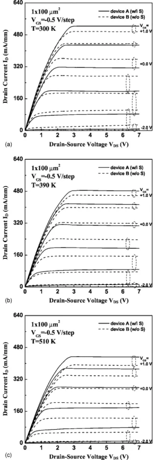
Figure 1 shows forward turn-on voltage 共V on 兲, gate-drain break- down voltage 共BV GD 兲, and reverse gate leakage current 共I
G兲 as a function of temperature. The V on , BV GD , and I
Gwere measured un- der the gate current of 1 mA/mm, −0.5 mA/mm, and the gate-drain voltage of V GD = −22 V, respectively. For device A 共with sulfur passivation 兲 and B 共without sulfur passivation兲, the V on values were decreased from 0.994 to 0.69 V and 0.936 to 0.598 V, respectively, as the temperature was increased from 300 to 510 K. The corre- sponding BV GD were decreased from 36.4 to 21.5 V and 32.4 to 16.9 V, while the corresponding I
Gvalues were increased from 0.6 to 571 A/mm and 7 to 1830 A/mm. The I
Gof device B, was several times higher than that of device A. This indicates that the high density defects were produced near the AlGaAs interface of device B, which caused the increases of nonradiative recombination centers and surface leakage current. Thus, the Schottky and break- down characteristics deteriorated. The properties of V on , BV GD , and
z