行政院國家科學委員會專題研究計畫成果報告
利用調制光譜與表面光電壓量測技術研究半導體元件結構與微細構造之光學特性(2/2) Characterization of Semiconductor Microstructures and Device Structures by using
Modulation and Surface Photovoltage Spectroscopy 計畫編號:NSC 90-2215-E-011-006
執行期限:90 年 08 月 01 日至 91 年 07 月 31 日 主持人:黃鶯聲 國立台灣科技大學電子系
共同主持人:何清華 國立東華大學材料系
計畫參與人員:梁建興,王生道,謝昌勳,陳自雄,黃鵬仁,霍克孝,周裕煥,吳政恩 台灣科技大學電子系研究生
1、中文摘要
本計劃利用各種不同之光學調制量測技 術及表面光電壓量測技術等,來研究半導 體及半導體細微結構之光學特性。此外也 探討新型結構之半導體元件之光學特性,
如、綠色雷射二極體、高速電子移動率電 晶體、異質接面雙極性電晶體、垂直面射 型雷射等的光學特性,比較各種不同調制 方式的譜線以分析調制機制。配合理論計 算,探討半導體臨界點間躍遷現象,以瞭 解其微細結構和合金成份,並分析可能影 響的因素;分析譜線的半寬度,以鑑定其 界面品質及特性,並分析可能影響的因 素。同時將研究其隨溫度和電場的變化情 形,以充掌握各種外加參數對元件品質及 性能之影響,進而提昇元件的性能。
關鍵詞:調制光譜,表面光電壓,排序,寬能 隙半導體,高速電子遷移率電晶體,異質 接面雙極性電晶體,量子井雷射,垂直面 射型雷射。
Abstr act
Modulation spectroscopy and surface photovoltage spectroscopy (SPS) are powerful techniques for studying and characterizing the properties of bulk semiconductors, reduced dimensional systems, and actual device structures. We propose a detailed study of semiconductors including wide bandgap semiconductors
(SiC
x
Ny
, GaN, BeZnSe), ordering systems (GaInP and AlGaP), semiconductor microstructures and actual device structures such as high electron mobility transistors (HEMT), heterojunction bipolar transistors (HBT), quantum well lasers (edge-emission and vertical-cavity surface-emitting laser (VCSEL) structures) by using various modulation techniques including electric field modulation, piezomodulation and photomodulation as well as SPS.The detailed study of the temperature evolution and electric field dependent of the optical transitions will be carried out. The sharp, derivative like features will be fit and the origins of the various spectral features will be identified by comparison with the theoretical calculation. The room temperature determination of the two-dimensional electron gas density for pseudomorphic GaAlAs/InGaAs/GaAs HEMT and the built fields/doping levels in the emitter and collector region of HBT will be carried out by nondestructive, contactless techniques such as photoreflectance and contactless electroflectance. In addition, the SPS will be used for characterization of the device structures such as HBT, VCSEL and edge emission laser.
Keywor ds: Modulation Spectroscopy, Surface Photovoltage Spectroscopy, Ordering, Wide Band Gap Semiconductor, High Electron Mobility Transistors, Heterojunction Bipolar Transistors, Quantum Well Lasers, Vertical-Cavity Surface-Emitting Laser
二、計畫緣由與目的
我們知道元件性能的提升,主要是歸因於 材 料 科 技 的 進 步 , 能 帶 工 程 (band engineering)進一步拓寬了元件結構設計的 空間。本計畫利用不同調制光譜及表面光 電壓量測技術,探討異質接面雙極性電晶 體、垂直面射型雷射等的光學特性之光學 特性。比較不同調制方式的譜線以分析調 制機制。配合理論計算,探討半導體能帶 或激發態之躍遷情形,瞭解其微細結構及 合金成份,並探討其可能之影響因素。
三、研究方法及計畫成果自評
研究方法
本計畫利用調制光譜及表面光電壓自 動量測系統,針對 VCSEL 及 InGaAsN /GaAs 異質接面雙極性電晶體,做以下量測 及分析:
1. 利用表面光電壓技術探討 VCSEL 結構 特性,能量隨溫度變化的詳細情形。
2. 利用光子調制技術及表面光電壓技術探 討 InGaAsN /GaAs 異質接面雙極性電晶 體結構特性。
計畫成果自評:計畫執行期間本計劃執行 期間發表相關期刊論文 11 篇,如下所示,
建立表面光電壓量測系統, 建立使用波長 調制之微分表面光電壓量測系統。
1. J. S. Liang, Y. S. Huang, C. W. Tien, Y.
M. Chang, C. W. Chen, N. Y. Li, P. W. Li, and F. H. Pollak, “Surface photovoltage spectroscopy characterization of a GaAs/GaAlAs vertical cavity surface emitting laser structure: Angle dependent”, Appl. Phys. Lett. 79, 3227-3229 (2001).
2. J. S. Liang, S. D. Wang, Y. S. Huang, C.
W. Tien, Y. M. Chang, C. W. Chen, N. Y.
Li, D. Y. Lin, and F. H. Pollak, “Polarized edge-incident photovoltage spectroscopy and reflectance characterization of a GaAs/GaAlAs vertical cavity surface emitting laser structure”, Appl. Phys. Lett.
3. Y. S. Huang, L. Malikova, F. H. Pollak, J.
P. Debray, R. Hoffman, A. Amtout, and R.
A. Stall, “Surface photovoltage spectroscopy and normal-incidence reflectivity characterization of a 1.3 ìm InGaAlAs/InP vertical cavity surface emitting laser structure”, J. Appl. Phys. 91, 6203 (2002).
4. S. D. Wang, J. S. Liang, Y. S. Huang, C.
W. Tien, Y. M. Chang, C. W. Chen, N. Y.
Li, K. K. Tiong, and F. H. Pollak, “Angle dependent differential photovoltage spectroscopy for the characterization of a GaAs/GaAlAs based vertical cavity surface emitting laser structure”, J. Appl.
Phys. 92, 2350 (2002).
5. J. S. Liang, Y. S. Huang, C. W. Tien, Y.
M. Chang, C. W. Chen, N. Y. Li, P. W. Li, and F. H. Pollak, “Angle dependent surface photovoltage spectroscopy study of GaAs/GaAlAs vertical cavity surface emitting laser structures”, 43
rd
Annual Electronic Materials Conference, Notre Dame, Indiana, USA (2001).6. Y. S. Huang, J. S. Liang, S. D. Wang, L.
Malikova, F. H. Pollak, J. P. Debray, R.
Hoffman, A. Amtout, and R. A. Stall,
“Angle-dependent surface photovoltage spectroscopy study of a 1.3 ìm InGaAlAs/InP vertical cavity surface emitting laser structure”, Internal Quantum Electronics Conference, Moscow, USSR (2002).
7. Y. S. Huang, C. J. Lin, N. Y. Li and P. W.
Li, “Photoreflectance and surface photovoltage spectroscopy characterization of an InGaP/InGaAsN/GaAs
NpN double
heterojunction bipolar transistor structure“, International Workshop on The Physic and Technology of Dilute and nitrides for Optical Communications, Istanbul, Turkey (2002)8. C. J. Lin, Y. S. Huang, N.Y. Li, P.W. Li, and K. K. Tiong, "Polarized photoreflectance characterization of an InGaP/InGaAsN/GaAs NpN double heterojunction bipolar transistor structure,"
J. Appl. Phys, Vol. 90, pp. 4565-4569 (2001).
9. D. Y. Lin, Y. S. Huang, T. S. Show, K. K.
dependent contactless electroreflectance and photoluminescence study of GaAlAs/InGaAs/GaAs pseudomorphic high electron mobility transistor structures,” J. Appl. Phys., Vol. 90, pp.
6421-6427 (2001).
10. Y. T. Cheng, Y. S. Huang, D. Y. Lin, F.
H. Pollak, and K. R. Evans, "Surface photovoltage spectroscopy characterization of the GaAlAs/InGaAs/GaAs pseudomorphic high electron mobility transistor structures with varied quantum well compositional profiles,", Physica E, Vol. 14, pp. 313-322 (2002)
11. C. H. Ho, C. H. Hsieh, Y. J. Chen, Y. S.
Huang, and K. K. Tiong, “Novel electronic design for double-modulation spectroscopy of semiconductor and semiconductor microstructures,” Review of Scientific Instruments, Vol. 72, pp. 4218-4222 (2001).
四、結果與討論
本 計 畫 針 對 VCSEL 及 InGaAsN /GaAs 異質接面雙極性電晶體,以不同調制 光譜量測技術作其光學性質研究。量測不 同溫度 VCSEL 及 InGaAsN /GaAs 異質接 面雙極性電晶體之光子調制技術及表面光 電壓譜線,探討躍遷能量與溫度之關係。
光子調制技術及表面光電壓量測結果顯示 此量測技術為研究微細結構的有力工具,
可估算費米能階,二維電子密度及內建電 場等參數,為鑑定 VCSEL 及異質接面雙 極性電晶體結構的有力工具。
五、參考文獻
1. F. H. Pollak and H. Shen, Mater. Sci. Eng.
R. 10, 275(1993).
2. F. H. Pollak in: Balkanski M (ed.) Handbook on Semiconductors Vol. 2, North Holland, Amsterdam (1994).
3. F. H. Pollak in: Halevi P (ed.) Photonic Probes of Surfaces, North-Holland, New York (1995).
a. VCSEL
0.85 0.90 0.95 1.00 1.05 1.10 1.15 1.20
60
0CM 45
030
015
05
0R (a. u.)
Photon Energy (eV)
Figure 1 presents room temperature angle-dependent R spectra.
0.85 0.90 0.95 1.00 1.05 1.10 1.15 1.20 1.25 CM
QW 60
045 0 30 0 15 0 0 0
SP V (a .u. )
Photon Energy (eV)
Figure 2 presents room temperature angle-dependent SPV spectra.
0 . 8 0 0 . 8 5 0 . 9 0 0 . 9 5 1 . 0 0 1 . 0 5 1 . 1 0 1 . 1 5 1 . 2 0
( ∆V/∆E)/V DSPV SPV NIR
C M 1
0
( d ) D S P V ( c ) (∆ V / ∆ E ) / V ( b ) S P V ( a ) N I R
P h o t o n E n e r g y ( e V )
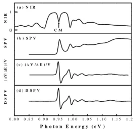
Figure 3 shows the room temperature R, SPS, numerical differential calculated SPS and DSPS measurements
0 . 8 5 0 . 9 0 0 . 9 5 1 . 0 0 1 . 0 5 1 . 1 0 1 . 1 5 1 . 2 0 1 . 2 5 E x p e r i m e n t
F i t
D S P V ( a .u .)
6 0
o3 0
o4 5
o1 5
o0
oC M B
A
x 5
P h o t o n E n e r g y ( e V )
0 .9 4 0 .9 5 0 .9 6
Figure 4 presents room temperature angle-dependent DSPV spectra.
0 1 0 2 0 3 0 4 0 5 0 6 0
0 . 9 4 0 . 9 5 0 . 9 6 0 . 9 7 0 . 9 8 0 . 9 9
Q W C M Ec a v( R ) Ec a v( S P V ) EQ W( S P V ) Ec a v( D S P S ) EQ W( D S P S )
P h o t o n E n e r g y ( e V )
A n g l e o f I n c i d e n c e ( D e g . )
Figure 5 shows the results of room temperature angle-dependent DSPS, SPS and R measurements
0 .8 5 0 .9 0 0 .9 5 1 .0 0
Q W C M 4 2 0 K
4 0 0 K 3 8 0 K
3 6 0 K 3 4 0 K
3 2 0 K 3 0 0 K θ = 0
oD S P V ( a .u )
P h o t o n E n e r g y ( e V )
0 .8 5 0 .9 0 0 .9 5 1 .0 0
Q W C M
3 4 0 K
4 2 0 K 4 0 0 K
3 8 0 K 3 6 0 K
3 2 0 K 3 0 0 K θ = 6 0
oP h o t o n E n e r g y ( e V )
Figure 6 shows representative DSPV spectra recorded at è = 0°and è = 60° with
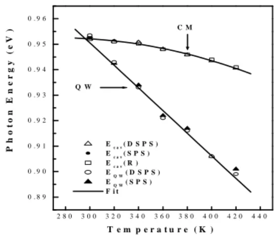
2 8 0 3 0 0 3 2 0 3 4 0 3 6 0 3 8 0 4 0 0 4 2 0 4 4 0 0 . 8 9
0 . 9 0 0 . 9 1 0 . 9 2 0 . 9 3 0 . 9 4 0 . 9 5 0 . 9 6
Q W
C M
E
c a v( D S P S ) E
c a v( S P S ) E
c a v( R ) E
Q W( D S P S ) E
Q W( S P S ) F i t
P h ot on E n e r g y ( e V )
T e m p e r a t u r e ( K )
Figure 7 shows the results of the temperature-dependent DSPS, SPS and R measurements
b. InGaAsN HBT
1.0 1.2 1.4 1.6 1.8 2.0 2.2
(b) (a)
Expt.
Fit
Collector
Base Emitter
Photon Ener gy(eV)
∆ R /R ( a . u .)
~ ~ ~ ~
0 0
_
E||[110]
E||[110]
PR 300 K
Figs. 8(a) and 8(b) are the 300 K PR spectra of the DHBT sample with electric-field vector E||[110] and E||[110], respectively
0.95 1.00 1.05 1.10 1.15 1.20 1.25 1.30 1.35 1.40
( ∆ V/ ∆ E )/ V ( a . u .)
E xpt.
F it
InG a AsN InG a As
(b)SP S
Photon Ener gy(eV)
0
0
∆ R /R ( a . u .) (a)P R 300 K
Figs. 9(a) and 9(b) are the 300 K PR and normalized first derivative surface photovoltage (SPV) spectra of the
5
行政院國家科學委員會補助專題研究計畫成果報告
※※※※※※※※※※※※※※※※※※※※※※※※※※
※ 利用調制光譜與表面光電壓量測技術研究半導體元件 ※
※ 結構與微細構造之光學特性(2/2) ※
※ Char acter ization of Semiconductor Micr ostr uctur es and Device ※
※ Str uctur es by using Modulation and Sur face Photovoltage Spectr oscopy ※
※※※※※※※※※※※※※※※※※※※※※※※※※※
計畫類別:■個別型計畫 □整合型計畫 計畫編號:NSC 90-2215-E-011-006
執行期間:90 年 08 月 01 日至 91 年 07 月 31 日
計畫主持人:黃鶯聲 國立台灣科技大學電子系 共同主持人:何清華 國立東華大學材料系
計畫參與人員:梁建興,王生道,謝昌勳,陳自雄,黃鵬仁,霍克孝, 周裕煥,吳政恩 國立台灣科技大學電子系研究生
本成果報告包括以下應繳交之附件:
□赴國外出差或研習心得報告一份
□赴大陸地區出差或研習心得報告一份
□出席國際學術會議心得報告及發表之論文各一份
□國際合作研究計畫國外研究報告書一份
執行單位:國立台灣科技大學電子系
中 華 民 國 91 年 10 月 30 日