In 0.34 Al 0.66 As 0.85 Sb 0.15 Õ ␦ „ n ¿ … -InP heterostructure field-effect transistors
Y. S. Lin, W. C. Hsu,
a)and C. Y. Yeh
Department of Electrical Engineering, National Cheng Kung University, 1 University Road, Tainan, Taiwan, Republic of China
H. M. Shieh
Department of Electronic, Kung-Shan Institute of Technology, Tainan, Taiwan, Republic of China 共Received 9 November 1999; accepted for publication 29 March 2000兲
A lattice-matched ␦ -doped In
0.34Al
0.66As
0.85Sb
0.15/InP heterostructure field-effect transistor 共HFET兲 which provides large band gap ( ⬃1.8 eV), high Schottky barrier height (
B⬎0.73 eV), and large conduction-band discontinuity ( ⌬E
c⬎0.7 eV) has been proposed. In
0.34Al
0.66As
0.85Sb
0.15/InP heterostructures are shown to be type II heterojunctions with the staggered band lineup. This HFET demonstrates a output conductance of less than 1 mS/mm. Two-terminal gate-source breakdown voltage is more than 20 V with a leakage current as low as 170 A at room temperature. High three-terminal off-state breakdown voltage as high as 36 V, and three-terminal on-state breakdown voltage as high as 18.6 V are achieved. The gate voltage swing is also significantly improved.
© 2000 American Institute of Physics. 关S0003-6951共00兲05121-4兴
InP-based modulation-doped field transistors 共MODFETs兲 have attracted much attention in microwave and optoelectronic applications, but the parallel conduction in the doped high band gap material may degrade the gate voltage swing. Consequently, the output waveform will dis- tort with respect to the input signal. The presence of higher order harmonic terms will also limit the input voltage swing and reduce the total output power. Therefore, it is interesting to investigate the linearity characteristics of microwave tran- sistors. Recently, InAlAs/InGaAs MODFETs have demon- strated superior low-noise performance over AlGaAs/GaAs MODFETs.
1Unfortunately, high output conductance and low breakdown voltage remained as the significant obstacles for high-gain and high-power microwave applications. This is basically due to two fundamental facts. First, In
0.53Ga
0.47As has a band gap (E
G) of 0.73 eV, about half the band gap of GaAs (E
G⫽1.42 eV). Second, In
0.52Al
0.48As has a lower Schottky barrier height 共0.66 eV兲 than AlGaAs 共1 eV 兲. Therefore, there is a strong interest in the development of InP-channel MODFETs
2–4for high power applications.
This is due to the inherent properties of InP such as: 共1兲 large electron saturation velocity
5and large intervalley energy gap 共0.54 eV兲,6 共2兲 low impact ionization coefficient, resulting from high breakdown fields, and 共3兲 high thermal conductivity.
7 An excellent alternative material system is lattice-matched In
0.34Al
0.66As
0.85Sb
0.15/InP due to the large band gap ( ⬃1.8 eV),8 high Schottky barrier height (
B
⬎0.73 eV) of In
0.34Al
0.66As
0.85Sb
0.15, and to the large conduction-band discontinuity ( ⌬Ec⬎0.7 eV) at the InAlAsSb/InP heterojunction. On the other hand, there are several advantages for the use of ␦ doping when compared to homogenous doping, such as high two-dimensional electron gas 共2DEG兲 concentration along with enhanced mobility, re- duced parallel conduction, and improved breakdown voltage.
However, to date, applications of ␦ -doped technique to lat-
tice matched or strained heterostructure field-effect transis- tors 共HFETs兲 are still concentrated on GaAs-based HFETs.
9,10In this letter, we propose an In
0.34Al
0.66As
0.85Sb
0.15/InP heterostructure field-effect tran- sistor using single ␦ -doped InP channel 共SD-HFET兲. Experi- mental results demonstrate that the output conductance, breakdown voltage, and linearity show significant improve- ment when compared with the previously reported InP-based devices.
2–4,11The studied single ␦ -doped In
0.34Al
0.66As
0.85Sb
0.15/InP HFET was grown by low-pressure metalorganic chemical vapor deposition 共LP-MOCVD兲 system. It consisted of a 0.5
m undoped InP buffer layer, a ␦ -doped InP channel layer, a 150 Å undoped InP spacer layer, a 400 Å undoped In
0.34Al
0.66As
0.85Sb
0.15Schottky layer, a undoped In
0.53Ga
0.47As setback layer, and finally a 200 Å n
⫹-InP cap layer sequentially grown on a 共100兲-oriented Fe-doped semi- insulating InP substrate. The growth temperature and pres- sure were 650 °C and 100 Torr, respectively. Trimethylin- dium 共TMI兲, trimethylgallium 共TMG兲, trimethylaluminum 共TMA兲, trimethylantimony 共TMSb兲, arsine (AsH3), and phosphine (PH
3) were used as the In, Ga, Al, Sb, As, and P sources, respectively. Silane (SiH
4) was adopted as the n-type source. ␦ doping is realized by the ‘‘interrupt-growth procedure,’’ i.e., by switching off In sources while keeping PH
3and silane sources flowing during the growth procedure.
The secondary-ion mass spectrometry 共SIMS兲 profiles are used to measure the dopant atom distribution. The full width at half maximum 共FWHM兲 of Si profile is 90 Å. This indi- cates that a very sharp doping profile can be achieved. Au/
Ge/Ni metal was used for source and drain ohmic contacts, onto which Ag was evaporated to further reduce the contact resistance. The gate was recessed by wet etching of n
⫹-InP and i-InGaAs using H
3PO
4:HCl ⫽4:1 and H
3PO
4:H
2O
2:H
2O ⫽6:3:100, respectively. Au was evapo- rated on the undoped InAlAsSb layer as the Schottky contact metal. The gate dimension was 1.5 ⫻125 m
2. The gate-
a兲Electronic mail: [email protected]
APPLIED PHYSICS LETTERS VOLUME 76, NUMBER 21 22 MAY 2000
3124
0003-6951/2000/76(21)/3124/3/$17.00 © 2000 American Institute of Physics
Downloaded 06 Feb 2009 to 140.116.208.55. Redistribution subject to AIP license or copyright; see http://apl.aip.org/apl/copyright.jsp
source and gate-drain spacing were 4 and 4.5 m, respec- tively.
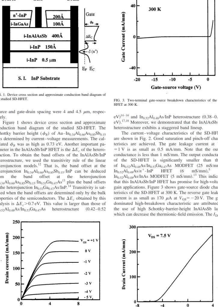
Figure 1 shows device cross section and approximate conduction band diagram of the studied SD-HFET. The Schottky barrier height (
B) of Au–In
0.34Al
0.66As
0.85Sb
0.15was determined by current–voltage measurements. The cal- culated
Bwas as high as 0.73 eV. Another important pa- rameter in the InAlAsSb/InP HFET is the ⌬Ecof the hetero- junction. To obtain the band offsets of the InAlAsSb/InP heterostructure, we used the transitivity rule of the linear heterojunction models.
12 That is, the band offset at the heterojunction In
0.34Al
0.66As
0.85Sb
0.15/InP can be deduced from the band offset at the heterojunction In
0.34Al
0.66As
0.85Sb
0.15/In
0.53Ga
0.47As
13 plus the band offsets at the heterojunction In
0.53Ga
0.47As/InP.
14Transitivity is sat- isfied when the band offsets are determined only by the bulk properties of the semiconductors. The ⌬Ec obtained by this analysis is ⌬Ec⬎0.7 eV. This value is larger than those of In
0.52Al
0.48As/In
0.53Ga
0.47As heterostructure 共0.42–0.52
obtained by this analysis is ⌬Ec⬎0.7 eV. This value is larger than those of In
0.52Al
0.48As/In
0.53Ga
0.47As heterostructure 共0.42–0.52
eV 兲14–16 and In
0.52Al
0.48As/InP heterostructure 共0.38–0.448 eV 兲.17,18Moreover, we demonstrated that the InAlAsSb/InP heterostructure exhibits a staggered band lineup.
Moreover, we demonstrated that the InAlAsSb/InP heterostructure exhibits a staggered band lineup.
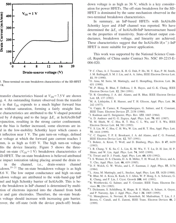
The current–voltage characteristics of the SD-HFETs are shown in Fig. 2. Good saturation and pinch-off charac- teristics are achieved. The gate leakage current at V
GS⫽1 V is as small as 0.5 mA/mm. Note that the output conductance is less than 1 mS/mm. The output conductance of the SD-HFET is significantly smaller than those of In0.52Al
0.48As/In
0.53Ga
0.47As MODFET 共25 mS/mm兲,
4
In
0.52Al
0.48As/n
⫹-InP HFET 共6 mS/mm 兲,5 and In
0.52Al
0.48As/InAs MODFET 共5 mS/mm兲.13 This indicates that this InAlAsSb/InP HFET has promise for high-voltage- gain applications. Figure 3 shows gate-source diode charac- teristics of the SD-HFET at 300 K. The reverse gate leakage current is as small as 170 A at V
GS⫽⫺20 V. The gate- dominated high-breakdown characteristic are attributed to the use of high Schottky-barrier-height InAlAsSb layer, which can decrease the thermionic-field emission. The I
DSvs
This indicates that this InAlAsSb/InP HFET has promise for high-voltage- gain applications. Figure 3 shows gate-source diode charac- teristics of the SD-HFET at 300 K. The reverse gate leakage current is as small as 170 A at V
GS⫽⫺20 V. The gate- dominated high-breakdown characteristic are attributed to the use of high Schottky-barrier-height InAlAsSb layer, which can decrease the thermionic-field emission. The I
FIG. 2. Current–voltage characteristics of SD-HFET at 300 K.
FIG. 3. Two-terminal gate-source breakdown characteristics of the SD- HFET at 300 K.
FIG. 4. IDSvs VGStransfer characteristics of the SD-HFET at 300 K.
FIG. 1. Device cross section and approximate conduction band diagram of the studied SD-HFET.
3125
Appl. Phys. Lett., Vol. 76, No. 21, 22 May 2000 Linet al.
Downloaded 06 Feb 2009 to 140.116.208.55. Redistribution subject to AIP license or copyright; see http://apl.aip.org/apl/copyright.jsp
V
GStransfer characteristics biased at V
DS⫽7.5 V are shown in Fig. 4. An outstanding feature observed from the transfer curve is that IDS expends to a much higher forward bias region without saturation, forming a fairly straight line.
These characteristics are attributed to the V-shaped potential created by ␦ doping and to the large ⌬Ec at InAlAsSb/InP heterojunction, resulting in the strong carrier confinement.
When the bias is further increased, some electrons are in- duced in the low-mobility Schottky layer which causes a slight inflection near 1 V. The gate turn-on voltage, defined as the voltage at which the forward gate current reaches 1 mA/mm, is as high as 0.85 V. The high turn-on voltage benefits the device linearity. Figure 5 shows the three- terminal on-state (V
GS⫽1 V) breakdown characteristics of the SD-HFET. The on-state breakdown is believed attributed to the impact ionization taking placing around the drain re- gion in the channel, i.e., drain-source channel breakdown.19–21The on-state breakdown voltage is as high as 18.6 V. The low output conductance and high on-state breakdown voltage are attributed to the wide-band-gap InP channel and high Schottky barrier of InAlAsSb. This is be- cause the breakdown in InP channel is determined by multi- plication of electrons injected into the channel from both source and gate electrodes. Therefore, the on-state break- down voltage should increase with increasing gate barrier.
Moreover, the off-state 共with the device pinch-off兲 break-
down voltage is as high as 36 V, which is a key consider- ation for power HFETs. The off-state breakdown for the SD- HFET is dominated by the same mechanism observed in the two-terminal breakdown characteristics.
In summary, an InP-based HFETs with InAlAsSb Schottky layer and ␦ -InP channel was reported. We have determined the ⌬Ec of InAlAsSb/InP heterostructure based on the properties of transitivity. State-of-theart output con- ductance, breakdown voltage, and linearity are achieved.
These characteristics suggest that the InAlAsSb/ ␦ (n
⫹)-InP HFET is more suitable for power application.
This work was supported by the National Science Coun- cil, Republic of China under Contract No. NSC 89-2215-E- 006-020.
1P. C. Chao, A. J. Tessmer, K. H. G. Duh, P. Ho, M. Y. Kao, P. M. Smith, J. M. Ballingall, S. M. J. Liu, and A. A. Jabra, IEEE Electron Device Lett.
11, 59
共1990兲.
2O. Aina, M. Serio, M. Mattingly, and E. Hempfling, Electron. Lett. 26, 651
共1990兲.
3W.-P. Hong, R. Bhat, F. DeRosa, J. R. Hayes, and G.-K. Chang, IEEE Electron Device Lett. 12, 284
共1991兲.
4D. R. Greenberg, J. A. del. Alamo, and R. Bhat, IEEE Electron Device Lett. 13, 137
共1992兲.
5M. A. Littlejohn, J. R. Hauser, and T. H. Glisson, Appl. Phys. Lett. 30, 242
共1977兲.
6A. Cappy, B. Carnez, R. Fauquembergues, G. Salmer, and E. Constant, IEEE Trans. Electron Devices 27, 2158
共1980兲.
7I. Kudman and E. Steigmeier, Phys. Rev. 133, 1665
共1964兲.
8A. D. Andreev and G. G. Zegrya, Appl. Phys. Lett. 70, 601
共1997兲.
9H. M. Shieh, W. C. Hsu, R. T. Hsu, C. L. Wu, and T. S. Wu, IEEE Electron Device Lett. 14, 581
共1993兲.
10Y. S. Lin, W. C. Hsu, C. H. Wu, W. Lin, and R. T. Hsu, Appl. Phys. Lett.
75, 1616
共1999兲.
11C. C. Eugster, T. P. E. Broekaert, J. A. del Alamo, and C. G. Fonstad, IEEE Electron Device Lett. 12, 707
共1991兲.
12J. Bohrer, A. Krost, T. Wolf, and D. Bimberg, Phys. Rev. B 47, 6439
共1993兲.
13J. R. Chang, Y. K. Su, C. L. Lin, K. M. Wu, Y. T. Lu, D. H. Jaw, H. P.
Shiao, and W. Lin, Appl. Phys. Lett. 74, 3495
共1999兲.
14S. Tiwari and D. J. Frank, Appl. Phys. Lett. 60, 630
共1992兲.
15J. S. Weiner, D. S. Chemla, D. A. B. Miller, T. H. Wood, D. Sivco, and A.
Y. Cho, Appl. Phys. Lett. 46, 619
共1985兲.
16D. F. Welch, G. W. Wicks, and L. F. Eastman, J. Appl. Phys. 55, 3176
共1984兲.
17L. Aina, M. Mattingly, and L. Stecker, Appl. Phys. Lett. 53, 1620
共1988兲.
18R. Bhat, M. A. Koza, K. Kash, S. J. Allen, W. P. Hong, S. A. Schwarz, G.
K. Chang, and P. Lin, J. Cryst. Growth 108, 441
共1991兲.
19R. Wroblewski, G. Salmer, and Y. Crosnier, IEEE Trans. Electron De- vices 30, 154
共1983兲.
20J. Dickmann, S. Schildberg, K. Riepe, B. E. Maile, A. Schurr, A. Geyer, and P. Narozny, Jpn. J. Appl. Phys., Part 1 34, 1805
共1995兲.
21G. Meneghesso, A. Neviani, R. Oesterholt, M. Matloubian, T. Liu, J. J.
Brown, C. Canali, and E. Zanoni, IEEE Trans. Electron Devices 46, 2
共1999兲.
FIG. 5. Three-terminal on-state breakdown characteristics of the SD-HFET at 300 K.
3126 Appl. Phys. Lett., Vol. 76, No. 21, 22 May 2000 Linet al.
Downloaded 06 Feb 2009 to 140.116.208.55. Redistribution subject to AIP license or copyright; see http://apl.aip.org/apl/copyright.jsp