Gate-alloy-related kink effect for metamorphic high-electron-mobility
transistors
Y. J. Chen and W. C. Hsua)
Institute of Microelectronics, Department of Electrical Engineering, National Cheng-Kung University, 1 University Road, Tainan, Taiwan 70101, Republic of China
C. S. Lee
Department of Electronic Engineering, Feng Chia University, 100 Wenhwa Road, Taichung, Taiwan 40724, Republic of China
T. B. Wang, C. H. Tseng, J. C. Huang, and D. H. Huang
Institute of Microelectronics, Department of Electrical Engineering, National Cheng-Kung University, 1 University Road, Taiwan 70101, Republic of China
C. L. Wu
Transcom Inc., 90 Da-Shun 7th Road, Tainan Science-Based Industrial Park, Hsin-Shi, Tainan County, Taiwan 744, Republic of China
(Received 6 July 2004; accepted 21 September 2004)
Gate-metal-related kink effects in InAlAs/ InGaAs/ GaAs metamorphic high-electron-mobility transistors have been investigated. Improvements on the kink effect have been observed by using
the higher Schottky barrier height gate alloys, including Ti/ Au, Ni/ Au, and Pt/ Au, as compared to the use of the conventional Au gate metal. In comparison with gate alloy combinations, the devices with Ti/ Au alloy exhibit superior noise characteristics, whereas those with Ni/ Au alloy demonstrate the highest power characteristics. With the gate dimensions of 1.2⫻200m2, the device minimum noise figure, NFmin, is 1.17 dB at 2.4 GHz by using Ti/ Au and the output power is 13.14 dBm at 2.4 GHz by using Ni/ Au. Significant rf characteristics have also been improved upon that with Au gate. © 2004 American Institute of Physics. [DOI: 10.1063/1.1823600]
InAlAs/ InGaAs high-electron-mobility transistors
(HEMTs) on InP substrate have shown high gain and low
noise at millimeter-wave frequencies as compared to GaAs-based pseudormorphic HEMTs.1–3 However, the dis-advantages of InP substrate including fragility, limited wafer size, and higher cost have made GaAs substrates more suit-able for large scale MMIC applications. Trying to realize the lattice-mismatched compounds on GaAs substrate, attempts4–6 have lately been made to grow the InAlAs/ InGaAs/ GaAs metamorphic high-electron-mobility transistors(MHEMTs). Yet, the narrower band gap channel is observed to easily initiate the impact ionization effects, thus, giving rise to the current increase. Moreover, the gen-erated holes through the effective impact ionizations will fur-ther result in the kink effects.
The causes of impact-ionization-induced kink effect, consisting of the hole-traps in the buffer,7in the barrier,8and the decreased source resistance,9 have been studied. The holes generated from the impact ionization in the channel regime will be injected across the Schottky layer10 and col-lected by the gate terminal. It is noted that the gate alloy recipes would dominate the characteristics, including the Schottky barrier height and the interfacial valence band dis-continuities, between Schottky layer and channel region. Thus, the kink effect strongly depends on choosing the spe-cific gate metals. In this work, we have investigated the in-fluence of various gate alloys on the kink effect, the break-down characteristics, the extrinsic transconductance, and
high-frequency performance in the MHEMTs.
As indicated in Fig. 1, the studied MHEMT epitaxial structure was grown on semi-insulating GaAs substrate by the molecular beam epitaxy technique. A 0.6m InAlGaAs metamorphic graded buffer layer was deposited on the GaAs substrate by keeping its band gap larger than the GaAs sub-strate共1.42 eV兲. Upon the graded buffer, a 0.5-m-thick un-doped In0.45Al0.55As barrier layer, a 20 nm undoped In0.53Ga0.47As channel layer, a 4 nm undoped In0.45Al0.55As spacer layer, a silicon planar doping layer, a 25 nm undoped In0.45Al0.55As Schottky layer, and finally a 20 nm Si-doped
a)Author to whom correspondence should be addressed; electronic mail:
[email protected] FIG. 1. Device cross section of the studied MHEMT.
APPLIED PHYSICS LETTERS VOLUME 85, NUMBER 21 22 NOVEMBER 2004
0003-6951/2004/85(21)/5087/3/$22.00 5087 © 2004 American Institute of Physics
共1⫻1019cm−3兲 In
0.45Al0.55As cap layer were grown, sequen-tially. Since the band gap of InAlGaAs is designed within the range of 1.7– 1.8 eV, which is larger than that of the In0.45Al0.55As共1.46 eV兲 barrier layer, the leakage current re-sulting from the substrate layer can be improved.11The elec-tron mobility and the 2DEG concentration, characterized by Hall measurements under 5000 G at 300 K共77 K兲, were 7658共30083兲 cm2/ V s and 2.9共3.6兲⫻1012cm−2, respec-tively. The device processing procedures include: (1) the mesa isolation, performed by chemically wet etching a mesa down to the GaAs substrate;(2) the drain/source ohmic con-tact metallization, by the rapid thermal annealing of AuGeNi/ Au metallurgy; (3) the gate recess etching of
n+-In0.45Ga0.55As, by wet etching using solution of H3PO4:H2O2:H2O = 1 : 1 : 30; and (4) gate metal evaporation, by standard photolithography and lift-off techniques. The gate dimensions were 1.2⫻200m2.
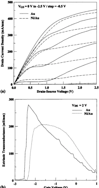
Figure 2(a) shows typical current–voltage characteristics of the studied device with Au and Ni/ Au gate-alloys at 300 K. The device with Au gate shows significant kink ef-fect. The drain current increases rapidly above the threshold voltage 共VGS艌−2 V兲 and at high drain voltage
共VDS⬎1.5 V兲 due to impact ionization and kink effect.
How-ever, the drain current remains low and almost constant at the threshold voltage共VGS= −2.5 V兲. The dependence of the ex-trinsic transconductance共gm兲 on the gate voltage of the stud-ied MHEMT with Au and Ni/ Au gate metals is shown in Fig. 2(b). Sharper transconductance profile near the threshold voltage and poorer gate voltage swing, due to the kink effect, have been observed for the Au gate as compared to that of Ni/ Au gate-alloy. This is attributed to the fact that Ni/ Au has larger barrier height than Au. Though the larger barrier height may reduce the discontinuity of valence band, making the holes easier to be injected into the gate, the depletion region under gate will be significantly extended, conse-quently decreasing the carrier population in the channel. Fig-ure 3 shows the calculated band diagram and the respective electron concentration at thermal equilibrium by the self-consistent method. We have observed that the increase of barrier height 共⌬⌽B兲 is larger than the decrease of valence band discontinuity共⌬EV兲. Due to the dominant influence of the barrier height, the electron concentration is decreased and the kink effect is improved. The typical “bell-shaped” behav-ior observed at different drain-source voltages with Au and Ni/ Au gate, shown in Fig. 4, is related to the occurrence of impact ionization in the channel.12 Due to the present high
electric field in the gate-to-drain region at high VDS,
signifi-cant hot-electron phenomena take place in the channel re-gime. In particular, electrons can obtain enough energy to further generate electron–hole pairs through effective impact ionizations.13The peak gate current density with Ni/ Au gate, in Fig. 4(b), is significantly improved as compared to that of Au gate, in Fig. 4(a). It is the evidence to reduce the impact ionization using gate metal with high barrier height. There-fore, the hole concentration is decreased to prevent the kink effect.
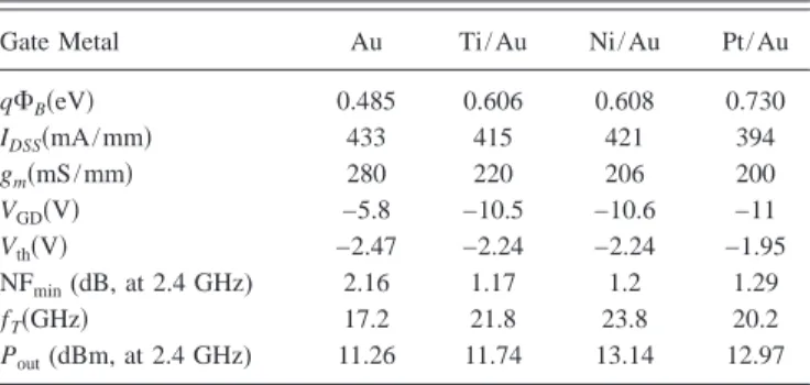
Table I lists the comparisons of dc and rf characteristics for employing various gate alloys. Au-gate has the highest peak extrinsic tranconductance value due to the kink effect. In addition, thanks to the highest barrier height by using Pt/ Au gate alloy, it demonstrates the lowest saturation drain current density, IDSS at VGS= 0 V, the highest gate-to-drain
breakdown voltage, VGD, defined at IGD= 1 mA/ mm, and the FIG. 2.(a) Current–voltage characteristics at 300 K. (b) Extrinsic
transcon-ductance as a function of the gate-source bias at 300 K.
FIG. 3. Schematic band diagram of the studied MHEMT with lower(Au, solid line) and higher (Ni/Au, dash line) barrier height.
5088 Appl. Phys. Lett., Vol. 85, No. 21, 22 November 2004 Chenet al.
threshold voltage, Vth. Because the kink effect can be signifi-cantly suppressed by using Ti/ Au, Ni/ Au, and Pt/ Au alloys, their noise characteristics, the minimum noise figure, NFmin, all excel over that by using Au-gate. Moreover, the Ti/ Au gate alloy demonstrates the best NFmin performance due to its lowest contact resistance. The best output power共Pout兲 is achieved by using the Ni/ Au metal due to the integrated performance of current drive, IDSS, and breakdown
character-istics, VGD. The values of unity current gain cut-off fre-quency共fT兲 for Ti/Au, Ni/Au, and Pt/Au gate-alloys are all above 20 GHz and demonstrate better high-frequency char-acteristics than that of Au-gate.
In summary, comparisons between the MHEMT charac-teristics with various gate-alloys have been made. The domi-nant influences of Schottky height on improving the kink effect and the resulting device performance have also been investigated. Both the kink effect and impact ionization ef-fect can be significantly improved by using the high barrier height gate-alloys, including Ti/ Au, Ni/ Au, and Pt/ Au, re-sulting in the comprehensively superior device gain, thresh-old, noise, power drive, breakdown and high-frequency char-acteristics.
This work was sponsored by the National Science Coun-cil, Republic of China under Contract No. NSC 92-2215-E-006-014.
1
C. Nguyen and M. Micovic, IEEE Trans. Electron Devices 48, 472 (2001).
2
L. D. Nguyen, A. S. Brown, M. A. Thompson, and L. M. Jelloian, IEEE Trans. Electron Devices 39, 2007(1992).
3
H. S. Yoon, J. H. Lee, J. Y. Shim, S. J. Kim, D. M. Kang, J. Y. Hong, W. J. Chang, and K. H. Lee, in 14th Proceedings of Indium Phosphide and Related Materials, 2002, p. 201.
4
K. Ouchi, T. Mishima, M. Kudo, and H. Ohta, Jpn. J. Appl. Phys., Part 1
41, 1004(2002).
5
S. Bollaert, Y. Cordier, M. Zaknoune, H. Happy, S. Lepilliet, A. Cappy, in 13th Proceedings of Indium Phosphide and Related Materials, 2001, p. 192.
6
K. Yuan, K. Radhakrishnan, H. Q. Zheng, and S. F. Yoon, Mater. Sci. Semicond. Process. 4, 641(2001).
7
A. S. Brown, U. K. Mishra, C. S. Chou, C. E. Hooper, M. A. Melendes, M. Thompson, L. E. Larson, S. E. Rosenbaum, and M. J. Delaney, IEEE Electron Device Lett. 10, 565(1989).
8
Y. Hori and M. Kuzubara, IEEE Trans. Electron Devices 41, 2262(1994).
9
T. Suemitsu, H. Fushimi, S. Kodama, S. Tsunashima, and S. Kimura, in 13th Proceedings of Indium Phosphide and Related Materials, 2001, p. 456.
10
T. Suemitsu, T. Enoki, N. Sano, M. Tomizawa, and Y. Ishii, IEEE Trans. Electron Devices 45, 2390(1998).
11
W. E. Hoke, P. S. Lyman, C. S. Whelan, J. J. Mosca, A. Torabi, K. L. Chang, and K. C. Hsieh, J. Vac. Sci. Technol. B 18, 1638(2000).
12
G. Meneghesso, A. Neviani, R. Oesterholt, M. Matloubian, T. Liu, J. J. Brown, C. Canali, and E. Zanoni, IEEE Trans. Electron Devices 46, 2 (1999).
13
M. Boudrissa, E. Delos, C. Gaquiere, M. Rousseau, Y. Cordier, D. Théron, and J. C. De Jaeger, IEEE Trans. Electron Devices 48, 1037(2001). FIG. 4. Gate current density as a function of the gate-source voltage for
various VDS biases with (a) Au gate-metal and (b) Ni/Au gate-metal at 300 K.
TABLE I. Comparisons of dc and rf characteristics by using different gate alloys.
Gate Metal Au Ti/ Au Ni/ Au Pt/ Au
q⌽B共eV兲 0.485 0.606 0.608 0.730 IDSS共mA/mm兲 433 415 421 394 gm共mS/mm兲 280 220 206 200 VGD共V兲 −5.8 −10.5 −10.6 −11 Vth共V兲 −2.47 −2.24 −2.24 −1.95 NFmin(dB, at 2.4 GHz) 2.16 1.17 1.2 1.29 fT共GHz兲 17.2 21.8 23.8 20.2 Pout(dBm, at 2.4 GHz) 11.26 11.74 13.14 12.97
Appl. Phys. Lett., Vol. 85, No. 21, 22 November 2004 Chenet al. 5089