具鎢奈米點埋入之介電層在非揮發性記憶體 元件其製作及研究
160
0
0
全文
(2) 具鎢奈米點埋入之介電層在非揮發性記憶體 元件其製作及研究. 研究生:翁麗雯. 指導教授:張鼎張 博士. 國立中山大學 光電工程研究所碩士班. 摘要 傳統的非揮發性記憶體是利用複晶矽浮停閘(floating gate)作為載子儲存 的單元,而在元件尺寸持續微縮下,此結構將面臨一些瓶頸。為了克服尺寸極限, 近年來衍生出之奈米晶體非揮發性記憶體,即利用半導體或金屬奈米點作為電荷 儲存的單元,可以減少穿隧氧化層的厚度,而不損失可靠性,進而降低操作電壓 及操作速度增快。 在此論文中,將從鎢(W)金屬奈米點的製作方式出發,首先在穿隧氧化層上 方沉積矽化鎢(W5Si3)薄膜,當試片經過高溫熱氧化後,金屬鎢成分會向下在靠近 穿隧氧化層附近成核析出形成鎢奈米點,同時,成份矽則氧化成二氧化矽而將鎢 奈米點包圍,使成為各自獨立的儲存單元。此外,在矽化鎢薄膜製備的過程中, 通入載氣(O2 或 N2),研究鎢金屬奈米點在不同的介電層環境中的記憶效應以及可 靠度分析。同時,本論文也討論額外的氧化矽薄膜沉積在矽化鎢表面對鎢金屬奈 米點的形成機制,可以改善熱氧化的控制能力。厚的氧化矽薄膜可以有效地控制 熱氧化條件,並且防止熱氧化造成的薄膜劣化。然而,過度的熱氧化會造成記憶 窗口下降以及電性劣化,主要是因為部份的鎢金屬奈米點被氧化成含有金屬的介 I.
(3) 電材料。相比之下,我們亦將直接以同時濺鍍鎢及介電材料如二氧化矽(SiO2)或 氮化矽(Si3N4)沉積載子儲存層的方式來形成鎢奈米點包圍在介電層中的結構做 論述。再者,為調變鎢及矽兩者成份含量比例而直接由同時濺鍍沉積的製作也將 於此論文中加以研究。此外,我們也針對鍺成份加入矽化鎢薄膜,對後續鎢金屬 奈米點的記憶窗口以及電性做討論。 總之,由以上的鎢金屬奈米點的製作過程,我們可以得到不同的介電層對傳 統的鎢金屬奈米點記憶體的影響、額外的氧化層對熱處理的影響、以及鍺成份對 記憶效應的貢獻。. II.
(4) Investigation and Fabrication of Nonvolatile Memory Devices with Tungsten Nanocrystals Embedded in Dielectric Layers. Student: Li-Wen Weng. Advisor: Dr. Ting-Chang Chang. Institute of Electrical Optical Engineering National Sun Yat-sen University. Abstract In a conventional nonvolatile memory (NVM), charge is stored in a ploy-silicon floating gate (FG) surrounded by dielectrics. But, it will suffer some limitations for continued scaling of the device structure. Therefore, the nanocrystal nonvolatile memory devices have been investigated to overcome the limit of the conventional floating gate NVM in recently years. Nanocrystal charge storage offers several advantages, the main one being the potential to use thinner tunnel oxide without sacrificing nonvolatility. This is a quite attractive proposition since reducing the tunnel oxide thickness is a key to lowering operating voltage and/or increasing operating speeds. In this thesis, we have fabricated tungsten (W) nanocrystals nonvolatile memory devices. A thin tungsten silicide (W5Si3) layer was deposited on tunnel oxide layer first. The following oxidation was performed in furnace system. The W element tends to segregate downward and precipitate on the tunnel oxide after thermal oxidation. In addition, the silicon element is oxidized into silicon dioxide surrounded tungsten nanocrystals. Also, the carrier gas, such as O2 and N2, were also added as the III.
(5) tungsten silicide deposition. The memory effect and the electrical reliability for W nanocrystals surrounded in different dielectric were also investigated in this study. In addition, the formation mechanism of W nanocrystals with additional silicon oxide capped on tungsten silicide was also investigated. The thicker silicon oxide can effectively control the thermal oxidation condition and prevent thin film degradation. However, the overall oxidation cause the memory window reduction and the electrical characteristics degradation, resulted from the partially oxidation of W nanocrystal to metal-incorporated dielectric. By contrast, we also demonstrated the structure that deposited the charge trapping layer by co-sputtered W and dielectric material as SiO2 or Si3N4 to directly form the W nanocrystal embedded in dielectrics. Besides, the W and Si directly deposited by co-sputtered to adjust the two elements contained ratio had investigated as well in this study. Furthermore, the memory effect and electrical characteristics for germanium (Ge) element incorporated W nanocrystal memory were also discussed. The additional storage element contributes the memory effect. In summary, the memory effect for W nanaocrystal embedded in different dielectric, the effect of the thermal treatment for additional silicon oxide incorporation, and the contribution of the Ge element to the memory effect can be obtained from the fabrication of W nanocrystal memory were finished in this study.. IV.
(6) 誌. 謝. 當著手於致謝的此時,畢業論文也將近完成的階段,研究所的生涯在這裡也 將告結束。一路走來,要感謝的人很多,首先感謝我的指導教授. 張鼎張老師,. 研究所這兩年,在老師身上學到的不僅是專業的學問知識,在研究上獨到的見解 及教學的熱忱,為了實驗室學生花費的精神心力更是令人敬佩;也感謝老師在研 究指導之餘,總是不厭其煩的提醒教導我們待人處事及日後工作上應有的態度。 此外,更感謝老師給我難能可貴的機會,讓我能夠在碩二這一年到新竹學習半導 體製程技術而完成我的畢業論文,有這一年充實的學習機會,讓我在畢業這一 刻,心中充滿踏實的感動。 感謝口試委員鄭子銘博士、王英郎博士及劉柏村老師在論文上的指教及建 議,讓我的論文能夠更加完善,由衷感謝你們。 碩二這一年在新竹的日子,要感謝的人真的太多。感謝劉柏村老師在實驗研 究上給予的指導及建議,更感謝峻豪學長、世青學長、緯仁學長、立偉學長、昭 正學長、志瑋學長等許多學長們總是不厭其煩的提供意見及指教,你們的建議總 是讓我能在實驗遇到瓶頸時找到解決的出口。特別感謝峻豪學長在實驗及論文上 的指導及幫忙,不厭其煩的解決我許多實驗的疑問及提供我更好的建議,今天才 能完成這一份充實的論文,著實受益良多。也感謝這一年一同出入無塵室同甘共 苦的奈米組同學們:俐婷、仕承、睿龍、彥廷、志晟、勝凱,從零開始學習機台 至今一整年的日子,受到你們太多太多的幫助,對你們總是充滿了無限的感激。 還要感謝秀娟、宛芳、亞諭等實驗室的朋友們,經常給我鼓勵及歡笑,有你們真 的很好。此外,與學弟們一同做實驗的時間雖然不多,也感謝有你們讓實驗的日 子裡有更多的歡樂。 感謝中山實驗室的學長同學學弟們,研究所的日子能夠在這個像大家庭的環 境裡生活,受到大家許多的照顧,真心的充滿感激。感謝學長們書瑋、崎峰、原 V.
(7) 瑞、伯鈞等在實驗上的指導及許多的幫助,實驗室的同學靖怡、彩倫、敏甄、怡 萍、峻廷等的朋友們研究上的幫忙與生活上的照顧,及學弟們總是帶給實驗室更 多的歡樂時光,讓我的研究所生活增加許多的溫暖,這一切都將銘記在心。 最後,感謝我最親愛的父母及家人,你們的支持與鼓勵是我在研究的路上前 進的動力,因為有你們的愛讓我在挫折時還能勇敢前行,在疲累時給我依靠的溫 暖及繼續堅持在研究的路上走下去的能量,有你們的支持才能讓我無後顧之憂的 完成碩士班學業;最後的最後,謹以此論文獻給你們。. VI.
(8) Contents. Chinese Abstract --------------------------------------------------------------------------- I English Abstract -------------------------------------------------------------------------- III Acknowledgement ------------------------------------------------------------------------ V Contents ------------------------------------------------------------------------------------ VII Table Captions ----------------------------------------------------------------------------- X Figure Captions --------------------------------------------------------------------------- XI Chapter 1 Introduction 1.1. General Background --------------------------------------------------- 1 1.1.1 SONOS Nonvolatile Memory Devices------------------------- 2 1.1.2 Nanocrystal Nonvolatile Memory Devices--------------------- 4. 1.2. Motivation -------------------------------------------------------------- 6. 1.3. Organization of This Thesis ------------------------------------------ 8. Chapter 2 Basic Principle of Nonvolatile Memory 2.1. Introduction ----------------------------------------------------------- 14. 2.2. Basic Program/Erase Mechanisms --------------------------------- 16 2.2.1 Tunneling Injection ---------------------------------------------- 16 2.2.2 Hot-Election Injection ------------------------------------------- 18 2.2.3 Band to Band Assisted Hole Injection ------------------------ 19. 2.3. Basic Reliability of Nonvolatile Memory ------------------------- 19 2.3.1 Retention ---------------------------------------------------------- 20. VII.
(9) 2.3.2 Endurance --------------------------------------------------------- 20 2.4. Basic Physical Characteristic of Nanocrystals NVMs ---------- 20 2.4.1 Quantum Confinement Effect ---------------------------------- 20 2.4.2 Coulomb Blockade Effect -------------------------------------- 21. Chapter 3 Formation of W-NCs Nonvolatile Memory 3.1. Motivation ------------------------------------------------------------- 28. 3.2. Experimental Procedures -------------------------------------------- 30. 3.3. Results and Discussion ---------------------------------------------- 31. 3.4. Conclusions ----------------------------------------------------------- 35. Chapter 4 Applications of Oxygen/Nitrogen-Incorporated W-NCs NVMs 4.1. Motivation ------------------------------------------------------------- 43. 4.2. Experimental Procedures -------------------------------------------- 43. 4.3. Results and Discussion ---------------------------------------------- 45. 4.4. Conclusions ----------------------------------------------------------- 49. Chapter 5 Comparison of W-NCs Embedded in Dielectric Layers 5.1. ESCA Analyses of W-NCs Embedded in Dielectric Layers --------------------------------------------------------------------------- 63. 5.2. Effect of Capped Oxide for W-NCs Formation in Dielectric Layers ------------------------------------------------------------------ 67 5.2.1 Capacitance-Voltage Characteristics--------------------------- 67 5.2.2 Secondary Ion Mass Spectroscopy (SIMS) Analyses for Oxidized W-Si (O/N) Layers w/o Capped 20-nm-thick Oxide ---------------------------------------------------------------------- 69. VIII.
(10) 5.3. Discussions of Non-ideal C-V Hysteresis of W-NCs Nonvolatile Memory ---------------------------------------------------------------- 72. 5.4. Conclusions ----------------------------------------------------------- 73. Chapter 6 W-doped SiO2/Si3N4 as Self-assembling Layers of W-NCs 6.1. Motivation ------------------------------------------------------------- 93. 6.2. Experimental Procedures -------------------------------------------- 93. 6.3. Results and Discussion ---------------------------------------------- 94. 6.4. Conclusions ----------------------------------------------------------- 97. Chapter 7 W-incorporated Si/Si1-xGex (x=0.5) as Self-assembling Layers of W-NCs 7.1. Motivation ----------------------------------------------------------- 108. 7.2. Experimental Procedures ------------------------------------------ 108. 7.3. Results and Discussion --------------------------------------------- 110. 7.4. Conclusions ---------------------------------------------------------- 115. Chapter 8 Conclusions 8.1. Conclusions ---------------------------------------------------------- 129. Chapter 9 Future Work ------------------------------------------------------------ 132 References --------------------------------------------------------------------------------- 134 Vitae ------------------------------------------------------------------------------------------ 142. IX.
(11) Table Captions. Chapter 5 Table 5-1 The comparison with the W-O bonds oxidized ratios of O 1s ESCA spectra and corresponding memory windows under ±5V operation in structure I, structure II and structure III with oxidation 30 minutes.. Chapter 6 Table 6-1 The comparison of memory windows in structure IV and structure V under ±7V operation with their corresponding oxidative conditions.. Chapter 7 Table 7-1 The comparison of memory windows in structure VII with capped 20nm and capped 10nm oxide before oxidation under ±5V operation with their corresponding oxidative conditions.. X.
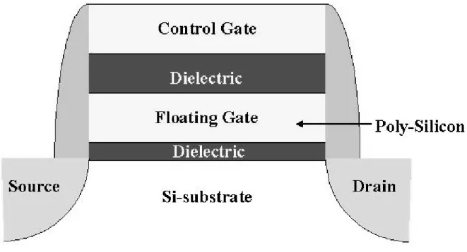
(12) Figure Captions. Chapter 1 Figure 1-1 The structure of the conventional floating gate nonvolatile memory device. Continuous poly-Si floating gate is used as the charge storage element. Figure 1-2 The structure of the SONOS nonvolatile memory device. The nitride layer is used as the charge-trapping element. Figure 1-3 The development of the gate stack of SONOS EEPROM memory devices. The optimization of nitride and oxide films has been the main focus in recent years. Figure 1-4 The energy band diagrams of the write/erase operation for a SONOS device. Figure 1-5 The structure of the nanocrystal nonvolatile memory device. The semiconductor nanocrystals or metal nano-dots are used as the charge storage element instead of the continuous poly-Si floating gate.. Chapter 2 Figure 2-1 I–V curves of an FG device when there is no charge stored in the FG (curve A) and when a negative charge Q is stored in the FG (curve B). Figure 2-2 Energy band diagrams of a dual-channel SONOS transistor under (a) positive and (b) negative gate bias. (●: electrons; ○: holes) Figure 2-3 (a) Schematic cross-section of nanocrystal memory device structure; (b) illustration of write process: inversion- layer electron tunnels into the nanocrystal; (c) illustration of erase process: accumulation layer hole XI.
(13) tunnels into the nanocrystal, electron in nanocrystal can tunnel back to the channel. Figure 2-4 SONOS ideal energy band diagram. Figure 2-5 Fourth approaches to programming methods, described by Hu and White. Figure 2-6 Schematic cross section of MOSFET. The energy-distribution function at point (X1, Y1) is also shown.. Chapter 3 Figure 3-1 The process flow of structure I in this work. Figure 3-2 The C-V hystereses of structure I with (a) oxidation 30 minutes (b) oxidation 45 minutes and (c) oxidation 60 minutes. Figure 3-3 The I-V characteristics of structure I with oxidation 30 minutes, oxidation 45 minutes and oxidation 60 minutes, respectively. Figure 3-4 Transmission electron microscopy (TEM) analysis of structure I (a) without oxidation, (b) with oxidation 30 minutes, (c) with oxidation 45 minutes and (d) with oxidation 60 minutes, respectively. The insert is the TEM analysis by adjusting contrast. Figure 3-5 The mechanism of structure I during thermal oxidation in furnace. Figure 3-6 The endurance characteristics after different write/erase cycles of structure I with (a) oxidation 30 minutes (b) oxidation 45 minutes and (c) oxidation 60 minutes. Figure 3-7 The charge retention characteristic of structure I with 60 minutes thermal oxidation.. XII.
(14) Chapter 4 Figure 4-1 The process flow of (a) structure II and (b) structure III in this work. Figure 4-2 The C-V hystereses of structure II with (a) oxidation 30 minutes (b) oxidation 45 minutes and (c) oxidation 60 minutes. Figure 4-3 The I-V characteristics of structure II with oxidation 30 minutes, oxidation 45 minutes and oxidation 60 minutes, respectively. Figure 4-4 Transmission electron microscopy (TEM) analysis of structure II (a) without oxidation, (b) with oxidation 30 minutes, (c) with oxidation 45 minutes and (d) with oxidation 60 minutes, respectively. The insert is the TEM analysis by adjusting contrast. Figure 4-5 The mechanism of structure II during thermal oxidation in furnace. Figure 4-6 Endurance characteristics after different write/erase cycles of structure II with (a) oxidation 30 minutes (b) oxidation 45 minutes and (c) oxidation 60 minutes. Figure 4-7 The charge retention characteristic of structure II with 60 minutes thermal oxidation. Figure 4-8 The C-V hystereses of structure III with (a) oxidation 30 minutes (b) oxidation 45 minutes and (c) oxidation 60 minutes. Figure 4-9 The I-V characteristics of structure III with oxidation 30 minutes, oxidation 45 minutes and oxidation 60 minutes, respectively. Figure 4-10 Transmission electron microscopy (TEM) analysis of structure III (a) without oxidation, (b) with oxidation 30 minutes, (c) with oxidation 45 minutes and (d) with oxidation 60 minutes, respectively. The insert is the TEM analysis by adjusting contrast. Figure 4-11 The mechanism of structure III during thermal oxidation in furnace. Figure 4-12 Endurance characteristics after different write/erase cycles of structure XIII.
(15) III with (a) oxidation 30 minutes (b) oxidation 45 minutes and (c) oxidation 60 minutes. Figure 4-13 The charge retention characteristic of structure III with 60 minutes thermal oxidation.. Chapter 5 Figure 5-1 The ESCA spectra of W 4f peaks in structure I without oxidation. Figure 5-2 The ESCA spectra of W 4f peaks in structure II without oxidation. Figure 5-3 The ESCA spectra of W 4f peaks in structure III without oxidation. Figure 5-4 The ESCA spectra of N 1s peaks in structure III without oxidation. Figure 5-5 The ESCA spectra of O 1s peaks in structure I: as-deposited and after oxidation for 30 minutes. The insert shows the percentage of each peak’s area in the STD structure occupied in the whole spectra area. Figure 5-6 The ESCA spectra of O 1s peaks in structure I after 30 minutes oxidation. The insert shows the percentage of each peak’s area occupied in the whole spectra area. Figure 5-7 The ESCA spectra of O 1s peaks in structure II: as-deposited and after oxidation for 30 minutes. The insert shows the percentage of each peak’s area in the STD structure occupied in the whole spectra area. Figure 5-8 The ESCA spectra of O 1s peaks in structure II after 30 minutes oxidation. The insert shows the percentage of each peak’s area occupied in the whole spectra area. Figure 5-9 The ESCA spectra of O 1s peaks in structure III: as-deposited and after oxidation for 30 minutes. The insert shows the percentage of each peak’s area in the STD structure occupied in the whole spectra area. Figure 5-10 The ESCA spectra of O 1s peaks in structure III after 30 minutes XIV.
(16) oxidation. The insert shows the percentage of each peak’s area occupied in the whole spectra area. Figure 5-11 The C-V hysteresis of structure I (a) without capped oxide (b) with capped 5nm oxide (c) with capped 10nm oxide and (d) with capped 20nm oxide before oxidation, respectively. The insert of each diagram was their corresponding structure. Figure 5-12 The C-V hysteresis of structure II (a) without capped oxide (b) with capped 5nm oxide (c) with capped 10nm oxide and (d) with capped 20nm oxide before oxidation, respectively. The insert of each diagram was their corresponding structure. Figure 5-13 The C-V hysteresis of structure III (a) without capped oxide (b) with capped 5nm oxide (c) with capped 10nm oxide and (d) with capped 20nm oxide before oxidation, respectively. The insert of each diagram was their corresponding structure. Figure 5-14 The SIMS analysis of structure I: (a) without capped oxide and (b) with capped 20nm oxide, and their corresponding C-V hysteresis showed in (c) and (d), respectively. Figure 5-15 The SIMS analysis of structure II: (a) without capped oxide and (b) with capped 20nm oxide, and their corresponding C-V hysteresis showed in (c) and (d), respectively. Figure 5-16 The SIMS analysis of structure III: (a) without capped oxide and (b) with capped 20nm oxide, and their corresponding C-V hysteresis showed in (c) and (d), respectively. Figure 5-17 The oxidation mechanism in structure I (a) without capped oxide and (b) with capped 20nm oxide before oxidation.. XV.
(17) Chapter 6 Figure 6-1 The process flow of (a) structure IV and (b) structure V in this work. Figure 6-2 The C-V hystereses of structure IV with (a) oxidation 30 minutes (b) oxidation 45 minutes and (c) oxidation 60 minutes. Figure 6-3 The C-V hystereses of structure V with (a) oxidation 30 minutes (b) oxidation 45 minutes and (c) oxidation 60 minutes. Figure 6-4 The band diagrams for charge trapping centers as (a) W nanocrystal embedded in SiO2 layer and (b) W nanocrystal embedded in SiON layer, respectively. Figure 6-5 The I-V characteristics of structure IV with oxidation 30 minutes, oxidation 45 minutes and oxidation 60 minutes, respectively. Figure 6-6 The I-V characteristics of structure V with oxidation 30 minutes, oxidation 45 minutes and oxidation 60 minutes, respectively. Figure 6-7 Endurance characteristics after different write/erase cycles of structure IV with (a) oxidation 30 minutes (b) oxidation 45 minutes and (c) oxidation 60 minutes. Figure 6-8 Endurance characteristics after different write/erase cycles of structure V with (a) oxidation 30 minutes (b) oxidation 45 minutes and (c) oxidation 60 minutes.. Chapter 7 Figure 7-1 The process flow of structure VI in this work. Figure 7-2 The process flow of structure VII (a) with capped 20nm oxide and (b) with capped 10nm oxide before oxidation in this work. Figure 7-3 The C-V hystereses of capped 20nm oxide in structure VI with (a) oxidation 30 minutes (b) oxidation 45 minutes and (c) oxidation 60 XVI.
(18) minutes. Figure 7-4 The band diagrams of structure VI during thermal oxidation. Figure 7-5 The I-V characteristics of structure VI with oxidation 30 minutes, oxidation 45 minutes and oxidation 60 minutes, respectively. Figure 7-6 The C-V hystereses of capped 20nm oxide before oxidation in structure VII with oxidation (a) 30 minutes (b) 45 minutes and (c) 60 minutes. Figure 7-7 The I-V characteristics of capped 20nm oxide before oxidation in structure VII with oxidation 30 minutes, oxidation 45 minutes and oxidation 60 minutes, respectively. Figure 7-8 The C-V hystereses of capped 10nm oxide before oxidation in structure VII with oxidation (a) 30 minutes (b) 45 minutes and (c) 60 minutes. Figure 7-9 The I-V characteristics of capped 10nm oxide before oxidation in structure VII with oxidation 30 minutes, oxidation 45 minutes and oxidation 60 minutes, respectively. Figure 7-10 Transmission electron microscopy (TEM) analyses of (a) capped 20nm oxide and (b) capped 10nm oxide before oxidation in structure VII with oxidation for 45 minutes, respectively. The insert is the TEM analysis by adjusting contrast. Figure 7-11 The Raman spectra of capped 20nm oxide before oxidation in structure VII with oxidation 30 minutes, oxidation 45 minutes and oxidation 60 minutes, respectively. Figure 7-12 The Raman spectra of capped 10nm oxide before oxidation in structure VII with oxidation 30 minutes, oxidation 45 minutes and oxidation 60 minutes, respectively.. XVII.
(19) Chapter 1. Introduction. 1.1 General Background In recent years, the portable electronic product have widely applied, such as digital cameras, MP3 players, personal digital assistants (PDA), mobile phones, and external data storage devices for personal computers, USB Flash personal disc ,etc., and play an important role in the market. These products all are based on flash memory. Since the flash memories have evolved from single device components to megabit non-volatile memory (NVM) arrays [1.1]. Flash memories are easily scalable replacements for EPROMs (Erasable Programmable Read Only Memory) and EEPROMs (Electrically Erasable Programmable Read Only Memory). Unlike EPROMs and EEPROMs, flash memory cells provide single-cell electrical program and fast simultaneous block electrical erase. The operation principal of conventional Flash memory is using the polycrystalline silicon as floating gate to be the charge stored units. After electrons which injected from the channel stored in floating gate, the threshold voltage of devices will be changed. The logical “0” and “1” definition of nonvolatile memory devices are used for the difference between threshold voltages. In 1967, D. Kahng and S. M. Sze invented the floating-gate (FG) nonvolatile semiconductor memory (or flash memory) at Bell Labs [1.2]. The stacked-gate FG device structure is shown in Figure1-1. Although a huge commercial success, conventional FG devices have their limitations. The most prominent one is the limited potential for continued scaling of the device structure. This scaling limitation stems from the extreme requirements put on the tunnel oxide layer. The tunnel oxide must 1.
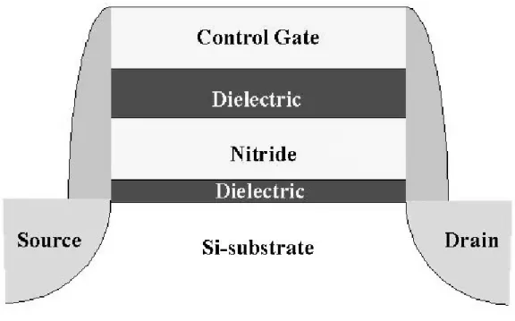
(20) be thin enough to allow quick and efficient charge transfer to and from the FG. On the other hand, the tunnel oxide needs to provide superior isolation under retention, endurance, and disturbed conditions in order to maintain information integrity over periods of up to a decade. When the tunnel oxide is thinner for operation speed consideration, the retention characteristics may be degraded. And when the tunnel oxide is made thicker to take the isolation into account, the speed of the operation will be slower. Therefore, there is a tradeoff between speed and reliability and the thickness of the tunnel oxide is compromised to about 8-11 nm, which is barely reduced over more than five successive generations of the industry [1.3]. The other prominent limitation in conventional FG memory devices is the quality and strength of tunnel oxide (or tunnel dielectric) after plenty of program/erase cycles. Once a leaky path has been created in tunnel oxide, all the charges stored in the floating gate will be lost. Therefore, two suggestions, poly-Si/oxide/nitride/oxide/Si (SONOS) [1.4-1.6] and nanocrystal nonvolatile memory devices [1.7-1.9], are proposed to overcome this oxide quality limit of the conventional FG structure. These technologies replace the floating gate structure with a great number of charge-storage nodes in the dielectric or in the nanocrystal. Unlike the floating gate, stored charges in isolated nodes cannot easily redistribute amongst themselves and the local leaky path will not cause the fatal loss of information for the nanocrystal nonvolatile memory device. This effectively prevents the leakage of all the stored charges out of the floating gate.. 1.1.1 SONOS Nonvolatile Memory Devices Poly-Si/SiO2/Si3N4/SiO2/Si (SONOS) nonvolatile memory devices structure shown in Fig. 1-2, the charge storage elements in SONOS memory are the charge. 2.
(21) traps distributed throughout the volume of the Si3N4 layer. A typical trap has a density of the order 1018-1019 cm-3 according to Yang et al [1.10] and stores both electrons and holes (positive charges) injected from the channel. Figure 1-3 illustrates the progression of device cross section, which has led to the present SONOS device structure. The nitride-base memory devices were extensively studied. in. the. early. 70s. after. the. first. metal-gate. nitride. device. Metal/Nitride/Oxide/Silicon (MNOS) was reported in 1967 by Wegener et al [1.11]. Initial device structures in the early 1970s were p-channel metal-nitride-oxide-silicon (MNOS) structures with aluminum gate electrodes and thick (45 nm) silicon nitride charge storage layers. Write/erase voltages were typically 25-30 V. In the late 1970s and early 1980s, scaling moved to n-channel silicon-nitride-oxide-silicon (SNOS) devices with write/erase voltages of 14-18 V. In the late 1980s and early 1990s, n- and p-channel SONOS devices emerged with write/erase voltages of 5-12 V. In the SONOS device, an oxide layer is introduced between the gate and the nitride region. Thus, it forms the SiO2/Si3N4/SiO2 (ONO) gate dielectric stack, as previous shown in Fig. 1-2, instead of capping the nitride layer with just a metal or semiconductor gate. The purpose of the top blocking oxide is to reduce the charge injection from the control gate into the nitride layer, limiting the memory window of both MNOS and SNOS devices. The program/erase mechanism is shown in Fig. 1-4. During programming, the control gate is biased positively so that electrons from the channel can tunnel across the SiO2 into the nitride layer. Some electrons will continue to move through the nitride layer then across the control oxide finally into the control gate. The remaining trapped charges in the nitride layer provide the electrostatic screening of the channel from the control gate. Therefore, there is a threshold voltage shift (ΔVT) resulting from trapped charges in nitride and because of that SONOS can be used as a memory 3.
(22) device just like conventional floating gate devices.. 1.1.2 Nanocrystal Nonvolatile Memory Devices Nanocrystal nonvolatile memories first introduced in the early 1990s. IBM researchers first proposed flash memory with a granular floating gate made out of silicon nanocrystals [1.12]. Figure1-5 illustrates Nanocrystal nonvolatile memory device structures. In a nanocrystal NVM device, charge is not stored on a continuous FG poly-Si layer, but instead on a layer of discrete, mutually isolated, crystalline nanocrystals or dots. Each dot will typically store only a handful of electrons; collectively the charges stored in these dots control the channel conductivity of the memory transistor. The charges loss through lateral paths in nanocrystal-based memory devices can be suppressed by the oxide isolation between nanocrystals, these devices exhibited superior charge storage characteristics compared with conventional floating-gate memory devices. All stored charges can’t be lost through the few leaky paths since the charges are stored in distributed nano-dots. As compared to conventional stacked gate NVSM devices, nanocrystal charge storage offers several advantages, the main one being the potential to use thinner tunnel oxide without sacrificing nonvolatility. This is a quite attractive proposition since reducing the tunnel oxide thickness is a key to lowering operating voltages and/or increasing operating speeds. This claim of improved scalability results not only from the distributed nature of the charge storage, which makes the storage more robust and fault-tolerant, but also from the beneficial effects of Coulomb blockade [1.13]. Quantum confinement effects (bandgap widening; energy quantization) can be exploited in sufficiently small nanocrystal geometries (sub-3 nm dot diameter) to further enhance the memory’s performance.. 4.
(23) Due to the less drain to FG coupling, nanocrystal memories suffer less from drain induced barrier lowering (DIBL). One way to exploit this advantage is to use a higher drain bias during the read operation, thus improving memory access time [1.14]. There is other particular importance as the low capacitive coupling between the external control gate and the nanocrystal charge storage layer. This does not only results in higher operating voltages, thus offsetting the benefits of the thinner tunnel oxide, but also removes an important design parameter (the coupling ratio) typically used to optimize the performance and reliability tradeoff. Unlike volume distributed charge traps (ex: nitride in SONOS NVM), nanocrystals be deposited in a two-dimensional layer at a fixed distance from the channel separated by a thin tunnel oxide. By limiting nanocrystals deposition to just one layer and adjusting the thickness of the top blocking dielectric, charge leakages to the control gate from the storage nodes can be effectively prevented. Moreover, in optimizing NVM devices, the approach which is the focus of this study is to engineer the depth of the potential well at the storage nodes. It is said that creating an asymmetrical barrier between the substrate and the storage nodes, i.e., a small barrier for writing and a large barrier for retention. This can be achieved if the storage nodes are made of metal nanocrystals. The major advantages of metal nanocrystals over their semiconductor counterparts include higher density of states around the Fermi level, stronger coupling with the conduction channel, a wide range of available work functions, and smaller energy perturbation due to carrier confinement. Nanocrystal memories have been presented in the mid-nineties as a possible alternative to conventional FG NVMs devices, by allowing a further decrease in the tunnel oxide thickness. Research in this area has focused on the development of nanocrystal materials and fabrication processes, and on the integration of 5.
(24) nanocrystal-based storage layers in actual memory devices. Promising device results have been presented such as demonstrating low-voltage operation for comparable threshold voltage windows. In spite of these results, it is unclear whether nanocrystal memories will ever see commercialization. In order for that to happen, the uniformity of the nanocrystals needs to be improved, and the claimed benefits need to be more unambiguously substantiated.. 1.2 Motivation The Semiconductor Industry Association (SIA) International Technology Roadmap for Semiconductors (ITRS) indicates the difficult challenge, beyond the year 2005, for nonvolatile semiconductor memories is to achieve reliable, low-power, low-voltage performance [1.15]. For nonvolatile flash memories, two limitations encountered at the present time are: (1) the limited potential for continued scaling of the device structure. This scaling limitation stems from the extreme requirements put on the tunnel oxide layer. In order to get balance between program/erase speed and retention time, there is a trade-off between speed and reliability to get the optimal tunnel oxide thickness. (2) the quality and strength of tunnel oxide (or tunnel dielectric) after plenty of program/erase cycles. Once a leaky path has been created in tunnel oxide, all the charges stored in the floating gate will be lost. Therefore, the nanocrystal nonvolatile memory devices have been investigated to overcome the limits of the conventional floating gate NVM in recently years. Nanocrystal charge storage offers several advantages, the main one being the potential to use thinner tunnel oxide without sacrificing nonvolatility. This is a quite attractive proposition since reducing the tunnel oxide thickness is a key to lowering operating voltage and/or increasing operating speeds.. 6.
(25) In this thesis, we have fabricated tungsten (W) nanocrystals nonvolatile memory device. A thin tungsten silicide (W5Si3) layer was deposited on tunnel oxide layer first. The following oxidation was performed in furnace system. The W element tends to segregate downward and precipitate on the tunnel oxide after thermal oxidation. In addition, the silicon element is oxidized into silicon dioxide surrounded tungsten nanocrystals. Also, the carrier gas, such as O2 and N2, were also added as the tungsten silicide deposition. The memory effect and the electrical reliability for W nanocrystals surrounded in different dielectric were also investigated in this study. In addition, the formation mechanism of W nanocrystals with additional silicon oxide capped on tungsten silicide was also investigated. The thicker silicon oxide can effectively control the thermal oxidation condition and prevent thin film degradation. However, the overall oxidation cause the memory window reduction and the electrical characteristics degradation, resulted from the partially oxidation of W nanocrystal to metal-incorporated dielectric. By contrast, we also demonstrated the structure that deposited the charge trapping layer by co-sputtered W and dielectric material as SiO2 or Si3N4 to directly form the W nanocrystal embedded in dielectrics. Besides, the W and Si directly deposited by co-sputtered to adjust the two elements contained ratio had investigated as well in this study. Furthermore, the memory effect and electrical characteristics for germanium (Ge) element incorporated W nanocrystal memory were also discussed in this study.. 7.
(26) 1.3 Organization of This Thesis In chapter 1, general background of flash nonvolatile memory, SONOS nonvolatile memory and nanocrystal nonvolatile memory devices were introduced. In chapter 2, basics of program/erase operation for memory device were discussed. In chapter 3, the formation of W-NCs nonvolatile memory from the charge storage layer deposited by commixed W5Si3 target was stated. In chapter 4, the applications of oxygen/nitrogen-incorporated W-NCs NVMs were investigated. In chapter 5, the comparisons of W-NCs embedded in dielectric layers by ESCA analyses were discussed. The effect of capped oxide for W-NCs formation was also presented. In chapter 6, the W-doped SiO2/Si3N4 as self-assembling layers of W-NCs was proposed. In chapter 7, the W-incorporated Si/Si1-xGex (x=0.5) as self-assembling layers of W-NCs was also investigated. Finally, the conclusion is presented in chapter 8.. 8.
(27) Figure 1-1 The structure of the conventional floating gate nonvolatile memory device. Continuous poly-Si floating gate is used as the charge storage element.. 9.
(28) Figure 1-2 The structure of the SONOS nonvolatile memory device. The nitride layer is used as the charge-trapping element.. 10.
(29) Figure 1-3 The development of the gate stack of SONOS EEPROM memory devices. The optimization of nitride and oxide films has been the main focus in recent years.. 11.
(30) Figure 1-4 The energy band diagrams of the write/erase operation for a SONOS device.. 12.
(31) Figure 1-5 The structure of the nanocrystal nonvolatile memory device. The semiconductor nanocrystals or metal nano-dots are used as the charge storage element instead of the continuous poly-Si floating gate.. 13.
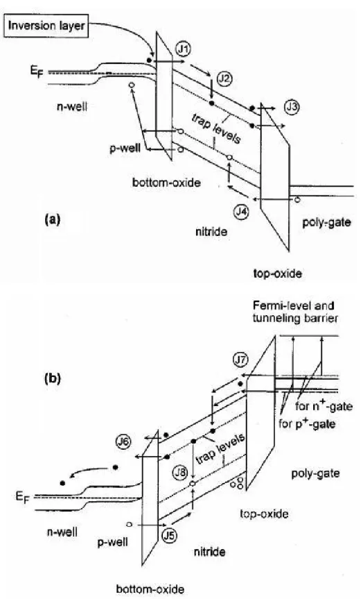
(32) Chapter 2. Basic Principle of Nonvolatile Memory. 2.1 Introduction Most of operations on novel nonvolatile memories, such as nanocrystal and SONOS memories are base on the concept of Flash memory. If a datum has to be stored in a bit of the memory, there are different procedures. The threshold voltage shift of a Flash transistor can be written as [2.1-2.2]: ΔVT = −. Q CFC. where Q is the charge weighted with respect to its position in the gate oxide, and the capacitances between the floating gate and control gate. The threshold voltage of the memory cell can be altered by changing the amount of charge present between the gate and the channel, corresponding to the two states of the memory cell, i.e., the binary values (“1” and “0”) of the stored bit. Fig. 2-1 shows the threshold voltage shift between two states in a Flash memory. To a nonvolatile memory, it can be “written” into either state “1” or “0” by either “programming” or “erasing” methods, which are decided by the definition of memory cell itself. There are many solutions to achieve “programming” or “erasing”. The energy band diagrams for the SONOS structure for positive (write) and negative gate bias (erase), and the main conduction mechanisms, are illustrated in Fig. 14.
(33) 2-2. Under positive gate bias electron injection from the semiconductor to the nitride (J1) will dominate. In the nitride electrons are trapped and drift toward the top oxide by the Poole–Frenkel conduction (J2) [2.3]. The electrons reaching the top oxide may tunnel through it to be collected by the gate (J3). Hole injection from the gate (J4) is negligible for two reasons: First, the top oxide is thicker than the bottom oxide. Second, in oxide the potential barrier for holes (qψB=3.1eV) is higher than for electrons (qψBh=3.8eV). Under negative gate bias either holes are injected from the semiconductor into the nitride (J5) or the electrons previously injected by a write-pulse back-tunnel into the substrate (J6). Electrons are easily injected from the gate (J7) due to the lower potential barrier. The electrons and holes may recombine in the nitride (J8). The write and erase processes for an n-channel semiconductor nanocrystal memory device are illustrated schematically in Fig. 2-3. During the write process, a positive gate voltage is applied to inject channel inversion-layer electrons into the nanocrystals. During the erase process, a reverse gate bias is applied to cause the electrons to tunnel back into the channel and the accumulation layer holes to tunnel into the nanocrystal from the channel [2.4]. The relation between bias and energy band bending is a key to understand basics program and erase mechanisms. Fig. 2-4 shows energy band diagram of SONOS. The barrier of SiO2 is about 3.1eV for electrons in the conduction band of silicon, and 4.78eV for holes in valance band. The barrier of Si3N4 is about 1.05eV for electrons in the conduction band of nitride, and 2.85eV for holes in valance band, the gap for electron between conduction band and trapping level is 0.7eV, and, for hole between valance band and trapping level is 0.95eV [2.5]. In this chapter, we will discuss program/erase mechanisms from the relation 15.
(34) between bias and energy band bending. Fowler-Nordheim tunneling, hot electron injection, band to band assisted hole injection, channel hole injection will be discussed briefly. The reliability of nonvolatile memory and physical characteristic of nanocrystal NVMs will be also discussed.. 2.2 Basic Program/Erase Mechanisms 2.2.1 Tunneling Injection Tunneling is a quantum mechanical process akin to throwing as ball against a wall often enough that the ball goes through the wall without damaging the wall or the ball. It also loses no energy during the tunnel event. The probability of this event happening, however, is extremely low, but an electron incident on a barrier typically several nm thick has a high probability of transmission. Basically, tunneling injection must to have available states on the other side of the barrier for the carriers to tunnel into. Tunneling through the oxide can be attributed to different carrier-injection mechanisms. Which process applies depends on the oxide thickness and the applied gate field or voltage. Direct tunneling (DT), Fowler-Nordheim tunneling (FN), modified Fowler-Nordheim tunneling (MFN) and trap assistant tunneling (TAT) are the main programming mechanisms employed in memory [2.6-2.8], as shown in Figure 2-5. Direct Tunneling Direct Tunneling is the flow of electrons through the full oxide thickness illustrated in Fig. 2-6. For nanocrystal memories, the control-gate coupling ratio of nanocrystal memory devices is inherently small [2.9]. As a result, F-N tunneling cannot serve as an efficient write/erase mechanism when a relatively thick tunnel 16.
(35) oxide is used, because the strong electric field cannot be confined in one oxide layer. The direct tunneling is employed in nanocrystal memories instead. In the direct-tunneling regime, a thin oxide with thickness less than 3 nm is used to separate the nanocrystals from the channel. During write/erase operations, electrons/holes can pass through the oxide by direct tunneling, which gives the advantages of fast write/erase and low operation voltage. In the other hand, the direct tunneling is more sensitive to the barrier width than barrier height, two to four orders of magnitude reduction in leakage current can still be achieved if large work function metals, such as Au or Pt [2.10]. Fowler–Nordheim Tunneling The Fowler–Nordheim (FN) tunneling is the flow of electrons through a triangular potential barrier illustrated in Fig. 2-5. FN tunneling mechanism occurs when applying a strong electric field (in the range of 8–10 MV/cm) across a thin oxide. In these conditions, the energy band diagram of the oxide region is very steep. Therefore, there is a high probability of electrons’ passing through the energy barrier itself. Using a free-electron gas model for the metal and the WKB approximation for the tunneling probability [2.11], one obtains the following expression for current density [2.12]:. ⎡ − 4(2m∗ ) 12 Φ 3 2 ⎤ q3 F 2 OX B ⎥ J= exp ⎢ 16π 2 h 2Φ B 3 η qF ⎥⎦ ⎢⎣ ∗ Where ФB is the barrier height, mOX is the effective mass of the electron in the. forbidden gap of the dielectric, h is the Planck’s constant, q is the electronic charge, and F is the electric field through the oxide. The exponential dependence of tunnel current on the oxide-electric field causes some critical problems of process control. 17.
(36) because, for example, a very small variation of oxide thickness among the cells in a memory array produces a great difference in programming or erasing currents, thus spreading the threshold voltage distribution in both logical states. Modified Fowler–Nordheim Tunneling. Modified Fowler–Nordheim tunneling (MFN) is similar to the traditional FN tunneling mechanism, yet the carriers enter the nitride at a distance further from the tunnel oxide-nitride interface. MFN mechanism is frequently observed in SONOS memories. The SONOS memory is designed for low-voltage operation (<10V, depending on the equivalent oxide thickness), a relatively weak electrical field couldn’t inject charges by DT or FN mechanism. Trap Assistant Tunneling. The charge storage mediums with many traps may cause another tunneling mechanism. For example, the charges tunnel through a thin oxide and arrive to the traps of nitride layer at very low electrical field in SONOS systems. During trap assisted injection the traps are emptied with a smaller time constant then they are filled. The charge carriers are thus injected at the same distance into the nitride as for MFN injection. Because of the sufficient injection current, trap assistant tunneling may influence in retention [2.13].. 2.2.2 Hot-Electron Injection The physical mechanism of HEI is relatively simple to understand qualitatively. An electron traveling from the source to the drain gains energy from the lateral electric field and loses energy to the lattice vibrations (acoustic and optical phonons). At low fields, this is a dynamic equilibrium condition, which holds until the field. 18.
(37) strength reaches approximately 100kV/cm [2.14]. For fields exceeding this value, electrons are no longer in equilibrium with the lattice, and their energy relative to the conduction band edge begins to increase. Electrons are “heated” by the high lateral electric field, and a small fraction of them have enough energy to surmount the barrier between oxide and silicon conduction band edges (channel hot electron, CHE). Figure 2-5 shows schematic representation of CHEI MOSFET and the energy-distribution function with different fields. In the other hand, the effective mass of hole is heavier than one of electron. It is too hard to obtain enough energy to surmount oxide barrier. Therefore, hot-hole injection rarely is employed in nonvolatile memory operation.. 2.2.3 Band to Band Assisted Hole Injection In N-channel, when a negative gate voltage and a positive drain voltage are applied to the cell, electron-hole pairs are generated by BTBT in the drain region [2.15-2.16]. The holes are accelerated by a lateral electric field toward the channel region and some of them obtain high energy. The injection of such hot holes [2.17] into nitride through the tunnel oxide is used for a new erase operation in N-channel.. 2.3 Basic Reliability of Nonvolatile Memory For a nonvolatile memory, the important to concern is distinguishing the state in cell. However, in many times operation and charges storage for a long term, the state is not obvious with charges loss. Endurance and retention experiments are performed to investigate Flash-cell reliability.. 19.
(38) 2.3.1 Retention Retention describes the ability to the NVMs to store and recover information after a number of program cycles at a specified temperature. In any nonvolatile memory technology, it is essential to retain data for over ten years. This means the loss of charge stored in the storage medium must be as minimal as possible. For example, in modern Flash cells, FG capacitance is approximately 1 fF. A loss of only 1 fC can cause a 1V threshold voltage shift. If we consider the constraints on data retention in ten years, this means that a loss of less than five electrons per day can be tolerated [2.18]. Possible causes of charge loss are: 1) by tunneling or thermionic emission mechanisms; 2) defects in the tunnel oxide; and 3) detrapping of charge from insulating layers surrounding the storage medium.. 2.3.2 Endurance Endurance is the number of write/erase operations that the memory will complete and continue to operate as specified in the data sheet. In a conventional Flash memory the maximum number of program/erase cycles that the device must sustain is 106. Many researchers have observed excellent endurance behavior on nanocrystal memories, showing only limited threshold voltage window closure after more than 106 write/erase cycles [2.19-2.21].. 2.4 Basic Physical Characteristic of Nanocrystal NVMs 2.4.1 Quantum Confinement Effect The quantum confinement energy dependence on nanocrystal size has been. 20.
(39) studied both experimentally and theoretically with the tight-binding model [2.20]. The quantum confinement effect becomes significant when the nanocrystal size shrinks to the nanometer range, which causes the conduction band in the nanocrystal to shift to higher energy compared with bulk material [2.23]. The quantum confinement energy dependence on nanocrystal size has been studied both experimentally and theoretically with the tight-binding model [2.24]. Compared with bulk Ge, a 3nm Ge nanocrystal can have a conduction band shift of 0.5eV, which is significant enough to affect the electrical performance of the nanocrystal memory cell.. 2.4.2 Coulomb Blockade Effect The stored electron charge will raise the nanocrystal potential energy and reduce the electric field across the tunnel oxide, resulting in reduction of the tunneling current density during the write process. It is more dominant at low programming voltages (<3V). In a flash memory array, device cells often encounter disturbances with low gate voltage soft-programming. The Coulomb blockade effect can effectively inhibit the electron tunneling at low gate voltage and improve the flash memory array immunity to disturbance. However, the Coulomb blockade effect should be reduced by employing large nanocrystals if large tunneling current and fast programming speed are desired. The Coulomb blockade effect has a detrimental effect on the retention time, since the electrons in the nanocrystal have large tendency to tunnel back into the channel if the nanocrystal potential energy is high in retention mode. In the energy band diagram shown in Fig. 2-2, the Coulomb blockade charging energy only raises the electrostatic potential of the nanocrystal; the quantum confinement energy shifts the nanocrystal conduction band edge upward so that the conduction band offset between the nanocrystal and the surrounding oxide is reduced. 21.
(40) Figure 2-1 I–V curves of an FG device when there is no charge stored in the FG (curve A) and when a negative charge Q is stored in the FG (curve B).. 22.
(41) Figure 2-2 Energy band diagrams of a dual-channel SONOS transistor under (a) positive and (b) negative gate bias. (●: electrons; ○: holes). 23.
(42) Figure 2-3 (a) Schematic cross-section of nanocrystal memory device structure; (b) illustration of write process: inversion- layer electron tunnels into the nanocrystal; (c) illustration of erase process: accumulation layer hole tunnels into the nanocrystal, electron in nanocrystal can tunnel back to the channel.. 24.
(43) Figure 2-4 SONOS ideal energy band diagram.. 25.
(44) Figure 2-5 Fourth approaches to programming methods, described by Hu and White.. 26.
(45) Figure 2-6 Schematic cross section of MOSFET. The energy-distribution function at point (x1, y1) is also shown.. 27.
(46) Chapter 3. Formation of W-NCs Nonvolatile Memory. 3.1 Motivation The conventional nonvolatile memory (flash memory) suffers some limitations for continued scaling of the device structure. Therefore, the nanocrystal nonvolatile memory devices have been investigated to overcome the limit of the conventional floating gate memory in recently years. The main advantage for using nanocrystals serving as charge trapping centers is the potential to use thinner tunnel oxide without sacrificing nonvolatility. In addition, the operation speed can be increased and/or the operation voltage can be increased as the reduction of the tunnel oxide thickness. Furthermore, metal nanocrystals memories were widely investigated for more advantages than the semiconductor counterparts in terms of the higher density of states, stronger coupling with the conduction channel, better size scalability, and a wide range of available work functions to optimize device characteristics [3.1]. Low resistance metal silicide widely used in advanced CMOS device as contact and interconnect materials. In this thesis, we studied the charging property of tungsten nanocrystals (W-NCs). Tungsten was an attractive candidate for metal nanocrystal memories because it has a large work function of 4.6eV to bring about deep quantum well. In addition, tungsten has been proven to be compatible to Si-based complementary metal-oxide-semiconductor (CMOS) devices and had commonly applied in the form of contact plugs and bit lines [3.2]. Furthermore, several reports 28.
(47) indicate that silicide has self-passivating silicon dioxide layer under high oxidative temperature or prolonging heat treatment time [3.3]. At the same time, silicide films tend to agglomerate or form islands under some thermal annealing conditions. According to these reasons, we employed this phenomenon to manufacture our silicide nanocrystals embedded in the SiO2 layer. In addition, tungsten nanocrystals nonvolatile memory has been demonstrated by physical sputtered tungsten silicide (W5Si3) target [3.4]. In this report, the stacked structure with amorphous silicon (a-Si) layer on W5Si3 layer was proposed to thermal oxidation test. The condition of thermal oxidation was performed at 900°C in thermal furnace. Hence, the tungsten nanocrystals precipitated and embedded in silicon oxide layer. Also, the oxidized a-Si was proposed to serve as blocking oxide. The obvious memory effect is contributed from the W-NCs formation embedded in silicon oxide layer. However, the oxide of tungsten is volatile by the form WO3, especially for thermal oxidation performed on tungsten-rich silicide layer. The capped a-Si layer serves as buffer layer to prevent WO3 out-diffusion in thermal ambient. Also, the Si atoms in a-Si layer bidirectional diffusion to W5Si3 layer to adjust the concentration of W. By lowering the concentration of W in tungsten-silicide layer can avoid the formation WO3 after thermal oxidation [3.5]. Although the capped a-Si can prevent the volatile WO3 formation during thermal oxidation of W5Si3 layer, the oxidized a-Si must be further treated by steam oxidation to improve the quality. However, the rapidly steam treatment is not easy to control. In this contribution, the low temperature silicon oxide was proposed to serve as buffer layer of W5Si3 under thermal oxidation. In addition, the thermal oxidized silicon oxide combined low temperature deposited silicon oxide is proposed as blocking oxide in this experiment.. 29.
(48) 3.2 Experiment Procedures Figure 3-1 showed a schematic diagram of fabricating procedure labeled as structure I. First, single-crystal 6 inch (100) oriented p-type silicon wafers were chemically cleaned by standard RCA cleaning. The wafers were followed by a thermal oxidative process to form 5-nm-thick dry SiO2 layer as a tunnel oxide in an atmospheric pressure chemical vapor deposition (APCVD) furnace. Then, after the growth of tunnel oxide, a 10-nm-thick tungsten-rich tungsten silicide (W5Si3) thin film was deposited onto the tunnel oxide by sputtering system at room temperature. The deposition of W5Si3 film in structure I sputtered only with Argon plasma 24sccm and a DC power of 100W. Subsequently, a 20-nm-thick SiO2 was deposited by plasma enhanced chemical vapor deposition (PECVD) system. Then, the high temperature thermal oxidation was performed in the thermal furnace in oxygen ambient. Furnace oxidation at 900℃ for 30, 45 and 60 minutes were executed to let the W5Si3 layer to precipitate tungsten nanocrystals which were embedded between tunnel oxide and control oxide. Afterward, a 30-nm-thick SiO2 was deposited by PECVD system to form a thicker control oxide layer. Finally, the Al gate electrode was patterned and sintered to form a metal-oxide-silicon (MOS) structure. The MOS structure with W-silicide nanocrystals embedded between tunnel oxide and control oxide was fabricated. This MOS capacitance structure has prepared for material and electrical analyses. The micro-structures of samples were analyzed by transmission electron microscope (TEM). The capacitance-voltage (C-V) characteristics were measured at frequency 100 kHz by HP4284 Precision LCR Meter and this measurement analyzed the memory effect of nanocrystal memories and electrical characteristics. However, the current-voltage (I-V) measurements showed the leakage current to verify the 30.
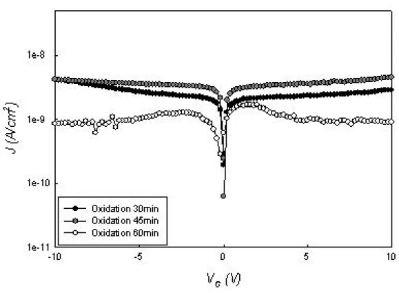
(49) quality of the control oxide. The electrical I-V characteristics were measured by Keithely 4200 Precision Semiconductor Parameter Analyzer. Then, secondary ion mass spectroscopy (SIMS), as material analyses, was also measured. The SIMS result was used to analyze the depth of elements. Besides, the electron spectroscopy for chemical analysis (ESCA) had been taken to analyze both elemental and chemical bonding information about the material comprising the sample surface.. 3.3 Results and Discussion Fig. 3-2 shows the capacitance-voltage (C-V) hysteresis of the structure I with three different conditions in oxidation duration. In 30 minutes short term oxidation, shown in Fig. 3-2(a), it has an obvious large memory window of ~4.7V under ±5V C-V sweeping. Also, the memory window is of ~3.6V under ±5V C-V sweeping for the MOIOS structure after 45 minutes oxidation, as shown in Fig. 3-2(b). As the oxidation duration increasing, its threshold-voltage shift (ΔVTH, just as memory window) becomes smaller reversely. This is because the nucleated tungsten elements as charge-trapping centers would be oxidized to dielectrics (tungsten oxide, WOx). Hence, long oxidation duration causes decreased memory ability resulted from the over oxidation of W-NCs. As the dry oxidation duration extended to 60 minutes, the memory window of ~3.2V under ±5V C-V sweeping had already decreased up to thirty percent compared with 30 minutes dry oxidation, shown in Fig. 3-2(c). In addition, the electrical current-voltage (I-V) hysteresis of three conditions in oxidation duration of the structure I is shown in Fig. 3-3. With the extension of oxidation duration from 30 minutes to 60 minutes, the leakage current exhibited a nearly result about from 10-8 order to 10-9 order. It is torrent for carrier stored in charge trapping layer. 31.
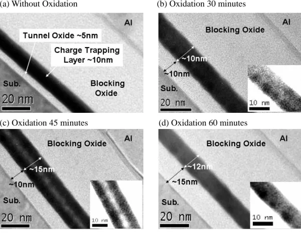
(50) Fig. 3-4 (a) ~(d) showed the transmission electron microscope (TEM) diagrams of the structure I for the sample without oxidation and with dry oxidation duration for 30, 45 and 60 minutes, respectively. By contrast, Fig. 3-4(a) obviously showed the thickness of tunnel oxide layer and charge trapping layer were closed on their initial deposited conditions as 5nm and 10nm, respectively. It is found that the tunnel oxide layer and charge trapping layer are both become thicker obviously and extended outward, especially the tunnel oxide extended in thickness about 2~3 times. It is considered that the tungsten elements were out-diffused during thermal oxidation in furnace. In the process of oxidation by furnace, we kept the furnace at 900℃ for 10 minutes in N2 ambient to stabilize the temperature before oxidation. So the tungsten elements could be get energy to out-diffused, usually tended upward because of the hotter blocking oxide film. The other study also indicated that tungsten tended to exist in silicon oxide not in silicon film [3.6]. As tungsten elements diffused, the original deposited W5Si3 film would be left as Si-rich tungsten silicide film or even as poly-Si layer. Furthermore, the thermal anneal procedure in nitrogen ambient causes the tungsten silicide agglomerated [3.7]. The high diffusivity for oxygen in grain boundary contributes the thicker inner-oxide formation. Hence, as the oxidation proceeded, the poly-Si layer would be oxidized as charge trapping layer. For the oxidized W5Si3 trapping layer, stayed Si elements in charge trapping layer were oxidized to form silicon oxide. However, there is no obvious difference of thickness for thicker tunnel oxide verse oxidation duration. It is again evidenced that the increased tunnel oxide is contributed by the initial W5Si3 layer out diffusion in nitrogen ambient, and then oxidized by sequent diffused oxygen. However, the main difference for different oxidation duration is the trapping layer formation which will be discussed in the next section.. 32.
(51) The nanocrystals (the charge storage layer) embedded in dielectrics layer of metal-oxide–insulator-oxide silicon (MOIOS) memory device was utilized to capture the injected carriers from the channel, which caused a variation in the threshold voltage of the memory device. The bidirectional C-V sweeps were performed from deep inversion to deep accumulation and in reverse, which exhibits an electron charging effect. When the device was programmed, the electrons directly tunneled from the Si substrate through the tunnel oxide by Fowler-Nordheim (F-N) tunneling and they were trapped in the charge storage layer. For the erasion, the holes might tunnel from the valence band of the Si substrate and recombined with the electrons trapped in the charge storage layer, or the electrons tunnel back to the Si substrate from the charge storage layer. The control oxide was utilized to prevent the carriers injecting into the charge trapping layer by Fowler-Nordheim (F-N) tunneling from gate electrode. Figure 3-5 shows the proposed mechanism of structure I during thermal oxidation in furnace. For 30 minutes oxidation, the tungsten elements have already nucleated near tunnel oxide as shown in Fig. 3-4(b). It is considered that tungsten nanocrystals nucleated near tunnel oxide as shown in 30 minutes oxidation. Then, obvious a lighter region inside the charge trapping layer for 45 minutes. The other arrangement of dots from tungsten segregated near blocking oxide compared to 30 minutes oxidation. As the previous paragraph described, W elements tended to out-diffuse. The left Si elements in initial tungsten silicide layer will be oxidized as the thicker tunnel oxide. However, the diffused W element to the capped oxide causes the lower W/Si ratio. As a result of lower W/Si ratio value, the oxidation behavior at the capped oxide is not the same as the pure W5Si3 [3.5]. For the lower W/Si ratio, such as WSi2, exposed to oxygen at high temperatures, the oxidation behavior is divided to two sequential reactions according to Equations. (3-1) and (3-2): 33.
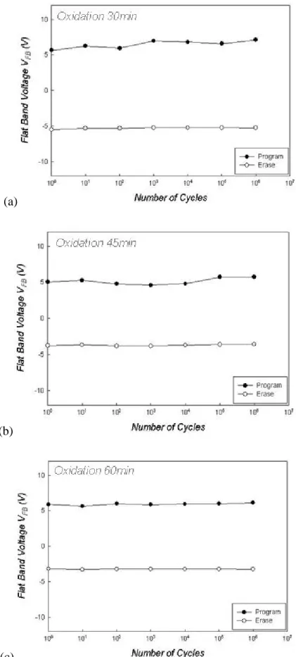
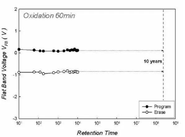
(52) 5WSi2(s) + 7O2(g) → W5Si3(s) + 7SiO2(s). (3-1). W5Si3(s) + (21/2)O2(g) → 5WO3(s or g) + 3SiO2(s). (3-2). Therefore, the Si-rich tungsten silicide would be oxidized to first form W-rich tungsten silicide and then oxidized to tungsten oxide. It could be suggested that the upper part of tungsten silicide film near blocking oxide was oxidized as above oxidative behavior. The reducible part tended to form W5Si3 and nucleated continuously near the blocking oxide layer as shown in Fig. 3-4(c). In addition, the center region of charge trapping layer would be the silicon oxide which oxidized from remained silicon elements after tungsten elements nucleated. Moreover, the phenomena of separated charge trapping layer is disappear for 60 minutes oxidation. The over-oxidation causes the upper tungsten-silicide layer completely oxidized. Even, the intermediate layer in the charge trapping layer occurred for 45 minutes oxidation will again let W element inter-diffusion. However, the sizes of W-NCs at the interface of tunnel oxide are increasing for prolonged nucleation, shown in Fig. 3-4(d). Finally, Fig. 3-6 and Fig. 3-7 showed the electrical reliability characteristics of structure I. The endurance characteristics of three oxidative conditions in structure I all showed in Fig. 3-6 (a)~(c) which indicates the memory window can be distinguished after 106 program/erase cycles at room temperature. As shown in Fig. 3-7, the charge retention characteristics of structure I after 60 minutes oxidation estimated by C-t measurements at room temperature [3.8]. It also indicated that the carrier charges could be kept until 104 seconds, leading to a good memory characteristic.. 34.
(53) 3.4 Conclusions Tungsten nanocrystals embedded in SiO2 had been fabricated with appropriate control of the process temperature and oxidation time. As the W5Si3 film oxidized at 900°C in thermal furnace, the thickness of tunnel oxide are thicker due to W element out-diffusion, the fast oxygen diffusion path in grain boundary of annealed tungsten-silicide layer. The main difference of oxidation duration is the formation of charge trapping layer. The significant C-V hysteresis of voltage shifts of 4.7V~3.2V were observed at ±5V sweep voltage. The good electrical reliability characteristics, such as retention time and endurance, can be also realized in the proposed structure in this work. The ease technology for W-NCs formation is suitable for the current nonvolatile memory device manufacture.. 35.
(54) Figure 3-1 The process flow of structure I in this work.. 36.
(55) (a). (b). (c) Figure 3-2 The C-V hystereses of structure I with (a) oxidation 30 minutes (b) oxidation 45 minutes and (c) oxidation 60 minutes. 37.
(56) Figure 3-3 The I-V characteristics of structure I with oxidation 30 minutes, oxidation 45 minutes and oxidation 60 minutes, respectively.. 38.
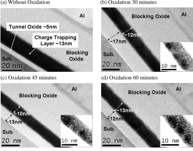
(57) (a) Without Oxidation. (b) Oxidation 30 minutes. (c) Oxidation 45 minutes. (d) Oxidation 60 minutes. Figure 3-4 Transmission electron microscopy (TEM) analysis of structure I (a) without oxidation, (b) with oxidation 30 minutes, (c) with oxidation 45 minutes and (d) with oxidation 60 minutes, respectively. The insert is the TEM analysis by adjusting contrast.. 39.
(58) Figure 3-5 The mechanism of structure I during thermal oxidation in furnace.. 40.
(59) (a). (b). (c) Figure 3-6 The endurance characteristics after different write/erase cycles of structure I with (a) oxidation 30 minutes (b) oxidation 45 minutes and (c) oxidation 60 minutes. 41.
(60) Figure 3-7 The charge retention characteristic of structure I with 60 minutes thermal oxidation.. 42.
(61) Chapter 4. Application of Oxygen/Nitrogen-Incorporated W-NCs NVMs. 4.1 Motivation In previous section, the memory effect and the electrical reliability for tungsten nanocrystals surrounded in dielectrics by oxidizing sputtered tungsten-silicide (W5Si3) layer were also investigated. In this contribution, the carrier gases like oxygen or nitrogen were added as the tungsten silicide deposition. The non-reacted gases change the composition of W/Si ratio (WSiO/WSiN) and the composition of as-deposited tungsten-silicide layer (WSiN), which affect the memory effect. Also, the effects such as the W element out-diffusion, thicker inner-oxidation formation, and charge trapping layer formation, are discussed in this section. Furthermore, the electrical reliability characteristics were also performed.. 4.2 Experiment Procedures Figure 4-1 (a) and (b) showed the schematic diagram of fabricating procedures labeled as structure II and structure III, in this thesis. First, single-crystal 6 inch (100) oriented p-type silicon wafers were chemically cleaned by standard RCA clean. The wafers were followed by a thermal oxidation process to form 5-nm-thick dry SiO2 layer as a tunnel oxide in an atmospheric pressure chemical vapor deposition 43.
(62) (APCVD) furnace. Then, a 10-nm-thick tungsten-rich tungsten silicide (W5Si3) thin film was deposited onto the tunnel oxide by sputtering system (the same as Structure I). Simultaneously, the carrier gas, such as O2 (labeled as Structure II) and N2 (labeled as Structure III), were also added in the cavity of sputtering system as the tungsten silicide deposition at room temperature. The oxygen-incorporated W5Si3 (WSiO) film in structure II is deposited using mixed-flow. of. O2. 2sccm/. Ar. 24sccm.. Also,. in. structure. III,. the. nitrogen-incorporated-W5Si3 (WSiN) film was sputtered in mixed-flow of N2 10sccm/ Ar 24sccm. Subsequently, a 20-nm-thick SiO2 was deposited by plasma enhanced chemical vapor deposition (PECVD) system. Then, the high temperature thermal oxidation was performed in the thermal furnace in oxygen ambient for 30, 45, and 60 minutes. Afterward, a 30-nm-thick SiO2 was deposited by PECVD system to form a thicker control oxide layer. Finally, the Al gate electrode was patterned and sintered to form a metal-oxide-silicon (MOS) structure. The MOIOS structures with W-NCs embedded dielectric layers as charge trapping centers were fabricated and investigated. The micro-structures of samples were analyzed by transmission electron microscope (TEM) analysis. The capacitance-voltage (C-V) characteristics were measured at frequency 100 kHz by HP4284 Precision LCR Meter and this measurement analyzed the memory effect of nanocrystal memories and electrical characteristics. However, the current-voltage (I-V) measurements showed the leakage current to verify the quality of the control oxide. The electrical I-V characteristics were measured by Keithely 4200 Precision Semiconductor Parameter Analyzer. The material analyses, such as secondary ion mass spectroscopy (SIMS), and electron spectroscopy for chemical analysis (ESCA), were also performed in this section.. 44.
(63) 4.3 Results and Discussion The bidirectional C-V sweeps were performed from deep inversion to deep accumulation and in reverse, which exhibited an electron charging effect. The nanocrystals (the charge storage layer) embedded in dielectrics layer of metal-oxide–insulator-oxide silicon (MOIOS) memory device was utilized to capture the injected carriers from the channel, which caused a variation in the threshold voltage of the memory device. Fig. 4-2 showed the capacitance-voltage (C-V) hysteresis of the structure II (sputtered W5Si3 layer in Ar/O2 ambient) with oxidation duration from 30 minutes to 60 minutes. In 30 minutes short term oxidation, the memory window was ~3.9V under ±5V C-V sweeping shown in Fig. 4-2 (a). However, in structure II, the threshold voltage shifts as the dry oxidation duration increasing were not obviously different. It is suggested that the oxygen elements existed in dielectrics in structure II more than the contents in structure I, the oxidative rates tended to improve in structure II as 30 minutes oxidation. Therefore, with the extension of oxidative time from 45 minutes to 60 minutes, these samples have already similar ratios of the tungsten elements oxidized into tungsten oxide. Hence, it is found that the memory windows were ~3.0V and ~3.1V under ±5V C-V sweeping for 45 minutes and 60 minutes dry oxidation were shown in Fig. 4-2 (b)and (c), respectively. In addition, the electrical current-voltage (I-V) hysteresis of three conditions of oxidation duration for the structure II was shown in Fig. 4-3.. It is found that similar results to the I-V. diagram in structure I as discussed in Chap 3. The leakage currents are between 10-8 order and 10-9 order for 30~60 minutes dry oxidation. Fig. 4-4 (a) ~(d) show the transmission electron microscope (TEM) diagrams of the structure II for the sample without oxidation and with dry oxidation duration for 45.
(64) 30, 45 and 60 minutes, respectively. It is considered that the tungsten nanocrystals segregated downward until they reach the tunnel oxide surface during thermal oxidation in furnace. In the same way, it is found that the tunnel oxides are also thicker after three kinds of thermal oxidation duration. However, the double-layer nanocrystals were not found after thermal oxidation as shown in the TEM diagrams of structure II. It is considered that the tungsten elements more tended to embedded in SiO2 than in Si [4.1]. However, the oxygen-incorporated W5Si3 layer has the similar component compared to the capped oxide. Hence, the W elements were almost uniform after thermal annealing in nitrogen ambient. The tungsten elements were not upward diffused seriously and not segregated without another tungsten nanocrystal arrangement near the blocking oxide layer. In addition, it also suggested that the additional oxygen radical elements adding from charge trapping layer deposition would cause the increased oxidation rate. Hence, the TEM diagram for 30 minutes dry oxidation was similar to the case of oxidation over 45 minutes in structure I. Moreover, due to the raising oxidation rate, the charge storage units can be oxidized more in the same oxidation condition which was performed on structure I. It is mentioned that the decreased memory characteristics as former. The proposed mechanism of structure II during thermal oxidation in furnace was showed in Fig. 4-5. In addition, the electrical reliability tests of structure II would be shown in Fig. 4-6 and Fig. 4-7. In Fig. 4-6 (a)~(c), the endurance characteristics of structure II after three oxidation conditions indicate the memory window can be retained after 106 program/erase cycles at room temperature. In addition, Fig. 4-7 exhibits the charge retention characteristics of structure II after 60 minutes oxidation estimated by C-t measurements at room temperature. It is found that the carrier charges can be kept after 104 seconds. The good electrical reliability characteristics were also obtained in the proposed structure II. 46.
數據
+7

Outline
Nanocrystal Nonvolatile Memory Devices
Results and Discussion
Application of Oxygen/Nitrogen-Incorporated W-NCs NVMs
ESCA Analyses of W-NCs Embedded in Dielectric Layers
Effect of Capped Oxide for W-NCs Formation in Dielectric Layers Dielectric Layers
Discussions of Non-ideal C-V Hysteresis of W-NCs Nonvolatile Memory
Future Work
相關文件
First, Henry showed me the best cubic pastry shop in Chiayi.. We tried different flavors of
下列哪一種記憶體屬於非揮發性記憶體, 不會因電源關閉而使其中的資料消 失, 但是可以透過電壓的方式重複抹除資料, 可用於基本輸入/ 輸出系統 (Basic Input / Output System,BIOS)
In fact, his teachers believe that it is his good ear for music that has helped him with the precise pronunciation of different languages – especially with a tonal language like
using tungsten single crystal emitters the thermally-assisted Schottky type, using emitters of zirconium oxide. field emission
In order to identify the best nanoparticle synthesis method, we compared the UV-vis spectroscopy spectrums of silver nanoparticles synthesized in four different green
In order to use the solar rays more efficient and improve the conversion efficiency of solar cell, it is necessary to use antireflection layer to reduce the losses of
We found that there were different on sample’s DCP penetration curves that conduced by its kind of soils, maximum granular diameter, coarse aggregate content, it showed up
為了改善唯讀記憶體無法寫入資料的限制,電腦廠商研發出數種除了「讀」還可 以「寫」的 ROM ,其中以 快閃記憶體 ( flash
