應用於物聯網系統之感測器與類比至數位轉換器之研製
29
0
0
全文
(2) 中 文 摘 要 : 物聯網被視為全球下一波最具成長潛力的應用,近年來台灣也著手 積極研發相關技術。然而,我國物聯網技術向來著重於網路層與應 用層,顯少著墨於感測層。基於此,本計畫擬以三年(2017 年8 月 1日至2020 年7 月31 日)的時間以半導體製程、針對應用於物聯網 的類比至數位轉換器進行深入之研究,以厚實感測介面電路之自主 研發能力。本計畫第一年將開發合適的架構與電路設計技術,並著 手研製雛型晶片。第二年的研究重點將著重於驗證雛型晶片,進行 架構調整與電路優化的設計,並研製完整的類比至數位轉換器晶片 。第三年的研究重點將放在感測器與類比至數位轉換器整合與量測 驗證。 中 文 關 鍵 詞 : 類比至數位轉換器、物聯網、低功耗。 英 文 摘 要 : Internet of Things (IoT) is being labelled as the next big thing in the world. Developing key techniques for IoT applications has gained a lot of popularity in Taiwan recently. However, most of them focus the attention on application and network layers. Development of the sensor layer is relatively rare. Accordingly, this project is proposed to investigate the IC design techniques for sensors and analog-to-digital converters for IoT applications. It will be carried out in three years (from August 1, 2017 to July 31, 2020). The main objective of this project is to build a foundation in reinforcing the capability of independent research and development for sensor/ADC design. In the first year, we will develop proper structure and circuit design techniques. Several proof-of concept prototypes will be carried out during this stage. In the second year, we will focus on verifying the prototypes, refining the designs and tape out the complete chips. In the last year, we will focus on the integration of the sensors and ADCs. The whole system will be verified by physical prototype measurement. 英 文 關 鍵 詞 : Analog-to-digital converter, Internet of things, Low power consumption..
(3) 科技部補助專題研究計畫成果報告 (□期中進度報告/■期末報告). 應用於物聯網系統之感測器與類比至數位轉換器之研製 Research on Design Techniques for Sensor and Analog-to-Digital Converter in IoT Systems. 計畫類別:■個別型計畫 □整合型計畫 計畫編號:MOST 106-2221-E-006-238-MY3 執行期間:106 年 8 月 1 日至 107 年 7 月 31 日 執行機構及系所:成功大學電機系 計畫主持人:張順志 計畫參與人員:胡桓睿、寸恩澤、吳皓昇、曾華安、李嘉銓、馬兆賢 本計畫除繳交成果報告外,另含下列出國報告,共 1 份: □執行國際合作與移地研究心得報告 ■出席國際學術會議心得報告 □出國參訪及考察心得報告. 中. 華. 民. 國 107 年 10 月 31 日 1.
(4) 一、前言 由於半導體技術幾十年來的進展,使得電子產品的通訊速度與運算能力大幅提升,進一步促使物 聯網(Internet of Things;IoT)的出現。其中透過由眾多感測器(Sensor)所組成的感測網路(Sensor Network) 更是物聯網裡不可或缺的元素。透過感測網路,由感測器偵測環境中的各種狀況,如溫度、濕度與影 像等等,經由處理單位(Processing Unit)進行基本的運算處理,再由傳輸單位(Transmission Unit)將資料 傳遞給網路中的其他感測器與無線資料收集器(Wireless Data Collector),進行物聯網的溝通。近年來在 許多市場報告與觀察中,我們可以得知將物聯網引入各領域儼然成為一種趨勢,包括汽車產業中的先 進駕駛輔助系統(Advanced Driver Assistance Systems;ADAS)與自動駕駛(Autonomous Vehicle)、生活中 的智能家居(Smart House)甚至是智能城市(Smart City)等等。為確保上述應用的可靠度與安全性,感測 器的靈敏度和其由類比轉換成數位訊號之正確性便是實現物聯網系統可靠度與安全性的第一道關鍵。. 二、研究目的 基於上述之背景,本研究計畫提出以 CMOS 製程研製類比至數位轉換器(ADC)來輔助物聯網系統 提升可靠度與安全性,因此擬研發之電路必須要更加精確、穩定與耐用。為此,除了傳統低功耗的設 計目標外,本研究計畫將致力於提升感測器與 ADC 精確度,亦將著眼於開發抗環境變異(電源電壓不 穩定)影響的電路設計技術。此外、針對多感測節點(例如:家用或車用)訊號處理的應用,其訊好轉換 的方法可改分為二:其一是採用多個低速 ADC,其二是開發一個高速 ADC 以時序分工方式提供多個 感測器使用。於此研究計畫,上述兩種方式皆為我們研究探討的議題,因此除了開發低速低耗能的 ADC 外,吾人亦研發高速低耗能 ADC。本計畫預期經由三年的研究期程,將逐步發展一個應用於物聯網系 統之類比前端子系統。接下來在文獻探討與研究方法、結果討論等章節將依照上述研究重點分別加以 詳細說明。. 三、文獻探討 承續研究目的所述,本子計畫過去一年針對高精確度低功耗、抗電源電壓不穩定、高速低耗能之 連續漸進逼近式類比至數位轉換器進行深入的研究,因此以下分別針對與這三個子題相關的文獻與已 知的研究成果加以深入探討並整理如下: 電容不匹配(mismatch)與比較器精確度,是限制高解析 SAR ADC 效能的主要兩個原因。在製程廠 元件限制下,電容線性度飄移使大部分 SAR ADC 在考量電容負載及功耗後所選定的電容值,其解析 度規格與效能限制在十位元;另一方面,當解析度要求提高,雜訊的影響成為關鍵,尤其在先進製程 中,操作於低電壓環境下,設計高精確度的比較器難度提升,往往需要付出功耗及速度的代價。 近年來許多團隊提出不同的方法解決非理想效應,以提高 SAR ADC 的解析度及效能。為了改善 電容的線性度並維持電容負載的大小,主要可以透過電容平均交換(Capacitor Swapping Average)或數 位校正(Digital Calibration)的方式[1][2][3][4][5]。而在雜訊部分,也有研究針對架構探討以減輕比較器 的設計負擔,例如殘值放大(Residue Amplify)、超取樣(Oversampling)和雜訊整形(Noise Shaping)等技 巧[5][6][7][8][9][10]。 在這些多元的解法之中,除了考慮到其技巧的功效之外,也需要將其實現電路的複雜度以及對應 的功耗納入考量。假如我們以不使用複雜與耗成本的技巧為前提,發展出增進解析度的技術,將可以 使我們的感測系統更加完整且實用,並有機會發展至產品端。 除此之外,逐漸趨近式類比數位轉換器(SAR ADC)優異的能源轉換效率(energy- efficiency)雖然眾 所皆知,但是大部分的文獻都未將其周邊電路的的能源消耗考慮進去,例如參考電源緩衝器(reference buffer),其功耗常常遠高於 SAR ADC 本身好幾倍[11],可能將不利於 SAR ADC 在物聯網的發展。 SAR ADC 在量化(quantization)的過程中,會根據前一次比較結果切換電容陣列來產生下一個比較 2.
(5) 基準,因此會不斷對參考電源抽載電流,造成比較時參考電源不精準的問題。 針對此一問題,吾人設計了一個不需要輸出端大電容的參考電源穩壓器,大大節省了晶片中所需 要的額外電容。另外,藉由非二元搜尋演算法[12] [13] (the Nonbinary Algorithm)容忍參考電源的錯誤, 大幅地降低了該穩壓器的頻寬需求,因此功率消耗也大大降低。. 四、研究方法、結果與討論 以下分別就過去一年來針對高精確度低功耗、抗電源電壓不穩定、高速低耗能之 SAR ADC 三個 子題的研究方法與結果說明如下: (1) 高解析低功耗之逐漸逼近式類比數位轉換器 (1-A) 研究方法: 本團隊發表於 2018 TCAS-I 的逐漸逼近式類比至數位轉換器[14],利用殘值超取樣技術(Residue Oversampling),可以不需要複雜的校正電路即可增加類比數位轉換器的精確度,但因需額外的比較次 數故操作速度有其極限。另一方面,單通道類比至數位轉換器因為製程等因素其速度面臨提升瓶頸, 使得能藉由通道數增加而加速的多通道時序交錯式類比至數位轉換器愈來愈受歡迎。再者,多通道時 序交錯式類比至數位轉換器的動態功耗並不會隨著速度提升而倍數增長。但其缺點為失調失配(offset mismatch)、增益失配(gain mismatch)、時序歪斜(timing mismatch)、線性度失配(linearity mismatch)等 非理想效應會嚴重影響多通道時序交錯式類比至數位轉換器的效能。 因此若將殘值超取樣技術結合多通道時序交錯的架構,不僅可以提升整體 ADC 的操作速度,在殘 值超取樣 SAR ADC 擁有良好精確度的前提下,又可以減輕各通道之間增益失配、失調失配、線性度 失配的校正負擔。而在時序歪斜方面,本團隊提出一個低時脈偏移的取樣電路,故此多通道時序交錯 式類比至數位轉換器不需額外的校正電路。 此十二位元時序交錯式殘值超取樣逐漸逼近式類比至數位轉換器的架構圖,將單通道的殘值超取 樣 SAR ADC,組成四通道時序交錯的 SAR ADC,其架構圖如圖一。其中單通道 SAR ADC 主要使用 本團隊提出的「殘值超取樣技術」,而為了解決電容之間錯誤量,我們使用「二進制的錯誤補償機制 ( Binary - Scaled Error Compensation Method )[15]」加大能解的電壓範圍以涵蓋錯誤量。而電容的切換 方法採用「Merged capacitor switching[16]」結合「單調式( Monotonic[17] )」電容切換機制,簡單來說 最後一次切換只切了 0.5Vref 的電壓,使得電容陣列的複雜度降低一個位元。. 圖一、十二位元時序交錯式殘值超取樣逐漸逼近式類比至數位轉換器的架構圖. (1-B) 結果與討論: 接下來為利用 Matlab 軟體模擬的結果。Matlab 的模擬環境為:理想的 SAR ADC,唯一的非理想 變數為電容的不匹配,每個單位電容都分別加大標準差為 0.03 的 mismatch,且單位電容之間並無相 關性。下面分別顯示單通道及多通道使用 Mixed Switching Method[18]的切換方式,不使用殘值超取樣 技術(ROSR=1)、殘值超取樣兩次(ROSR=2)、殘值超取樣四次(ROSR=4)分別的 100 次模擬 INL 疊圖。 3.
(6) 可以明顯看到,使用殘值超取樣技術能有效提升 INL,而四通道又比單通道改善更多。 單通道. 四通道. 考慮時序歪斜將會嚴重影響多通道 SAR ADC 的整體效能,本團隊提出一個改良的拔靴式取樣電 路(Bootstrapped Switch),在傳統的拔靴式取樣電路內加入一顆 NMOS 電晶體,控制四通道的取樣結 束時間皆由最主要的取樣時脈(Clks_master)控制,能有效改善時脈歪斜的情形,其電路圖如圖二,而 時脈關係圖如圖三。 Clks_master. M3 M4. Clks_div i. M8. M1. M2. Cs M10. M7. M5. M9 MS. Vip. Clks_div i. Vop. Vin. M6. MD. 圖二、改良的拔靴式取樣電路. 250p. 250p 250p 750p 750p. ФФ Clks_master. Ф. Clks_div Ф1 Ф11. Ф1. Clks_div Ф2 Ф22. Ф2. Ф3 Ф33 Clks_div. Ф3. Clks_div Ф4 Ф44. Ф4. 750p. 圖三、四通道時脈關係圖. 表一為此十二位元四通道時序交錯式殘值超取樣 SAR ADC 佈局前(Pre-Simulation)及佈局後模擬 (Post-Simulation)的規格列表。 4.
(7) 表一、Post-simulation 規格列表. 規格 使用製程 Resolution (bit) Supply Voltage ( V ) Sampling Frequency ( MS/s ) Input Frequency ( MHz ) ENOB (bit) Power (mW) Core Area ( mm2 ) Chip Area ( mm2 ) FOM ( fJ / conv.-step). 佈局前模擬 90 nm 12 1.0 80 36.25 11.93 1.03 N/A N/A 3.6. 佈局後模擬 90 nm 12 1.0 50 22.66 10.95 2.52 0.0313 1.0416 28.1. (2) 抗電源電壓不穩定之SAR ADC: (2-A) 研究方法: 我們目前所設計的電路架構(圖一),是一個 11 位元非二元權重的 SAR ADC 加上一個參考電源的 穩壓器。(表一)為該 SAR ADC 的電容權重及其分配的容忍量。 AVd d. AVd d2. C 12 /2. C 11 /2. C 10 /2. C 9 /2. C 12 /2. C 11 /2. C 10 /2. C 9 /2. C8. DVdd. ….. C1. C0. Vip. Vre fp. Dire c ts witch ing Co ntrolle r. Re fe re nce Re gula tor. Vre fn. C 12 /2. C 11 /2. C 10 /2. C 9 /2. C 12 /2. C 11 /2. C 10 /2. C 9 /2. Diffe re ntia l La tch. 13. DE C. 11. C om pa ra tor C ontrolle r. Vin C8. ….. C1. C0. 圖四、電路架構圖 表二、電容權重及其容忍量 位元循環編號:. 1. 2. 3. 4. 5. 6. 7. 8. 9. 10. 11. 12. 電容權重. 512. 128. 128. 112. 64. 36. 20. 11. 6. 3. 2. 1. 容忍量( LSB). 0. 256. 128. 32. 16. 8. 4. 2. 1. 1. 0. 0. 13. 0. 在我們的模擬中發現,摺疊電壓隨耦器(FVF; Flipped Voltage Follower)[19]比 NMOS 源極隨耦器 (NSF; NMOS Source Follower) [11][13]在驅動 SAR ADC 時還要可靠,因為其在後面位元的穩壓效果 較好(圖五)。後面位元因為通常難以分配容忍量,而且更敏感於參考電源錯誤,所以參考電源在 ADC 解到最後時必須穩定回來。. 5.
(8) 圖五、NSF 和 FVF 驅動 SAR ADC 的參考電壓暫態響應 圖六是我們設計的參考電源穩壓器的電路圖。我們主要採用 FVF 的架構,因為它只需要幾個電晶 體,就能形成一個低壓差穩壓器(LDO; low-dropout regulator)[20][21],這樣能讓電路中的極點(pole) 分布簡單,暫態響應也能快速點。我們將主極點設計在 Vf 而非在 Vrefp,因為前者相對後者而言看 到的阻值較大,若以 Vrefp 為主極點,則需要一個超大電容來使 LDO 穩定。此外,我們加了 Msw 這顆電晶體,除了讓開迴路增益(open-loop gain)再大一點,因為 Vf 的等效電阻更大了,就不需要太 大的 Cc1 來使系統穩定。 Control Volta ge Ge ne ra to r. S ingle -Tra ns is tor-Control LDO Avdd 2. M4. M3. Mp2. Mp. Vre fp MR2. Cc 2. Vctrl. Mc2. Mc CB. M1. Vb. M2. Mb3. VBG. Vf. Ms w. Ms w2. Mb. MR1. Mb2 Cc 1. 圖六、參考電源穩壓器的電路圖 (2-B) 結果與討論: 模擬出來的開迴路增益、增益帶寬積(gain-bandwidth product)、相位邊限(phase margin)、總工作電流、 總靜態功耗分別為 57 dB, 234.16 MHz、57°、894 µA 及 1.6 mW。加上棒線模型和 ADC 模擬後的快 速傅立葉轉換(FFT; Fast Fourier Transform)頻譜圖如(圖七)所示,SNDR 為 67.61 dB,換算而得的 ENOB 為 10.94。. 圖七、256 點的快速傅立葉轉換頻譜圖. 6.
(9) (3) 高速低耗能之SAR ADC: (3-A) 研究方法: 於此研究子題吾人採用了全域時序的取樣電路架構進行通道選取的概念,並改善原先的取樣電路 來增強全域時序對於子域時序的影響力,進而使得造成取樣間隔不匹配的路徑盡可能減少,在這樣的 架構下,即使不使用額外的校正電路,在消除取樣間隔的不匹配也可以達到很好的效果;而為了讓單 通道達到較高的操作速度,使用了子範圍類比數位轉換器(sub-range ADC)的架構,以一個副(coarse) SAR ADC 對應兩個主(fine) SAR ADC 形成雙通道,為了讓子轉換器的操作速度可以是主轉換器的兩 倍,採用了循環展開(loop-unrolling)的比較器架構,以忽略比較器重置時間(comparator reset time)所造 成的浪費,並且使用非二進制演算法(non-binary algorithm)的電容陣列來容忍前兩者所產生出的錯誤, 其架構如圖八。 Coarse ADC. Clks_Global. 64C. 32C. 16C. 16C. 64C. 32C. 16C. 16C. Coarse SAR Logic. Loop-unrolled. VREF GND. VREF GND. VREF GND. Clks_Global. 240C. 120C. 120C. 60C. 60C. 30C. 30C. 30C. 30C. 16C. 16C. 8C. 8C. 4C. 2C. 4C. 2C. C. C. C. C. Fine SAR Logic. 240C. Vip Vin VREF GND. Time-interleaving Logic. Channel 2 Channel 1. 10. Fine ADC. 圖八、整體架構圖 . 全域時序取樣電路改良 原先傳統的取樣電路中,放電路徑 M1 的閘極接至各通道的子時序(這邊以 Clk_ch_i 表示),使得取. 樣間隔會隨著各通道間子時序的不匹配而有所差異,進而造成效能下降,在[22][23][24]中,將 M1 改 接至全域時序(Clk_Global),如圖九所示,使得各通道間取樣的間隔取決於全域時序,讓子時序間不匹 配的影響減少,如圖十。. (a)傳統取樣電路. (b)全域時序取樣電路 圖九、取樣電路. Clks_Global. Clks_ch_1. Skew. Clks_ch_2. 圖十、子時序不匹配造成的取樣漂移 7.
(10) 全域時序操作的概念在於,當取樣電路中 M2 與 M1 這條放電路徑導通時,會將負責取樣的 MS 關閉,此時取樣電路從 track phase 進入到 hold phase,換句話說,取樣間隔的時間點是透過 Clk 的負緣 所決定,若我們將放電路徑的控制訊號,從原本各通道的子時序換成全域時序來處發的話,即可使得 各通道的取樣時間點對應起來。 本晶片延續這樣的概念,除了原先全域時序的取樣電路外,額外增加了 M10 的路徑(圖十一)來改 善全域時序在取樣電路內的影響力。原先當放電路徑導通時,因為部分的電路仍由子時序控制著,使 得 M4 的路徑並不會關閉,形成放電路徑在對於取樣開關 MS 的閘極放電的同時,M4 的路徑仍會對該 點進行充電,彼此之間相互拉扯,而增加 M10 的功能則在於當放電路徑導通時,會盡量使 M4 的路徑 關閉,確保取樣時間點的穩定不受到子時序的干擾,除了可以增加取樣時的效能外,並減少取將間隔 的不匹配效應。. (a)改良後 (b)操作概念 圖十一、改良後的全域時序取樣電路與其概念 . 高速的單通道 SAR ADC 子範圍類比至數位轉換器(Sub-range)架構 先前提到限制 SAR ADC 速度的原因有兩個,分別是 DAC settling time 與比較器的操作速度。其中 DAC settling time 所造成的影響,以 MSB 最為顯著,因為 SAR ADC 的電容陣列為二進制,負責 MSB (Most Significant Bit)電壓切換的電容會較後面 LSB(Least Significant Bit)的電容來得大,所需要的 settling 時間也多上許多,為了突破這樣的限制,本晶片採用類似於[25][26][27]中的 Sub-range 架構(圖 十二為示意圖),將前面四個 MSB 的部分交由 Coarse SAR ADC 來負責,一方面 Coarse SAR ADC 的 DAC 可以比 Fine SAR ADC 來的小很多,因此大大減少了 DAC settling 所需要的時間;此外 Coarse SAR ADC 中的比較器設計上也可以更著重在速度方面,提高了前面幾個 MSB 時的比較速度,而需要精確 的部分則交由 Fine SAR ADC 中的比較器來負責,此一概念類似於雙模式比較器(two mode comparator) 的架構[28]。 這些原因使得 Coarse SAR ADC 在速度上可以遠遠高於 Fine SAR ADC,並且當 Coarse SAR ADC 在進行解析的同時,已經解析出的前幾個 MSB 也可以提早讓 Fine SAR ADC 中的 DAC 進行電壓切換, 解決了原本 Fine DAC settling 需要大量時間的瓶頸(如圖十二的時序圖),讓前面幾個 cycle 的速度可以 完全取決於 Coarse SAR ADC。也就是說,當 Coarse SAR ADC 操作的速度越快,整體 SAR ADC 的速 度也會越快,而最理想的狀況是,當 Coarse SAR ADC 的速度可以是後端 Fine SAR ADC 的兩倍時,則 可以實現以一個 Coarse SAR ADC 對應雙通道的 Fine SAR ADC,來實踐高速少通道的 Time-interleave SAR ADC。 為了達到這樣的想法,我們勢必要加快原本 Coarse SAR ADC 的架構。. 8.
(11) Coarse ADC MSB. MSB-1. MSB-2. MSB-3. Standby MSB MSB-1 MSB-2 MSB-3. Fine ADC. Tcomparison. Tsettle. Tstandby. 圖十二、子範圍架構示意圖與其操作時序圖 循環展開(loop-unrolling)比較器架構 透過前面提到的 Sub-range 架構,Coarse SAR ADC 的 DAC 已經較 Fine ADC 的 DAC 小很多,所 以 DAC settling 並不會是造成 Coarse SAR ADC 速度限制的原因,所以主要的限制來自於比較器:每個 比較器有兩個階段,分別是比較階段(compare phase)與重置階段(reset phase)。因為 DAC settling 所需的 時間已經小於比較器重置時間,所以此時重置階段需要的時間會是拖累操作速度的主因,為了解決這 個問題,我們使用循環展開[29][30]的比較器架構,亦即在一個 N-bit SAR ADC 中使用 N 個比較器,使 得在解析的過程中,並不需要重置比較器,而是直接使用下一個在循環中仍未使用過的比較器,當 ADC 完成一次完整的接析後,再統一一次重置,讓我們並不需要考慮比較器重置時間對於速度上的影響, 如同圖十三,使得 Coarser SAR ADC 的操作速度可以達到 Fine SAR ADC 的兩倍。 Operation TMSB. TMSB-1. TMSB-2. TMSB-3. Conventional. Operation Direct Switching. Redundant Cycle. Coarse ADC. Fine ADC Sub-range. Redundant Cycle. Coarse ADC. Fine ADC Loop-unrolled. Sampling. Comparison. Comparator Reset. Logic Delay. DAC Settling. Standby. 圖十三、使用循環展開比較器架構改善前後的時序圖 非二進制(non-binary)的電容陣列(capacitor array) 前面所提到的兩個技巧:子範圍架構與循環展開比較器架構,其缺點分別是 Coarse 與 Fine ADC 中不同 DAC 之間所產生的增益不匹配,以及不同比較器之間的補偏不匹配。為了解決這兩者所衍生出 的問題,我們使用了非二進制演算法(non-binary algorithm)[31][32][33]的電容陣列,透過在 Fine SAR ADC 中多一次位元循環(亦即多比較一次)來創造出額外的數位碼,藉此讓 SAR ADC 的循值路徑 (decision path)有了重疊,使得前面提到增益不匹配與補偏不匹配所產生的錯誤量有機會因為循值路徑 重疊的關係,在後續幾個位元循環慢慢導正回先前判斷錯誤前的位準,讓後面幾次的位元循環重新判 斷,藉此將先前的錯誤量矯正回來。 因此在設計電容陣列大小的時候,我們必須考慮增益不匹配造成的靜態增益錯誤量(static)與動態 增益錯誤量(dynamic gain error),以及多個比較器之間的補偏不匹配造成的補偏錯誤量(offset error),經 9.
(12) 過模擬得到的結果,我們透額外多一次的位元循環,來彌補這些錯誤量,其分配後的權重如表三。 表三、非二進制電容陣列與數位碼權重. (3-B) 結果與討論: Pre-Simulation Results 針對先前所提到的全域時序取樣電路,我們讓子時序之間有 timing skew (Clk_ch_1 與 Clk_ch_2 之間), 其 skew 量為 10ps 進行模擬,得到 hold phase 效能與沒有 skew 時比較的結果如下表四,可以發現在並 不使用任何技巧時,當有 timing skew 的時候效能驟降;而在使用了全域時序取樣電路後,對於 timing skew 有了比先前較好的容忍程度,但由於沒有完全阻絕充電路徑對於取樣開關 MS 閘極電壓的影響(也 代表子時序對取樣電路的控制),得整體取樣電路的效能下降。而在使用了本設計提出的 M10 來改良取 樣電路後,可以發現取樣電路因為分隔了放電與充電的路徑,使得整體效能獲得了提升 (11.79 → 12.93),而在有 timing skew 的狀況下,依舊能夠維持著很好的效能(12.87)。 表四、對取樣電路在有無 timing skew 的模擬 Timing Skew 0 ps. 10 ps. w/o. 12.38. 5.22. Global Clock. 11.79. 11.77. With M10. 12.93. 12.87. 為了充分考量可能造成 timing skew 的原因,我們使用了 monte carlo 對整個取樣電路進行模擬,使各個 MOS 之間有所漂移來模擬實際電路下線後的狀況,經過一百次 sweep 後得到的結果如下表五,可以發 現即使在元件有漂移的狀況下,其漂移所造成的 skew 對於取樣電路效能的影響不大,而在子時序之間 有 timing skew(這邊以 10ps 模擬),可以發現效能仍能維持。 表五、對取樣電路在有無 timing skew 的模擬 Timing Skew 0 ps. 10 ps. Average. STD(σ). Average. STD(σ). Track Phase. 12.92. 0.37. 12.87. 0.12. Hold Phase. 12.15. 0.3. 12.17. 0.3. * sweep is equal to 100 而在先前提到設計電容陣列大小的時候,必須考慮比較器的 offset 漂移,我們以 Monte Carlo 對 Coarse 10.
(13) 及 Fine 比較器各進行了五百次的 sweep 來模擬漂移的情況,其中由於 DAC 的切換方式採用 Monotonic 的切換方法,在 Coarse ADC 中,會使循環展開架構內的四個比較器,因為彼此操作在不同 common mode 電壓而 offset 漂移的程度有別,所以在模擬的過程中,我們也會考慮四個不同 common mode 電壓所造 成的影響,其結果如下圖十四,其值整理過後為下表六。. (a). (b) 圖十四、(a) Coarse 比較器的 offset 量 (b) Fine 比較器的 offset 量 表六、對取樣電路在有無 timing skew 的模擬 Operation. Vcm. Average. STD(σ). 435 mV. 724 μV. 5.25 mV. 620 mV. 473 μV. 6.75 mV. 700 mV. 322 μV. 8.44 mV. 730 mV. 246 μV. 9.33 mV. Coarse Comparator. -225 μV 4.74 mV * sweep is equal to 500 而 Coarse 與 Fine DAC 之間的增益不匹配,我們在正常操作下,分別擷取 DAC 切換的電壓來觀察 gain error 最大的情況,如下圖十五,可以最後模擬的結果 gain error 的最大值大約落在 16mV 左右(這個值 包含了 dynamic gain error 及 static gain error),換算單位後約是 10 個 LSB 的大小。 Fine Comparator. 11.
(14) Fine. Coarse. 圖十五、Coarse 與 Fine DAC 電壓切換的 gain error 最大值 由上述的模擬可以確定,我們設計的電容陣列大小(redundant range 為 64LSB = ±32LSB),可以完全容 忍比較器之間的 offset error 以及 DAC 之間的 gain error。 下表七為此逐漸趨近式類比至數位轉換器操作在 1000 MS/s,Nyquist Rate 的 Input Frequency 下,對各 種不同的製程 Corner 做 256 點取樣快速傅立葉分析所得到的模擬結果。 表七、Presim 對於各製程 corner 的 variation Corner TT(27°C). FF(0°C). SS(85°C). Sample Rate. 1000 MS/s. Input Frequency. 496.1 MHz. ENOB. 9.86. 9.97. 9.81. Total Power(mW). 5.43. 6.69. 5.19. Post-Simulation Results 在 Post-Simulation 時,因為 Presim 有預留ㄧ些變慢的空間,所以只有 SS corner 時無法達到 1000 Meg Hz。下表六為此逐漸趨近式類比至數位轉換器操作在 1000 MS/s,460.9MHz 的 Input Frequency 下, 對 各 種 不 同 的 製 程 Corner 做 128 點 取 樣 快 速 傅 立 葉 分 析 所 得 到 的 模 擬 結 果 , 取 點 數 下 降 是 因 Post-Simulation 模 擬 比 Pre-Simulation 考 慮 更 多 的 寄 生 電 阻 及 電 容 , 所 以 所 需 要 的 時 間 會 比 Pre-Simulation 要多太多,取點數太多的話會導致模擬過於長久。整體操作最差的情況發生在 SS 的 corner,元件的速度變慢導致整體操作速度下降,必須降速到 880MHz 才能維持與其他 corner 相近的效 能。,而圖九為 TT corner 下 128 點的 FFT 頻譜圖。 表八、PostSim 對於各製程 corner 的 variation Corner TT(27° FF(0°C) C). SF(27°C). FS(27 ° SS(85°C) C). 12.
(15) Sample Rate. 1000 MS/s. 880 MS/s. Input Frequency. 460.9 MHz. 405.6 MHz. ENOB (bits). 9.64. 9.8. 9.59. 9.59. 9.7. Digital Power (mW). 2.64. 3.23. 2.78. 2.72. 2.16. Analog Power (mW). 4.76. 5.53. 4.78. 4.87. 3.93. Reference Power (mW). 1.62. 2.1. 1.75. 1.68. 1.35. Total Power (mW). 9.02. 10.86. 9.31. 9.27. 7.44. FOM(fJ/step). 11.3. 12.2. 12.1. 12. 10.2. 圖十六、TT Corner 時 128 點 FFT 頻譜圖 . 預計規格表 表九、規格列表 Specifications. Specifications <0.9 V. Pre-simulation. Post-simulation. 0.9. 0.9. 1000 MS/s. 1000 MS/s. Input Frequency ( MHz ). 1000 MS/s > 400 M Hz. 496.1M Hz. 460.9M Hz. Input Common-Mode Voltage ( V ). 0.45 V. 0.45V. 0.45 V. Output Form. Parallel out > 9. Parallel out. Parallel out. 9.86. 9.64. < 10. 5.43. 9.02. Core Area ( mm ). N/A. N/A. 0.0405. Chip Area ( mm2 ). N/A. N/A. 0.9632. FOM ( fJ / conv.-step). N/A. 5.8. 11.3. Pin Counts. N/A. N/A. 36. Resolution (bit). 10. 10. 10. Process. TN40G 1P9M. TN40G 1P9M. TN40G 1P9M. Supply Voltage ( V ) Sampling Frequency ( MS/s ). ENOB (bit) Power (mW) 2. 13.
(16) . 文獻比較表 表十、文獻比較表 This work. [13]. [14]. [15]. [16]. Technology. 40nm. 65nm. 45nm. 40nm. 45nm. Supply Voltage (V). 0.9. 1.0. 1.1. 1.1. 1.2. Resolution (Bit). 10. 10. 10. 9. 10. Sampling Rate (MS/s). 1000. 1000. 1600. 1620. 1700. # of Channels. 2. 8. 12. 12. 4. Speed of Single Channel (MS/s). 500. 125. 133. 135. 425. SNDR @ Nyquist (dB). 59.79. 51.4. 56.1. 48. 51.2. Power (mW). 9.02. 19.8. 17.3. 93. 15.4. FoM @ Nyquist (fJ/step). 11.3. 62.3. 21. 283. 30.4. Area [mm2]. 0.096. 0.78. 0.364. 0.83. 0.057. Time Skew Calibration. w/o. w/i. w/i. w/i. w/o. 下圖(圖十七、圖十八)為預期效能與近年來個期刊論文的比較[17]. 圖十七、Speed vs SNDR 比較表. 14.
(17) 圖十八、FOM vs Speed 比較表. 五、計畫成果自評 本研究計畫的主要目標在以 CMOS 製程研製類比至數位轉換器(ADC)來輔助物聯網系統提升可靠 度與安全性。計畫執行十個多月來已有初步的模擬成果展現,相關晶片已下線完畢、進行量測驗證中。 參與此一計畫之研究生預計有 2 位碩士班研究生將於 7 月底(計畫第一年結束)完成論文,進入業界服 務。此外,計畫執行第 1 年期間共發表 1 篇期刊論文與 2 篇會議論文[39-41],其主要是根據上一年度 科技部計畫的研究成果所撰寫。 目前本計畫的研究進度與原計畫書所規劃的內容大致相符,小部分的差異來自於進度較為落後。 進度落後的主要原因是 CIC 下線晶片的時程比預期延遲大約一個月,所幸此一延遲尚不致於對計畫接 下來的進度有太大的影響。 由於研究團隊自 2018 年 7 月起開始執行射月計畫的緣故,本研究計畫將於第一年結束中止。即便 如此,因為本計畫的研究重點包含於研究團隊在射月計畫的研議題之一,因此本計畫所規劃之研究子 題仍會繼續進行,相關成果將於射月計畫逐步展現。. 六、參考文獻 [1] [2] [3] [4] [5] [6] [7] [8]. [9]. Y.-H. Chung, M.-H. Wu, and H.-S. Li, “A 24μW 12b 1MS/s 68.3dB SNDR SAR ADC with two-step decision DAC switching,” in Proc. IEEE CICC, 2013, pp.1–4. Y.-H. Chung, M.-H. Wu, and H.-S. Li, “A 12-bit 8.47-fJ/conversion-step Capacitor-Swapping SAR ADC in 110-nm CMOS,” IEEE Trans. Circuits Systems, vol. 62, no. 1, pp. 10–18, Jan. 2015. W. Liu, P. Huang, and Y. Chiu, “A 12 b 22.5/45MS/s 3.0mW 0.059mm2 CMOS SAR ADC achieving over 90 dB SFDR,” in ISSCC Dig. Tech. Papers, pp. 380–381, Feb. 2010. R. Kapustsa, J. Shen, S. Decker, H. Li, and E. Ibaragi, “A 14b 80 MS/s SAR ADC with 73.6 dB SNDR in 65 nm CMOS,” in IEEE ISSCC Dig. Tech. Papers, 2013, pp. 472–473. A.-H. Chang, H.-S. Lee, and D. Boning, “A 12b 50MS/s 2.1mW SAR ADC with Redundancy and Digital Background Calibration,” in Proc. IEEE ESSCIRC, Sep. 2013, pp. 109–112. B. Verbruggen, M. Iriguchi, and J. Craninckx, “A 1.7mW 11b 250Ms/s 2× interleaved fully dynamic pipelined SAR ADC in 40nm digital CMOS,” in IEEE ISSCC Dig. Tech. Papers, 2014, pp. 466–468. B. Verbruggen, K. Deguchi, B. Malki, and J. Craninckx, “ A 70dB SNDR 200MS/s 2.3mW dynamic pipelined SAR ADC in 28nm digital CMOS,” in IEEE Symp. VLSI Circuits Dig. Tech. Papers, 2014, pp. 1–2. Y. Zhu, C.-H. Chan, U-F. Chio, S.-W. Sin, S.-P. U, R. Martins, and F. Maloberti, “Split-SAR ADCs: Improved Linearity With Power and Speed Optimization,” in IEEE Transactions on Very Large Scale Integration (VLSI) Systems, vol. 22, no. 2, pp. 372–383, Feb. 2014. J. Fredenburg and M. Flynn, “A 90MS/s 11MHz bandwidth 62dB SNDR noise-shaping SAR ADC,” in IEEE 15.
(18) ISSCC Dig. Tech. Papers, Feb. 2012, pp. 468–470. [10] Z. Chen, M. Miyahara, and A. Matsuzawa, “A 9.35-ENOB, 14.8 fJ/conv.-step Fully-Passive Noise-Shaping SAR ADC” in IEEE Symp. VLSI Circuits Dig. Tech. Papers, 2015, pp. 29–30. [11] P. Harikumar and J. J. Wikner, “Design of a reference voltage buffer for a 10-bit 50 MS/s SAR ADC in 65 nm CMOS,” in Proc. IEEE ISCAS, pp.249-252, May 2015. [12] T. Ogawa, H. Kobayashi, M. Hotta, Y. Takahashi, H. San, and N. Takai,“SAR ADC algorithm with redundancy,” in Proc. IEEE APCCAS, Macao, China, Nov. 30–Dec. 3, 2008, pp. 268–271. [13] C.-C. Liu, C.-H. Kuo and Y.-Z. Lin. “A 10 bit 320 MS/s Low-Cost SAR ADC for IEEE 802.11ac Applications in 20nm CMOS,” IEEE J. Solid-State Circuits, 50(11):2645-2654, 2015 [14] C.-W. Hsu, S.-J. Chang, C.-P. Huang, L.-J. Chang, Y.-T. Shyu, C.-H. Hou, H.-A. Tseng, C.-Y. Kung and H.-J. Hu, “A 12-b 40-MS/s Calibration-Free SAR ADC,” IEEE Transactions on Circuits and Systems - I, vol. 65, no. 3, pp. 881–890, Mar. 2018. [15] C.-C. Liu, S.-J. Chang, G.-Y. Huang, Y.-Z. Lin, C.-M. Huang, C.-H. Huang, L. Bu and C.-C. Tsai, "A 10b 100MS/s 1.13mW SAR ADC with binary-scaled error compensation," in ISSCC Dig. Tech. Papers, Feb. 2010, pp. 386-387. [16] V. Hariprasath, J. Guerber, S. –H. Lee and U.-K. Moon,”Merged capacitor switching based SAR ADC with highest switching energyefficiency,” Electronics Letters, vol.46, no. 9, Apr. 2010. [17] C.-C. Liu, S.-J. Chang, G.-Y. Huang, and Y.-Z. Lin, “A 10-bit 50-MS/s SAR ADC with a Monotonic Capacitor Switching Procedure,” IEEE J. Solid-State Circuits, vol. 45, pp. 731–740, Apr. 2010. [18] L. Deng, C. Yang, M. Zhao, Y. Liu and X. Wu, “A 12-bit 200KS/s SAR ADC with a mixed switching scheme and integer-based split capacitor array,” in NEWCAS, 2013, pp. 1–4. [19] C.-H. Chan et al., “60-dB SNDR 100-MS/s SAR ADCs with threshold reconfigurable reference error calibration,” IEEE J. Solid-State Circuits, vol. 52, no. 10, pp. 2576–2588, Oct. 2017 [20] T. Y. Man, K. N. Leung, C. Y. Leung, P. K. T. Mok, and M. Chan,“Development of single-transistor-control LDO based on flipped voltage follower for SoC,” IEEE Trans. Circuits Syst. I, Reg. Papers, vol. 55, no. 5, pp. 1392–1401, Jun. 2008. [21] H. Chen and K. N. Leung, “A fast-transient LDO based on buffered flipped voltage follower,” IEEE International Conference on Electron Devices and Solid-State Circuits, pp. 1-4, Dec. 2010. [22] C. Chan, et al, “A 5.5mW 6b 5GS/s 4×-Interleaved 3b/cycle SAR ADC in 65nm CMOS,” in Proc. IEEE International Solid-State Circuits Conference Dig. Tech. Papers (ISSCC), Feb. 2015, pp. 1-3 [23] Y. Zhu, et al, “An 11b 900 MS/s Time-Interleaved Sub-ranging Pipelined-SAR ADC,” in Proc. IEEE Eur. Solid-State Circuits Conference Dig. Tech. Papers (ESSCIRC), Sep. 2014, pp. 211-214 [24] Y. Hu, et al, “A 0.9V 15fJ/conversion-step 8-bit 1.5GS/s Two-Step SAR ADC,” in Proc. IEEE Asian Solid-State Circuits Conference Dig. Tech. Papers (A-SSCC), Nov. 2016, pp. 81-84 [25] Y. Lin, et al, “A 9-bit 150-MS/s 1.53-mW subranged SAR ADC in 90-nm CMOS”, in Proc. IEEE Symp. VLSI Circuits (SOVC), Sep. 2010. [26] H. Tai, et al, “A 0.85fJ/conversion-step 10b 200kS/s subranging SAR ADC in 40nm CMOS” ,in Proc. IEEE International Solid-State Circuits Conference Dig. Tech. Papers (ISSCC), Feb. 2014, pp. 196-197 [27] Y. Hu, et al, “A 0.6V 6.4fJ/conversion-step 10-bit 150MS/s subranging SAR ADC in 40nm CMOS”, in Proc. IEEE Asian Solid-State Circuits Conference Dig. Tech. Papers (A-SSCC), Nov. 2014, pp. 81-84 [28] L. Jianni, et al., "Non-binary SAR ADC with a two-mode comparator," 2014 IEEE International Symposium on Radio-Frequency Integration Technology, 2014, pp. 1-3. [29] G. Van der Plas, et al., ‘‘A 150 MS/s 133 W 7 bit ADC in 90 nm Digital CMOS,’’ IEEE J. Solid-State Circuits, vol. 43, no. 12, pp. 2631–2640. Dec. 2008. [30] T. Jiang, et al., “Single-channel, 1.25-GS/s, 6-bit, loop-unrolled asynchronous SAR ADC in 40nm CMOS,” in Proc. IEEE Custom Integrated Circuits Conf. (CICC), 2010, pp. 1−4. [31] F. Kuttner, et al., “A 1.2-V 10-b 20-Msample/s nonbinary successive approximation ADC in 0.13-µm CMOS,” in IEEE Int. Solid-State Circuits Conf. (ISSCC) Dig. Tech. Papers, 2002, pp. 176−177. [32] C.-C. Liu, et al., “A 10b 100MS/s 1.13mW SAR ADC with binary scaled error compensation,” in IEEE Int. Solid-State Circuits Conf. (ISSCC) Dig. Tech. Papers, Feb. 2010, pp. 386–387. [33] T. Ogawa, et al., “SAR ADC algorithm with redundancy,” in Proc. IEEE Asia Pacific Conf. Circuits Syst. (APCCAS), Nov. 2008, pp. 268–271. [34] S. Lee, et al, “A 1GS/s 10b 18.9mW Time-Interleaved SAR ADC with Background Timing-Skew Calibration,” in Proc. IEEE International Solid-State Circuits Conference Dig. Tech. Papers (ISSCC), Feb. 2014, pp. 384-385 [35] B. Sung, et al, “A 21fJ/conv-step 9 ENOB 1.6GS/s 2× Time-Interleaved FATI SAR ADC with Background Offset and Timing-Skew Calibration in 45nm CMOS,” in Proc. IEEE International Solid-State Circuits Conference Dig. Tech. Papers (ISSCC), Feb. 2015, pp. 1-3. [36] N. L. Dortz, et al, “A 1.62GS/s Time-Interleaved SAR ADC with Digital Background Mismatch Calibration Achieving Interleaving Spurs Below 70dBFS,” in Proc. IEEE International Solid-State Circuits Conference Dig. Tech. Papers (ISSCC), Feb. 2014, pp. 386-388. [37] H. Hung, et al, “A 2.6b/cycle-architecture-based 10b 1.7GS/s 15.4mW 4×-time-interleaved SAR ADC with a multistep hardware-retirement technique” in Proc. IEEE International Solid-State Circuits Conference Dig. Tech. 16.
(19) Papers (ISSCC), Feb. 2015, pp. 1-3. [38] B. Murmann. ADC Performance Survey 1997−2017. [Online]. Available: http://www.stanford.edu/~murmann/adcsurvey.html, accessed Jul. 2017. [39] Chung-Wei Hsu, Soon-Jyh Chang, Chun-Po Huang, Li-Jen Chang, Ya-Ting Shyu, Chih-Huei Hou, Hwa-An Tseng, and Chih-Yuan Kung, “A Calibration-Free High-Resolution SAR ADC based on Residue Oversampling Technique,” IEEE Transactions on Circuits and Systems I: Regular Papers, vol. 65, issue 3, pp. 881 – 890, March 2018. [40] Wen-Chia Luo, Soon-Jyh Chang, Chun-Po Huang and Hao-Sheng Wu, “A 11-Bit 35-MS/s Wide Input Range SAR ADC in 180-nm CMOS Process,” in Proceedings of the 2018 IEEE International Symposium on VLSI Design, Automation & Test (VLSI-DAT). [41] Chih-Yuan Kung, Chun-Po Huang, Chia-Chuan Li, and Soon-Jyh Chang, “A Low Energy Consumption 10-Bit 100kS/s SAR ADC with Timing Control Adaptive Window,” in Proceedings of the 2018 IEEE International Symposium on Circuits and Systems (ISCAS).. 17.
(20) 附件五. 科技部補助專題研究計畫出席國際學術會議心得報告 日期:107 年 6 月 30 日. 計畫編號. 具高安全性且易於整合的車用類比至數位轉換器之研製. 計畫名稱. On High Safety and Easily Integrated Analog-to-digital Converter for Car Electronics 服務機構 成功大學電機系/教授 張順志 及職稱 2018 年 5 月 27 日至 會議地點 Florence, Italy 2018 年 5 月 30 日 (中文) 2018 IEEE 電路與系統國際學術會議 (英文) 2018 IEEE International Symposium on Circuits and Systems (ISCAS) (中文) 一個使用時序適應性控制視窗的十位元每秒取樣十萬次之低 耗能逐漸趨近式類比數位轉換器 (英文) A Low Energy Consumption 10-Bit 100kS/s SAR ADC with Timing Control Adaptive Window. 出國人員 姓名 會議時間 會議名稱. 發表題目. 一、 參加會議經過: IEEE 電 路 與 系 統 國 際 學 術 會 議 (ISCAS) 是 由 電 子 電 機 工 程 師 學 會 (Institute of Electrical and Electronics Engineers; IEEE)所屬之電路與系統學會(Circuits and Systems Society; CASS)所舉辦之電路與 系統領域旗艦級的學術研討會,每年都有來自各個大學院校、研究機構與業界公司的許多專家學者齊 聚一堂,共同討論最新的發現與研究進展,此研討會可以說是全球先進電路與系統領域研發趨勢的重 要發表場合。 今年會議的主題是“Art of Circuits and Systems”,參與會議可明顯感受到今年大會主要聚焦在 Internet of Things, Cognitive Computing and Deep Learning, Big Data Processing, Smart Manufacturing & Industry 4.0, Smart Systems for Automotive, Personalized Healthcare Systems, EDA Methodologies 等議 題。與去年相較,Internet of Things 以及 Cognitive Computing and Deep Learning 兩個議題仍是電路與系 統 領域持續 聚 焦 的議題 ,其他 議題 或多或少 也與去 年重視 的議題有一 定程度關聯,倒是 EDA Methodologies 在多年未列入重點議題後,今年再度被聚焦,這或許與今年 Keynote Speech 的安排有關, 值得持續關注。 我個人的論文報告被安排在 5 月 28 日下午 14:30 – 16:00、Session A4L-M (SAR ADCs I) ,除了個. 1.
(21) 人發表論文外,我亦幫忙交通大學洪浩喬教授發表論文(洪教授因服喪不克前往大會親自發表論文),也 參加了大部分的 Data Converter 相關的 Sessions。在聆聽觀摩多篇論文後,個人覺得今年 Data Converter 的特色是低耗能,因此 SAR ADC 因其本質上低耗能的特性,再次展現鋒頭,相較前兩年多種不同架 構百花齊放的趨勢,今年 SAR 架構受到的重視明顯變高,這樣的趨勢演進相當有趣。此外,個人有兩 個很深的感觸,其一是近年中國有關 Data Converter 的論文無論是在數量與品質上的進步幅度相當明 顯,是個可敬的對手。其二、義大利承辦今年的 ISCAS 除了設法展現學術研究能力以及國際合作能力 外,亦在會議承辦的細節上展現藝術設計巧思,讓與會人士感受到義大利特有的風格,兼具古典與現 代,融合傳統與科技。這樣的以深厚人文氣息為底蘊的現代科技發展,相當有特色且吸引人,這樣的 風格或許值得將本逐利、低價競爭的台灣科技產業參考、借鏡。. 二、 與會心得 個人近年多次出席國際學術研討會議,與過去幾次參與的經驗比較起來,中國大陸論文的數量增 加很多,且比較值得注意的是,越來越多篇論文在品質上有一定的水準,這與我過去對中國論文的印 象有些許不同。由這次會議討論來看,與各種應用結合的電子技術與相關的晶片已日益活絡,討論的 議題相當多樣性,相關技術的發展非常的快。如何在眾多的研究當中脫穎而出,而非跟隨他人起舞, 的確需要下工夫多研究、多思考。. 三、發表論文全文或摘要 敬請參考附件(論文全文). 四、建議 由於科技部計畫的補助,使得個人得以參與國際會議並發表論文,並且從中得到許多的知識與見識, 未來期望能提供更多補助管道讓學者出國與會,以利進行相關學術交流。. 五、攜回資料名稱及內容: 大會所提供之議程手冊、論文集,本次會議檔案以雲端電子檔方式提供,沒有附 USB 或光碟。. 六、其他(會場照片):. 2.
(22) 3.
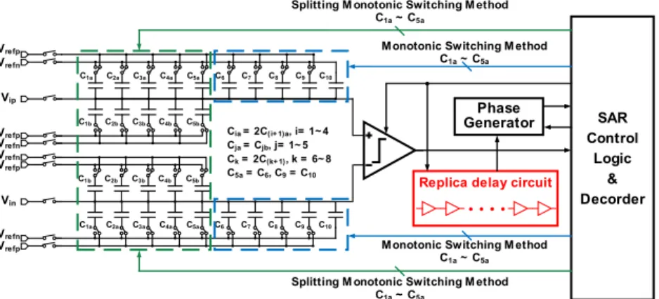
(23) A Low Energy Consumption 10-Bit 100kS/s SAR ADC with Timing Control Adaptive Window Chih-Yuan Kung+, Chun-Po Huang, Chia-Chuan Li, and Soon-Jyh Chang++ Department of Electrical Engineering, National Cheng Kung University, Tainan, 70101, Taiwan Email+: [email protected] and Email++: [email protected] Abstract— This paper presents a 0.35 V 100 kS/s 10-bit successive approximation register (SAR) ADC with adaptive window (AW) in 90 nm CMOS. The SAR ADC uses the transient information of the latch comparator to create redundancy ranges. Furthermore, the proposed technique also uses the transient information to produce AW for each bit which can significantly reduce the power consumption of the comparator, the DAC settling time and also digital control logic. Last but not least, the timing control window can also avoid ADC from encountering meta-stability. The measurement result achieves an SNDR of 57.18 dB, an ENOB of 9.2 bits, a power consumption of 74 nW, and a resulting FoM of 1.25 fJ/conv.-step.. [1]. If the comparator input is among the window, the bit-cycle will be skipped and jump to the corresponding cycle. Nevertheless, the window size in the previous cycles will be restricted by the smallest window. The other kind of window function equipped different window size in each cycle. The largest window size of each cycle can be half of the current cycle’s full swing [2][3][4][5]. In this situation, the window size can be maximized in every cycle. However, the cycles cannot be skipped over owing to the former window size is larger than the current one. The two window function mentioned above can both decrease power consumption and tolerant incomplete settling errors. Nonetheless, they both still have their limit in large window size and skipping cycles.. Keywords—SAR ADC, low-power SAR ADC, timing window, adaptive window, low-vdd,. In this paper, we propose a timing control scheme which combines the benefits of the two window function mentioned above. This proposed technique can save the energy not only from DAC but also digital and other analog circuits by skipping cycles. The details are discussed in Section II, and the simulation results are shown in Section III. Finally, conclusions are drawn in Section IV.. I.. INTRODUCTION. Recently, as the evolution of process technology moves on, lots of complicated circuits are incorporated into portable electronic device. Also, Internet-of-everything (IoE) applications are going to be the trends of future life. As a result, the low-voltage and the low-power issues are worth to deep considering. Successive-approximation register (SAR) analog-to-digital converters (ADCs) are known for their excellent power efficiency and speed improvement in the advanced process technologies. Hence, the SAR ADC is a widely adopted choice for use in the energy-limited systems. For sensors in biomedical circuits, all the data are indispensable because we cannot take the risk of our bodies. It turns out that the circuits have to be robust. When designing reliable ADCs, meta-stability is the one major restriction we have to face with. Meta-stability occurs when the differential inputs are too small, and it will take a long time for the comparator to output the result. This may decrease the ADC speed and even lead to the system break down. By using adaptive window, systems can avoid ADC from encountering meta-stability. In this paper, a new type of window structure of SAR ADCs is proposed which can reduce the power consumption of DACs, the comparator and digital circuits. Also, it enhances the linearity of SAR ADC. Nonetheless, the timing windows create the error tolerance for the DAC settling error and the comparator dynamic offset. For the window functions in SAR ADCs, they can be roughly classified into two categories. The first kind window remains constant-size window through all the skilled cycles. II.. PROPOSED TECHNIQUES. A. Proposed Architecture Figure 1 shows the architecture of the proposed SAR ADC. It consists of a differential S/H circuit, a differential binary-weight DAC, a comparator, a SAR logic control and replica delay circuit for adaptive window (AW) skill. To maintain the common-mode voltage Vcm of comparator’s differential input from encountering dynamic offset, the split monotonic switching skill is implemented on the most significant bit (MSB) to MSB − 4 capacitors and the capacitors are split into half of the original size. Besides, the linearity of the sample and hold circuit in a low supply voltage system should also be concerned. We apply double boost strapped switch skill which creates a constant voltage difference “2VDD” between the gate and source termination and lower down the on resistance of the switches. The replica delay circuit duplicates the operation time of the dynamic comparator. To record the operation time, both the trigger signals of dynamic comparator and replica delay circuit are Clkc. More details will be discussed in the subsection II.B. The proposed architecture includes redundant ranges which can tolerate the DAC settling errors and comparison errors in the conversions, however we do not need extra capacitors or cycles..
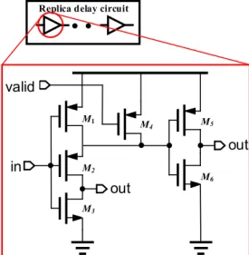
(24) Splitting M onotonic Switching M ethod C1a ~ C5a M onotonic Switching M ethod C1a ~ C5a. Vrefp Vrefn C1a. C2a. C3a. C4a. C5a. C1b. C2b. C3b. C4b. C5b. C1b. C2b. C3b. C4b. C5b. C1a. C2a. C3a. C4a. C5a. C6. C7. C8. C9. C10. Vip Vrefp Vrefn Vrefn Vrefp. Cia = 2C(i+ 1)a, i= 1~ 4 Cja = Cjb, j= 1~ 5 Ck = 2C(k+ 1) , k = 6~ 8 C5a = C6, C9 = C10. Phase Generator. Replica delay circuit. Vin Vrefn Vrefp. C6. C7. C8. C9. SAR Control Logic & Decorder. C10. M onotonic Switching M ethod C1a ~ C5a Splitting M onotonic Switching M ethod C1a ~ C5a. Fig. 1. The architecture of the proposed 10-bit SAR ADC.. B. Adaptive Window While SAR operation performs a low energy, there are some parts to be improved. The comparator and DAC in low voltage supply are relative power consuming part of an SAR ADC. One can adopt low power switching method [7][8] or window function [1][2][3][4] to decrease power consumption. In order to fully utilize the benefit of the voltage window function, we need another source domain information to distinguish the input range. The information may be roughly but much faster. By sensing the comparison time, we can obtain the difference of the input signal. The larger input signal is; the comparator works faster. Consider comparator as a single-pole response [3], the comparator function can be expressed as follows: (. ). = ( )e (1) where A is the gain of comparator, is the comparator input is the available comparator output for backend voltage, digital circuits and is the time constant. This operation time varies linearly as the full-scale voltage scaled down. The comparison time of each stage in full-scale can be modeled as follow: ( ) (. −. (. ) = (. ( ) ). (2). ). where is a constant term. Figure 2 shows the variation time of a dynamic comparator.. As we know from above that the voltage domain information can be transferred into time domain and it varies in grade. It helps ADC predict the input range while comparing which can be applied to window function. Figure 3 shows the circuit diagram of proposed adaptive window skill. Clkc is the active signal of dynamic comparator and also replica delay circuit. While the comparator is operating, replica delay circuit records the time concurrently. The delay circuit creates five timing scales which correspond to voltage windows of the first five stages. Each window scale is between half to quarter full-scale of the current stage. If the voltage comparator does not output the result before the replica delay circuit reaches the first window, the window function will be triggered. Once the first window is triggered, the replica delay circuit continues counting for the second window and so on. Until comparator outputs the result, the replica delay circuit stops counting. Next, digital circuit and replica delay circuit give phase generator information to decide which stage of the capacitor should be switched. If the voltage comparator outputs the result before the replica delay circuit, the SAR ADC works as a conventional one. Figure 4 shows the timing diagram of the conventional ternary SAR ADC and proposed adaptive window SAR ADC with the same inputs. When the voltage comparator is activated, both the replica delay circuit starts to count for the first timing window. If the voltage comparator not outputs the result before the delay circuit stops, the window function will be triggered. However, the ternary SAR ADC’s comparator start to reset for the next comparison and so does the replica delay circuit. While adaptive window SAR ADC’s clk1. Phase gen.. Bitp1 Bitn1. clk2. clk9. Bitp2 Bitn2. Bitp9 Bitn9. clks valid. tri. tri. tri. EN. EN. EN. Oncetriggered latch. clkc. Replica delay circuit Fig. 2. Comparator operation time versus the full-scale input signal of each stage.. Fig. 3. Comparator operation time versus the full-scale input signal of each stage..
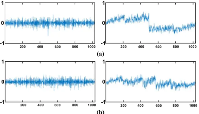
(25) V-comp. Reset. V-comp TDC. TDC. Reset TDC. V-comp TDC. TDC. Reset. TDC. T DAC. (a) Reset. V-comp TDC. TDC. V-comp TDC. T. V-comp. V-comp. Voltage comparator active. TDC. Replica delay circuit. DAC. DAC settle Output a bit. DAC. (b) Fig. 4. The timing diagram of (a) ternary SAR and (b) adaptive window SAR with same input.. comparator keeps operating and it takes the advantage of the delay time from former window. As the window gets smaller, the corresponding delay time grows longer. Adaptive window reuses the delay which was created for previous window which not only saves time from reset and repeatable delay, but also decreases the power of both replica delay circuit and dynamic comparator. C. Control Circuit To perform the adaptive window skill, the replica delay circuit has been adopted in proposed SAR ADC. However, the implementation of the method requires additional control circuits which receive the signals from comparator and replica delay circuits. For a conventional asynchronous SAR ADC, one needs to create Clki signal to indicate which stage is processing in order to switch corresponding capacitors. Usually we apply shift register [7] or compact [9] to create Clki. The proposed adaptive window skill only needs to add once-triggered latches to conventional compact to realize control function. Figure 3 also shows the modified compact circuit for adaptive window. Clki comes from two sources. The first one is from differential capacitor. If either one of the capacitors of current stage is switched, the stage is regarded. as finished. However, while the window function is triggered, both the capacitors remain non-switch. At this situation, the Clki signal comes from replica delay circuit. To keep the Clki high through all conversion till sample signal reset, we apply once-triggered latch to maintain the result of the replica delay circuit. Figure 5 shows the circuit of a unit buffer of replica delay circuit. In order to lower down the power consumption, one needs to increase the delay time with less loading. The buffer is designed with skew to get more delay in main path and fast settle in reset phase. Moreover, M2 and M3 are separated and cascaded. First, intentionally induce body effect to M2, which increase the threshold voltage with source voltage. Second, the effect of drain-induced barrier lowering (DIBL) which also increases the threshold voltage and increases delay with less power consumption. III.. The proposed SAR ADC was designed in TSMC TN90GUTM 90nm CMOS process. The test chip area is 0.8836 mm2, and core circuits occupy 0.04 mm2. The chip layout is shown in Figure 6. The post-simulation result on TABLE I. shows the variation of first and second window between different corner.. Replica delay circuit. valid M1. M4. M5. out in. M2. out. SIMULATION RESULTS. M6. M3. Fig. 5. The circuit diagram of unit buffer of replica delay circuit.. Fig. 6. Die photo..
(26) 1. 1. 0. 0. -1. 200. 400. 800. 600. -1. 1000. TABLE II.. 200. 400. 600. 800. PERFORMANCE SUMMARY AND COMPARISON WITH THE STATEOF-THE-ART ADCS. ISSCC’15 [10]. VLSI’15 [11]. VLSI’12 [6]. This Work. Technology(nm). 65. 180. 90. 90. Supply Voltage(V). 0.6. 0.6. 0.35. 0.35. 1000. (a) 1. 1. Sampling Rate(KS/s). 100. 100. 100. 100. 0. 0. Resolution(bit). 10. 8. 10. 10. Nyquist SNDR(dB). 57.3. 46.9. 56.3. 57.18. Power(nW). 88. 120. 170. 74. FoM(fJ/step). 1.5. 6.6. 3.2. 1.25. -1. 200. 400. 800. 600. -1. 1000. 200. 400. 600. 800. 1000. (b). Fig. 7. The measured DNL and INL (a) without and (b) with adaptive window.. The two extreme cases of first window vary from 0.391 to 0.483 Vref, and second window vary from 0.147 to 0.240 Vref respectively. To prevent DAC array from non-convergence, the window size should not be larger than half of the stage full-scale. Therefore, the redundancy range variations in both cycles do not distort the operations. The measured differential non-linearity (DNL) and integral non-linearity (INL) is plotted in Figure 7 where peak values are -0.45/0.37 and -0.42/0.37 LSB, respectively. The measured SNDR achieves 57.18dB (ENOB is 9.21 bits) at 100KS/s with 50KHz input. The circuit operates at 0.35 V supply voltage and the total power consumption with and without adaptive window is 74.04 nW and 85.33 nW respectively. As a consequence, the skill reduces about 13% power consumption of whole SAR ADC. The figure-of-merit (FoM) is 1.25 fJ/Conv.-step. Table II. shows the similar-resolution comparison result among this work and other state-of-the-art SAR ADCs. IV.. CONCLUSION. This paper presents a circuit technique which combines the advantages of static window and dynamic window. Adaptive window optimizes the window size to give SAR ADC not only more redundant ranges but also decrease power consumption. Furthermore, the window function omits unnecessary switching, which diminishes the impacts of capacitor mismatch. The simulation results demonstrate the effectiveness in enhancing the performance and robustness for the SAR ADCs.. TABLE I.. CORNER VARIATION OF REPLICA DELAY CIRCUIT. Voltage variation. TT. FF. FS. SF. SS. Window #1. 0.450 Vref. 0.444 Vref. 0.391 Vref. 0.457 Vref. 0.483 Vref. Window #2. 0.219 Vref. 0.147 Vref. 0.205 Vref. 0.126 Vref. 0.240 Vref. ACKNOWLEDGMENT This work was supported by the grant from Ministry of Science and Technology in Taiwan under Grant MOST (1052221-E-006-240-MY3). REFERENCES [1]. G. Y. Huang, S. J. Chang, C. C. Liu and Y. Z. Lin, “A 1-µW 10-bit 200-kS/s SAR ADC With a Bypass Window for Biomedical Applications,” in IEEE Journal of Solid-State Circuits, vol. 47, no. 11, pp. 2783–2795, Nov. 2012. [2] C. C. Liu, S. J. Chang, G. Y. Huang, Y. Z. Lin and C. M. Huang, “A 1V 11fJ/conversion-step 10bit 10MS/s asynchronous SAR ADC in 0.18µm CMOS,” in IEEE Symp. VLSI Circuits Dig. Tech. Papers, 2010, pp.241–242. [3] J. Guerber, H. Venkatram, M. Gande, A. Waters and U. K. Moon, “A 10-b Ternary SAR ADC With Quantization Time Information Utilization,” in IEEE Journal of Solid-State Circuits, vol. 47, no. 11, pp. 2604–2613, Nov. 2012.. [4] Y. H. Chung, M. H. Wu and H. S. Li, “A 24μW 12b 1MS/s 68.3dB SNDR SAR ADC with two-step decision DAC switching,” in IEEE Custom Integrated Circuits Conference, 2013, pp. 1–4. [5] Y. H. Chung, C. H. Tsai and H. C. Yeh, “A 5-b 1-GS/s 2.7-mW binarysearch ADC in 90nm digital CMOS,” in IEEE International Systemon-Chip Conference, 2015, pp. 25–29. [6] Y.-H. Chung, “The Swapping Binary-Window DAC Switching Technique for SAR ADCs,” in Proc. IEEE ISCAS, 2013, pp. 2231– 2234. [7] Chun-Cheng Liu, Soon-Jyh Chang, Guan-Ying Huang, and Ying-Zu Lin, “A 10-bit 50-MS/s SAR ADC with a Monotonic Capacitor Switching Procedure,” in IEEE Journal of Solid-State Circuits, vol.45, no.4, pp.731–740, Apr. 2010. [8] V. Hariprasath, J. Guerber, S. H. Lee and U. K. Moon, “Merged capacitor switching based SAR ADC with highest switching energyefficiency,” in IEEE Electronics Letters, vol. 46, no. 9, pp. 620–621, April 29 2010. [9] Che-Hsun Kuo and Soon-Jyh Chang “A 10–bit 120–MS/s SAR ADC with compact architecture and noise suppression technique, ” Department of Electrical Engineering, National Cheng Kung University, Tainan, Taiwan,Thesis for Master of Science, July, 2014 [10] P. Harpe, H. Gao, R. van Dommele, E. Cantatore and A. van Roermund, “21.2 A 3nW signal-acquisition IC integrating an amplifier with 2.1 NEF and a 1.5fJ/conv-step ADC,” in IEEE International Solid-State Circuits Conference Dig. Tech. Papers, 2015, pp. 1–3. [11] S. Jeong et al., "A 120nW 8b sub-ranging SAR ADC with signaldependent charge recycling for biomedical applications,” in IEEE Symp. VLSI Circuits Dig. Tech. Papers, 2015, pp. C60–C61. [12] H. Y. Tai, H. W. Chen and H. S. Chen, “A 3.2fJ/c.-s. 0.35V 10b 100KS/s SAR ADC in 90nm CMOS,” in IEEE Symp. VLSI Circuits Dig. Tech. Papers, 2012, pp. 92-93..
(27) 106年度專題研究計畫成果彙整表 計畫主持人:張順志. 計畫編號:106-2221-E-006-238-MY3. 計畫名稱:應用於物聯網系統之感測器與類比至數位轉換器之研製 成果項目. 學術性論文. 量化. 期刊論文. 0. 研討會論文. 0. 專書. 0 本. 專書論文. 0 章. 技術報告. 0 篇. 其他. 0 篇. 專利權 國 內. 發明專利. 申請中. 0. 已獲得. 0. 新型/設計專利. 篇. 0. 商標權 智慧財產權 營業秘密 及成果 積體電路電路布局權. 0. 著作權. 0. 品種權. 0. 其他. 0. 件數. 0 件. 收入. 0 千元. 期刊論文. 0. 研討會論文. 0. 專書. 0 本. 專書論文. 0 章. 技術報告. 0 篇. 其他. 0 篇. 技術移轉. 學術性論文. 國 外. 質化 (說明:各成果項目請附佐證資料或細 單位 項說明,如期刊名稱、年份、卷期、起 訖頁數、證號...等) . 專利權. 發明專利. 0 件 0. 申請中. 0. 已獲得. 0. 新型/設計專利. 篇. 0. 商標權 智慧財產權 營業秘密 及成果 積體電路電路布局權. 0. 著作權. 0. 品種權. 0. 其他. 0. 0 件 0.
(28) 技術移轉. 本國籍 參 與 計 畫 人 力 非本國籍. 件數. 0 件. 收入. 0 千元. 大專生. 0. 碩士生. 0. 博士生. 0. 博士後研究員. 0. 專任助理. 0. 大專生. 0. 碩士生. 6. 博士生. 0. 博士後研究員. 0. 專任助理. 0. 其他成果 (無法以量化表達之成果如辦理學術活動 、獲得獎項、重要國際合作、研究成果國 際影響力及其他協助產業技術發展之具體 效益事項等,請以文字敘述填列。) . 人次 提供6人年碩士班學生獎助金。. 1. 2017晶片製作成果發表會優良晶片遴選,優等設計獎 。 2. 協助聯詠半導體公司開發low BER SAR ADC。(產學合 作) 3. 協助奇景公司開發High-linearity SAR ADC。(產學合 作).
(29) 科技部補助專題研究計畫成果自評表 請就研究內容與原計畫相符程度、達成預期目標情況、研究成果之學術或應用價 值(簡要敘述成果所代表之意義、價值、影響或進一步發展之可能性)、是否適 合在學術期刊發表或申請專利、主要發現(簡要敘述成果是否具有政策應用參考 價值及具影響公共利益之重大發現)或其他有關價值等,作一綜合評估。 1. 請就研究內容與原計畫相符程度、達成預期目標情況作一綜合評估 ■達成目標 □未達成目標(請說明,以100字為限) □實驗失敗 □因故實驗中斷 □其他原因 說明: 2. 研究成果在學術期刊發表或申請專利等情形(請於其他欄註明專利及技轉之證 號、合約、申請及洽談等詳細資訊) 論文:□已發表 □未發表之文稿 ■撰寫中 □無 專利:□已獲得 ■申請中 □無 技轉:□已技轉 ■洽談中 □無 其他:(以200字為限) 與奇景光電公司、聯詠半導體公司產學合作SAR ADC IC設計相關議題。 3. 請依學術成就、技術創新、社會影響等方面,評估研究成果之學術或應用價值 (簡要敘述成果所代表之意義、價值、影響或進一步發展之可能性,以500字 為限) 類比至數位轉換器是電子電路系統的關鍵元件,本計畫的研發成果旨在提高類 比至數位轉換器的穩定度、降低轉換耗能,並使其易於與感測器整合,所開發 的技術一方面可協助業界開發前瞻的物聯網電子產品、促進經濟發展外,亦有 助於朝向節能減碳的永續環境發展。 計畫所開發的架構與電路技術,以及所研製的高效能類比至數位轉換晶片,具 有相當程度的創新性與進步性,有一定的學術價值。於SAR ADC IC設計議題 ,計畫成果對台灣在世界上的學術成就應有一定程度的貢獻。 4. 主要發現 本研究具有政策應用參考價值:■否 □是,建議提供機關 (勾選「是」者,請列舉建議可提供施政參考之業務主管機關) 本研究具影響公共利益之重大發現:□否 □是 說明:(以150字為限).
(30)
數據
相關文件
HP(COMPAQ)伺服器為主,作業系統多為 Windows,僅有少數為 Linux,多 數主機均已置於 VMware 虛擬化平台上,應用軟體架構大部分為 Web-Base(網 路架構示意圖如
國立政治大學應用數學系 林景隆 教授 國立成功大學數學系 許元春召集人.
、機構應於受理之日起三十日內通知其復職,留職停薪人員應於服 務之學校、機構通知之日起,三十日內復職報到;其未申請提前復
回答: 1、臨櫃講習時雇主或代講習人員,需至公立就業服務機構參加。參 加講習人員可於聘前講習系統上先行預約,於預約時間至公立就
數位計算機可用作回授控制系統中的補償器或控制
Complex Instruction Set Computers (CISC). complicated
為此,國立中正大學防制藥物濫用教育中心與台灣藥物濫用防治研究學會,在教育部學生事 務及特殊教育司之支持下,將於 2019 年 10 月
之意,此指依照命令動作的意義。所謂伺服 系統,就是依照指示命令動作所構成的控制
