Investigation of void nucleation and propagation during electromigration of flip-chip
solder joints using x-ray microscopy
S. H. Chiu and Chih Chen
Citation: Applied Physics Letters 89, 262106 (2006); doi: 10.1063/1.2425040
View online: http://dx.doi.org/10.1063/1.2425040
View Table of Contents: http://scitation.aip.org/content/aip/journal/apl/89/26?ver=pdfcov Published by the AIP Publishing
Articles you may be interested in
Effect of void propagation on bump resistance due to electromigration in flip-chip solder joints using Kelvin structure
Appl. Phys. Lett. 91, 132113 (2007); 10.1063/1.2790376
Effect of Al-trace degradation on Joule heating during electromigration in flip-chip solder joints Appl. Phys. Lett. 90, 082103 (2007); 10.1063/1.2644061
Study of void formation due to electromigration in flip-chip solder joints using Kelvin bump probes Appl. Phys. Lett. 89, 032103 (2006); 10.1063/1.2226989
Infrared microscopy of hot spots induced by Joule heating in flip-chip SnAg solder joints under accelerated electromigration
Appl. Phys. Lett. 88, 022110 (2006); 10.1063/1.2151255
Effect of current crowding and Joule heating on electromigration-induced failure in flip chip composite solder joints tested at room temperature
J. Appl. Phys. 98, 013715 (2005); 10.1063/1.1949719
This article is copyrighted as indicated in the article. Reuse of AIP content is subject to the terms at: http://scitation.aip.org/termsconditions. Downloaded to IP: 140.113.38.11 On: Thu, 01 May 2014 01:39:52
Investigation of void nucleation and propagation during electromigration
of flip-chip solder joints using x-ray microscopy
S. H. Chiu and Chih Chena兲
Department of Material Science and Engineering, National Chiao Tung University, Hsin-chu 30050, Taiwan, Republic of China
共Received 21 September 2006; accepted 26 November 2006; published online 27 December 2006兲 X-ray microscopy was employed to investigate void nucleation and propagation during electromigration in solder joints. The shape of the voids at various stages can be clearly observed. The voids became irregular when they propagated to deplete the contact opening. Growth velocity at the early stage was found to be 1.3m / h under 6.5⫻103A / cm2at 150 ° C, and it decreased to 0.3m / h at later stages. Formation of intermetallic compound共IMC兲 and compositional changes at the interface of solder/IMC on the chip side were attributed to the retarded growth rate at later stages. © 2006 American Institute of Physics.关DOI:10.1063/1.2425040兴
To meet the demand for higher performance in portable microelectronic device applications, flip-chip technology has been adopted for high-density packaging due to its excellent electrical characteristics and superior heat dissipation capa-bility. With the increase in the required performance in mi-croelectronic devices, the current that each bump has to carry is also on the increase.1 The corresponding current density may reach 1⫻104A / cm2 in the near future. Under such a high current density at the solder bump, electromigration in-evitably becomes a critical reliability issue.2,3
During electromigration, voids nucleate in the solder bump near the point of entry of electron flow, where serious current crowding and flux divergence occur.4–7With the in-crease in stressing time, void propagates towards the rest of the under bump metallization 共UBM兲 opening, resulting in open failure of the joints. In previous studies, void formation and propagation were observed by cross-sectional scanning electron microscope共SEM兲. Therefore, only the length and the depth of the void at those specific cross sections can be observed. However, the location where voids nucleate, the shape of voids, as well as how voids propagate in the UBM opening remain unclear. In addition, the propagation veloci-ties of voids at different stages have not been measured.
X-ray microscopy has been employed to study formation of voids in Cu interconnects during electromigration.8 Since the size of voids formed in Cu interconnects is in submicron range, synchrotron radiation x ray is needed. For flip-chip solder joints, the voids are of a much larger dimension, typi-cally ranging from few microns to tens of microns. Thus, a laboratory-based x-ray microscope appears to be sufficient for the investigation of void nucleation and propagation in solder joints during electromigration. Nevertheless, it has not been applied to solder joints.
In this letter, void formation during electromigration was monitored by an x-ray microscope. The area of the voids was measured from the x-ray images, with which the velocity of void propagation was calculated. This approach provides a deeper understanding on the behavior of void nucleation and propagation during electromigration in solder joints.
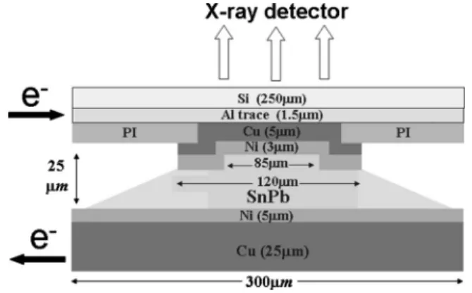
Figure 1共a兲 shows the cross-sectional schematic for the solder joint used in this study. The Al trace was 1.5m thick and 100m wide, while Cu lines on the substrate were 25m thick and 100m wide. The UBM consists of 0.1m Ti, 5m Cu, and 3m Ni layers. The diameters of the UBM and the passivation openings were 120 and 85m, respectively. Electroplated SnPb solder bumps were mounted on an FR4 substrate to form flip-chip joints. Non-solder-mask-defined process was used in this structure. The dimen-sion of the Cu pad opening was 300m in diameter. Owing to the large opening in the substrate side, the bump height was as small as 25m. With the low bump height, the voids in the solder bump would be much clearly seen in an x-ray microscope. The solder joints were stressed by 0.8 A at 150 ° C for a desired time. The direction of the electron flow was indicated by the arrows in the figure. Then they were examined by a Dage XL-6500 x-ray microscope with the Si side facing the x-ray detector, whose spatial resolution is 2m. The corresponding current density was 6.5 ⫻103A / cm2. The operation voltage was set at 95 kV in this study. Since voids form in the bump with electron flow from the chip side to the substrate side, only the bumps with this stressing direction were examined. SEM was also employed to examine the voids in the cross section of the solder bumps.
The shape of the voids induced by electromigration can be clearly observed using x-ray microscope. Figure 2共a兲
shows the x-ray image of the solder joints before current
a兲Author to whom correspondence should be addressed; electronic mail:
[email protected] FIG. 1. Cross-sectional schematic diagram of the samples used in this study.
APPLIED PHYSICS LETTERS 89, 262106共2006兲
0003-6951/2006/89共26兲/262106/3/$23.00 89, 262106-1 © 2006 American Institute of Physics
This article is copyrighted as indicated in the article. Reuse of AIP content is subject to the terms at: http://scitation.aip.org/termsconditions. Downloaded to IP: 140.113.38.11 On: Thu, 01 May 2014 01:39:52
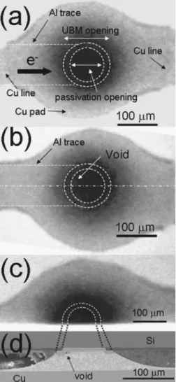
stressing. Since the Al trace is quite thin and the density of Al is low, it is not visible in the x-ray image. The position of the Al trace was denoted by the two dashed lines in Fig.2共a兲. Since the Cu line in the substrate was as thick as 25m, it was visible in the x-ray image. To facilitate the observation of void formation, the passivation and UBM openings were marked on the image by two dotted white circles. The center region shows a darker image due to the Cu/ Ni UBM and thicker solder in this region. After current stressing at 0.8 A at 150 ° C for 29.8 h, the same sample was examined again by x-ray microscope. A small brighter region was observed near the left corner of the UBM opening, where the electrons crowded into the solder bump. Furthermore, the voids ex-tended backwards to the UBM opening because the UBM layer may serve as a conducting path for electrons.6,9 The shape of void appears to be irregular. This specimen was labeled as sample A in this letter. To verify if voids were formed in this region, the sample was ground and polished laterally to approximate the center of the bump, and it was inspected again by x-ray microscope, as shown in Fig.2共c兲. The location of the cross section is also indicated by the middle dashed line in Fig. 2共b兲. Then it was examined by SEM to reveal the location of voids, as shown in Fig.2共d兲. As can be seen, the void position matched that obtained by
x-ray microscope. Therefore, x-ray microscopy can be em-ployed to observe void formation.
The growth velocity of the voids can be calculated from the x-ray images. To obtain the growth velocity at different stages, four more samples were stressed for different lengths of time and then examined by x-ray microscopy and SEM. They were labeled as samples B–E in this letter. Figures
3共a兲–3共d兲show the x-ray images of the four samples stressed at 0.8 A at 150 ° C for 37.8, 110.2, 177.8, and 384.0 h, re-spectively. The corresponding SEM images were shown in Figs.4共a兲–4共d兲. Larger voids were formed with the increase in stressing time, and the voids propagated from the left-hand side to the right-left-hand side. In addition, the voids be-came irregular as they propagated, as shown in Figs.
3共b兲–3共d兲. The heights of the voids were larger. Thus, the void contrast was better for the x-ray image. SEM image shows that thicker intermetallic compounds 共IMCs兲 of Ni3Sn4 were formed between the Ni UBM and solder, as indicated by the arrows in the SEM images in Figs.4共c兲and
4共d兲. Both x-ray and SEM images indicate that the voids in samples D and E became discontinuous. Because the IMC has better electromigration resistance than the solder, void propagation would be hindered by the IMC grains. To calcu-late the growth velocity of the voids, the area of voids was calculated from the x-ray images by a computer software. Figure5共a兲shows the area of voids as a function of stressing
FIG. 2.共a兲 Plan-view x-ray image of the joint before current stressing. The UBM and passivation openings were labeled by the dotted white circles.共b兲 X-ray image of the same joint after current stressing. The void was enclosed by the white line.共c兲 X-ray image of the same joint after being polished laterally to middle of the joint.共d兲 Cross-sectional SEM image of the joint in 共c兲. A void formed near the entrance of the Al trace.
FIG. 3. Plan-view x-ray images of the joint after stressing for共a兲 37.8 h, 共b兲 110.2 h,共c兲 177.8 h, and 共d兲 384.0 h. The position of the Al trace was labeled by the dotted lines in the figures.
FIG. 4. Corresponding cross-sectional SEM images of the joint in Figs.
3共a兲–3共d兲.
262106-2 S. H. Chiu and C. Chen Appl. Phys. Lett. 89, 262106共2006兲
This article is copyrighted as indicated in the article. Reuse of AIP content is subject to the terms at: http://scitation.aip.org/termsconditions. Downloaded to IP: 140.113.38.11 On: Thu, 01 May 2014 01:39:52
time for the above five samples, and it increased with the increase in stressing time. The slope between the first two points was higher. The reason will be discussed later. To calculate the average growth velocity, the maximum length along the propagation direction, which is the positive X axis, was adopted as the propagation length. Then the growth ve-locity was calculated on the basis of the void propagation length and the stressing time. Figure5共b兲illustrates the av-erage growth velocity for the five samples. It is found that the average growth velocity was 1.3m / h for sample A. It increased to 1.8m / h for sample B, and it decreased to 0.6m / h for sample C, 0.5m / h for sample D, and 0.3m / h for sample E. In addition, the depletion percent-ages of UBM opening were 17.8%, 23.1%, 55.6%, 78.0%, and 94.0% for the five samples, as labeled in Fig.5共b兲.
The incubation time for void formation may be respon-sible for the low growth velocity for sample A in the initial stage. Under the condition of current stressing, the incuba-tion time was about 20 h for the solder joints used in this study. Only a small void was formed in sample A. Therefore, the velocity was low for sample A. Once the voids were formed, they propagated more quickly, as shown in sample B. The measured velocity was 1.4 times faster than that of sample A. However, the velocity decreased for samples C, D–E. The above findings are quite different from those for Al and Cu interconnects. At later stages of electromigration in Al and Cu interconnects, the growth rate of voids became higher due to the much higher current density around the
voids. In addition, for solder joints with thin-film UBM, the voids also grew faster at later stages.10 It is speculated that IMC formation and compositional changes may be respon-sible for the low velocities of our samples at later stages. For the former, Ni3Sn4may inhibit void propagation, as shown in Figs.4共c兲and4共d兲. For the latter, solder composition at the IMC/solder interface changes to pure Sn at later stages, as also shown in Figs.4共c兲and4共d兲. Since pure Sn has higher electromigration resistance than eutectic solder,11void propa-gation would be slowed down at later stages. In addition, it is reported that the current crowding effect is relieved as the voids propagate before depleting half of the UBM opening,9 since the current is spread out more uniformly in the Al pad directly above the voids. For sample E, current crowding effect became worse, yet the growth rate decreased to 0.3m / h, indicating that IMC formation and compositional change dominated the growth velocity of voids.
Compared with the growth velocity reported by Zhang et al., the value obtained in this study was slightly smaller. Their testing conditions were 3.67⫻103A / cm2 at 146 ° C on 95.5Sn− 4.0Ag− 0.5Cu solder joints with Al/ Ni共V兲/Cu thin-film UBM. The growth velocity of voids they obtained was about 4.4m / h. In contrast, our testing conditions were 6.5⫻103A / cm2 at 150 ° C, which are more severe than theirs. It is speculated that the thick UBM layer may slow down void propagation. The UBM used in this study was 5m Cu/ 3m Ni. It is reported that this thick UBM layer can relieve the current crowding effect by a factor of 3.3 times, compared with Al/ Ni共V兲/Cu thin-film UBM. There-fore, the growth velocity of voids was slower for solder joints with a thick-film UBM.
In summary, x-ray microscopy can detect void nucle-ation and propagnucle-ation in flip-chip solder joints. The voids nucleated in the vicinity of the entrance point of Al trace, and their shape was quite irregular. The growth velocity was measured to be around 0.3– 1.8m / h at various stages un-der 6.5⫻103A / cm2 at 150 ° C for SnPb solder joints with thick-film Cu/ Ni UBM.
The authors would like to thank National Science Coun-cil of Taiwan of R.O.C. for the financial support through Grant No. NSC 95-2218-E-009-022.
1K. N. Tu, J. Appl. Phys. 94, 5451共2003兲.
2International Technology Roadmap for Semiconductors, Assembly and Packaging Section, Semiconductor Industry Association, San Jose, CA, 2003, pp. 4–9.
3C. Y. Liu, Chih Chen, C. N. Liao, and K. N. Tu, Appl. Phys. Lett. 75, 58 共1999兲.
4Everett C. C. Yeh, W. J. Choi, and K. N. Tu, Appl. Phys. Lett. 80, 4 共2002兲.
5J. W. Nah, K. W. Paik, J. O. Suh, and K. N. Tu, J. Appl. Phys. 94, 7560 共2003兲.
6L. Zhang, S. Ou, J. Huang, K. N. Tu, St. Gee, and L. Nguyen, Appl. Phys. Lett. 88, 012106共2006兲.
7Y. W. Chang, S. W. Liang, and Chih Chen, Appl. Phys. Lett. 89, 032103 共2006兲.
8G. Schneider, G. Denbeaux, E. H. Anderson, B. Bates, A. Pearson, M. A. Meyer, E. Zschech, D. Hambach, and E. A. Stach, Appl. Phys. Lett. 81, 2535共2002兲.
9S. W. Liang, Y. W. Chang, T. L. Shao, Chih Chen, and K. N. Tu, Appl. Phys. Lett. 89, 022117共2006兲.
10W. J. Choi, E. C. C. Yeh, and K. N. Tu, J. Appl. Phys. 94, 5665共2003兲. 11C. Y. Liu, Chih Chen, and K. N. Tu, J. Appl. Phys. 88, 5703共2000兲. FIG. 5.共a兲 Plot of depletion area as a function of stressing time. 共b兲 Plot of
void growth velocity against stressing time for the five samples. The deple-tion percentage of UBM opening for each sample was also shown in the figure.
262106-3 S. H. Chiu and C. Chen Appl. Phys. Lett. 89, 262106共2006兲
This article is copyrighted as indicated in the article. Reuse of AIP content is subject to the terms at: http://scitation.aip.org/termsconditions. Downloaded to IP: 140.113.38.11 On: Thu, 01 May 2014 01:39:52