Double-transconductance-plateau characteristics in InGaAs Õ GaAs real-space transfer high-electron-mobility transistor
Ching-Sung Lee
a)Department of Electronic Engineering, Feng Chia University, 100 Wenhwa Road Taichung 40724, Taiwan, Republic of China
Wei-Chou Hsu
Institute of Microelectronics, Department of Electrical Engineering, National Cheng Kung University, 1 University Road, Tainan 70101, Taiwan, Republic of China
共Received 3 December 2003; accepted 19 March 2004; published online 20 April 2004兲
Bias-tunable double-transconductance-plateau characteristics due to real-space transfer through the lowering of conduction band offset at high electric fields in a ␦ -doped InGaAs/GaAs high-electron-mobility transistor have been observed. Extrinsic, unpassivated peak performance values, with gate dimensions of 1 ⫻125 m
2, include the transconductance plateaus of 269 and 116 mS/mm at V
DS⫽3 V for V
GS⫽0 V and ⫺1.5 V, respectively, maximum drain current density of 382 mA/mm at VDS⫽5.5 V, unity current gain cutoff frequency of 15.5 GHz, and maximum frequency of oscillation of 23 GHz. The present structure is promising for high-speed analog-to-digital converters or multiple-state quantizer applications. © 2004 American Institute of Physics. 关DOI: 10.1063/1.1738512兴
A real-space transfer 共RST兲1–3mechanism in compound heterostructure field-effect transistors resulting in negative differential resistance phenomenon has been extensively in- vestigated and widely applied to the microwave and high- power optoelectronic integrated circuits.
4,5 The pronounced N-shaped negative differential resistance
6,7 phenomenon is generally due to the modulation of carrier concentration–
velocity product initiated from the intervalley transfer or the tunneling RST
8,9from a higher speed conduction path to a lower-speed channel. The reverse transition to accomplish an increased saturation current density has not yet been ob- served and resolved for circuit applications. In this letter, bias-dependent double-transconductance-plateau characteris- tics due to the current step-up by RST at high electric fields in a ␦ -doped InGaAs/GaAs high-electron-mobility transistor 共HEMT兲 have been achieved. As the channel potential is sufficiently increased by the applied gate and drain bias to initiate the lowering of conduction band offset, the acceler- ated hot electrons at the main channel will surpass and trans- fer to a higher speed path to contribute to an increased par- allel conduction current. Furthermore, a thickness-graded superlattice spacer is employed for improving the hetero- structure interfacial quality. The proposed device structure can be applied to high-speed logic circuits.
10,11A ␦ -doped pseudomorphic InGaAs/GaAs HEMT device structure was prepared by a low-pressure metalorganic chemical vapor deposition system on a 共100兲 semi-insulating GaAs substrate. The device layer structure consisted of a 0.5
m undoped GaAs buffer layer, an 80 Å undoped In
0.24Ga
0.76As conducting channel, an undoped 15 Å GaAs/20 Å In
0.28Ga
0.72As/30 Å GaAs/10 Å In
0.28Ga
0.72As/45 Å GaAs thickness-graded superlattice spacer, an n
⫹␦ -doped GaAs layer with doping concentration of 5 ⫻1012cm
⫺2, and
finally a 200 Å GaAs cap layer. AuGe/Ni alloy was used for the source and drain contacts, onto which Ag was evaporated to prevent agglomeration and to reduce the contact resis- tance. Mesa etching was performed to reduce the gate leak- age current and obtain good pinch-off characteristics before evaporating Au as the Schottky contact gate electrode.
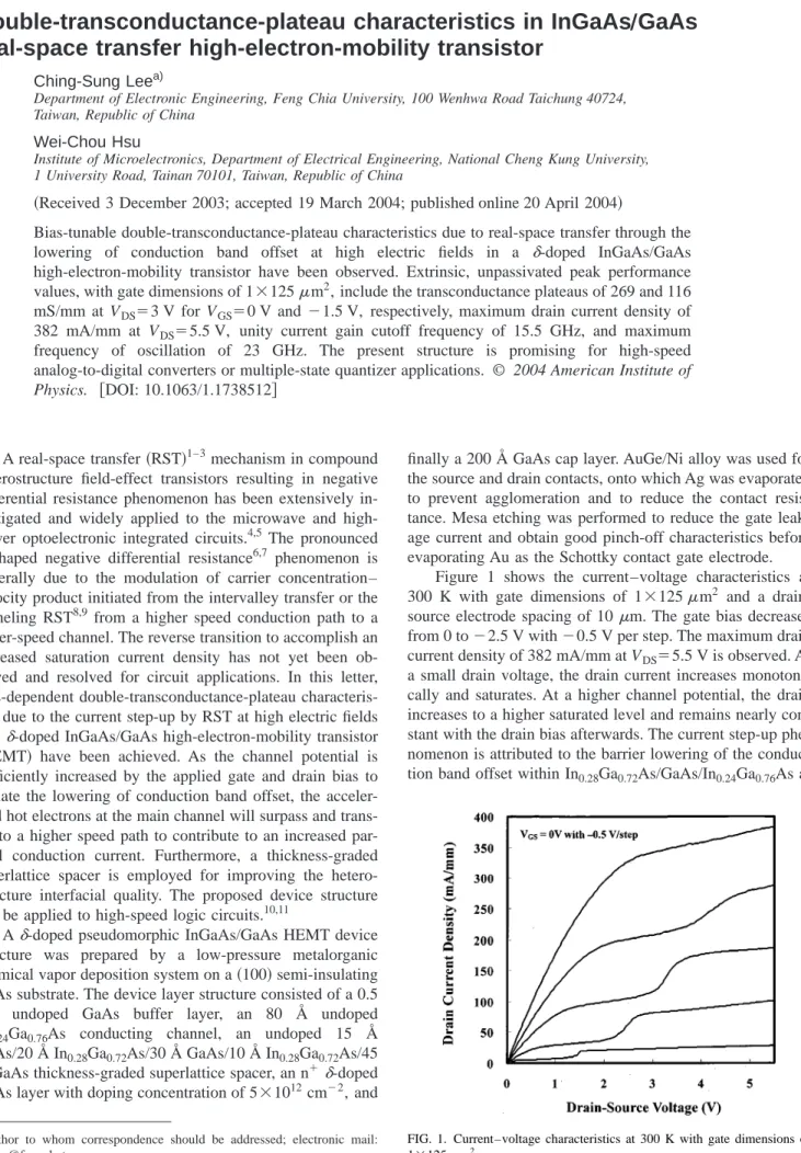
Figure 1 shows the current–voltage characteristics at 300 K with gate dimensions of 1 ⫻125 m
2and a drain/
source electrode spacing of 10 m. The gate bias decreases from 0 to ⫺2.5 V with ⫺0.5 V per step. The maximum drain current density of 382 mA/mm at V
DS⫽5.5 V is observed. At a small drain voltage, the drain current increases monotoni- cally and saturates. At a higher channel potential, the drain increases to a higher saturated level and remains nearly con- stant with the drain bias afterwards. The current step-up phe- nomenon is attributed to the barrier lowering of the conduc- tion band offset within In0.28Ga
0.72As/GaAs/In
0.24Ga
0.76As at
a兲Author to whom correspondence should be addressed; electronic mail:
FIG. 1. Current–voltage characteristics at 300 K with gate dimensions of 1⫻125m2.
APPLIED PHYSICS LETTERS VOLUME 84, NUMBER 18 3 MAY 2004
3618
0003-6951/2004/84(18)/3618/3/$22.00 © 2004 American Institute of Physics
Downloaded 19 Sep 2008 to 140.116.208.41. Redistribution subject to AIP license or copyright; see http://apl.aip.org/apl/copyright.jsp
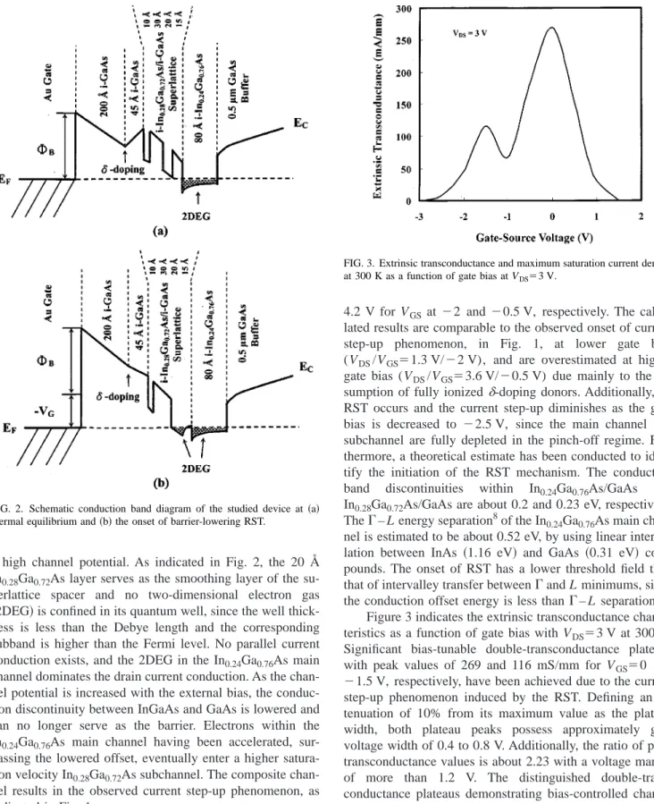
a high channel potential. As indicated in Fig. 2, the 20 Å In
0.28Ga
0.72As layer serves as the smoothing layer of the su- perlattice spacer and no two-dimensional electron gas 共2DEG兲 is confined in its quantum well, since the well thick- ness is less than the Debye length and the corresponding subband is higher than the Fermi level. No parallel current conduction exists, and the 2DEG in the In
0.24Ga
0.76As main channel dominates the drain current conduction. As the chan- nel potential is increased with the external bias, the conduc- tion discontinuity between InGaAs and GaAs is lowered and can no longer serve as the barrier. Electrons within the In
0.24Ga
0.76As main channel having been accelerated, sur- passing the lowered offset, eventually enter a higher satura- tion velocity In
0.28Ga
0.72As subchannel. The composite chan- nel results in the observed current step-up phenomenon, as indicated in Fig. 1.
Calculations
12of the device band diagram under external bias have been conducted to investigate the onset of the RST mechanism. Continuity of electric flux and conduction band offset
13within the heterojunction have been maintained and considered. By assuming the complete ionization case of the
␦ -doping donors, neglecting the unintentional background doping and interfacial states, and applying the gradual- channel approximation along the In
0.24Ga
0.76As channel, the required V
DSbiases to initiate the barrier-lowering of the In
0.28Ga
0.72As/GaAs discontinuity are estimated to be 1.2 and
4.2 V for V
GSat ⫺2 and ⫺0.5 V, respectively. The calcu- lated results are comparable to the observed onset of current step-up phenomenon, in Fig. 1, at lower gate bias (V
DS/V
GS⫽1.3 V/⫺2 V), and are overestimated at higher gate bias (VDS/V
GS⫽3.6 V/⫺0.5 V) due mainly to the as- sumption of fully ionized ␦ -doping donors. Additionally, no RST occurs and the current step-up diminishes as the gate bias is decreased to ⫺2.5 V, since the main channel and subchannel are fully depleted in the pinch-off regime. Fur- thermore, a theoretical estimate has been conducted to iden- tify the initiation of the RST mechanism. The conduction band discontinuities within In0.24Ga
0.76As/GaAs and In
0.28Ga
0.72As/GaAs are about 0.2 and 0.23 eV, respectively.
Ga
0.76As/GaAs and In
0.28Ga
0.72As/GaAs are about 0.2 and 0.23 eV, respectively.
The ⌫ – L energy separation8of the In
0.24Ga
0.76As main chan- nel is estimated to be about 0.52 eV, by using linear interpo- lation between InAs 共1.16 eV兲 and GaAs 共0.31 eV兲 com- pounds. The onset of RST has a lower threshold field than that of intervalley transfer between ⌫ and L minimums, since the conduction offset energy is less than ⌫ – L separation.
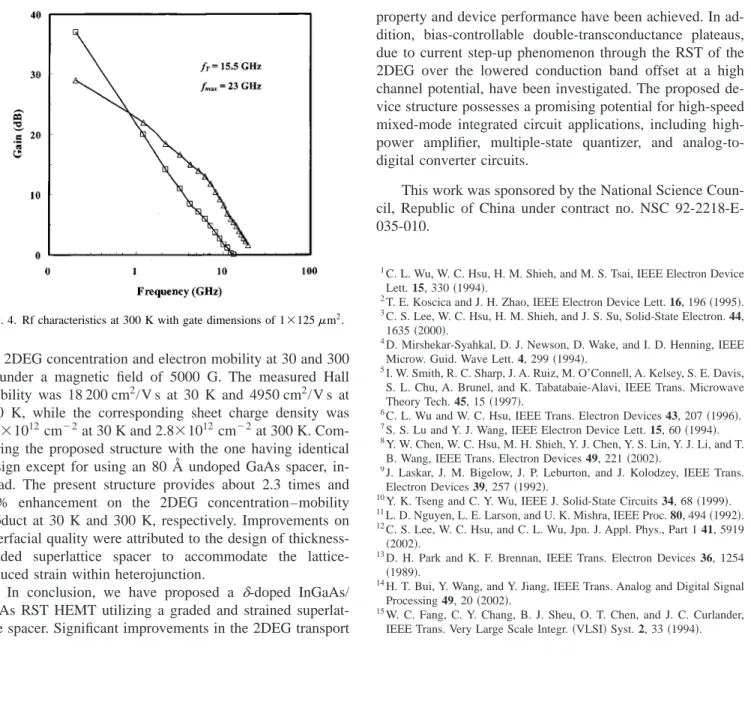
Figure 3 indicates the extrinsic transconductance charac- teristics as a function of gate bias with V
DS⫽3 V at 300 K.
Significant bias-tunable double-transconductance plateaus with peak values of 269 and 116 mS/mm for V
GS⫽0 and
⫺1.5 V, respectively, have been achieved due to the current step-up phenomenon induced by the RST. Defining an at- tenuation of 10% from its maximum value as the plateau width, both plateau peaks possess approximately gate voltage width of 0.4 to 0.8 V. Additionally, the ratio of peak transconductance values is about 2.23 with a voltage margin of more than 1.2 V. The distinguished double-trans- conductance plateaus demonstrating bias-controlled charac- teristics with significant device gains and selectivity can be applied to high-speed multiple-state quantizer and analog-to- digital converter14,15circuit implementations. The character- izations of rf performance for the proposed device at room temperature have been conducted by the HP 8510B network analyzer in conjunction with a Cascade probe station with the frequency range of 0.2 to 20 GHz. As seen in Fig. 4, the unity current gain cutoff frequency f
T and the maximum oscillation frequency f
maxwere determined to be 15.5 and 23 GHz, respectively, with zero gate bias at V
DS⫽3 V.
Hall measurements were also performed to characterize
FIG. 2. Schematic conduction band diagram of the studied device at共a兲 thermal equilibrium and共b兲 the onset of barrier-lowering RST.
FIG. 3. Extrinsic transconductance and maximum saturation current density at 300 K as a function of gate bias at VDS⫽3 V.
3619
Appl. Phys. Lett., Vol. 84, No. 18, 3 May 2004 C. Lee and W. Hsu
Downloaded 19 Sep 2008 to 140.116.208.41. Redistribution subject to AIP license or copyright; see http://apl.aip.org/apl/copyright.jsp
the 2DEG concentration and electron mobility at 30 and 300 K under a magnetic field of 5000 G. The measured Hall mobility was 18 200 cm
2/V s at 30 K and 4950 cm
2/V s at 300 K, while the corresponding sheet charge density was 2.1 ⫻1012cm
⫺2at 30 K and 2.8 ⫻1012cm
⫺2at 300 K. Com- paring the proposed structure with the one having identical design except for using an 80 Å undoped GaAs spacer, in- stead. The present structure provides about 2.3 times and 45% enhancement on the 2DEG concentration–mobility product at 30 K and 300 K, respectively. Improvements on interfacial quality were attributed to the design of thickness- graded superlattice spacer to accommodate the lattice- induced strain within heterojunction.
cm
⫺2at 300 K. Com- paring the proposed structure with the one having identical design except for using an 80 Å undoped GaAs spacer, in- stead. The present structure provides about 2.3 times and 45% enhancement on the 2DEG concentration–mobility product at 30 K and 300 K, respectively. Improvements on interfacial quality were attributed to the design of thickness- graded superlattice spacer to accommodate the lattice- induced strain within heterojunction.
In conclusion, we have proposed a ␦ -doped InGaAs/
GaAs RST HEMT utilizing a graded and strained superlat- tice spacer. Significant improvements in the 2DEG transport
property and device performance have been achieved. In ad- dition, bias-controllable double-transconductance plateaus, due to current step-up phenomenon through the RST of the 2DEG over the lowered conduction band offset at a high channel potential, have been investigated. The proposed de- vice structure possesses a promising potential for high-speed mixed-mode integrated circuit applications, including high- power amplifier, multiple-state quantizer, and analog-to- digital converter circuits.
This work was sponsored by the National Science Coun- cil, Republic of China under contract no. NSC 92-2218-E- 035-010.
1C. L. Wu, W. C. Hsu, H. M. Shieh, and M. S. Tsai, IEEE Electron Device Lett. 15, 330
共1994兲.
2T. E. Koscica and J. H. Zhao, IEEE Electron Device Lett. 16, 196
共1995兲.
3C. S. Lee, W. C. Hsu, H. M. Shieh, and J. S. Su, Solid-State Electron. 44, 1635
共2000兲.
4D. Mirshekar-Syahkal, D. J. Newson, D. Wake, and I. D. Henning, IEEE Microw. Guid. Wave Lett. 4, 299
共1994兲.
5I. W. Smith, R. C. Sharp, J. A. Ruiz, M. O’Connell, A. Kelsey, S. E. Davis, S. L. Chu, A. Brunel, and K. Tabatabaie-Alavi, IEEE Trans. Microwave Theory Tech. 45, 15
共1997兲.
6C. L. Wu and W. C. Hsu, IEEE Trans. Electron Devices 43, 207
共1996兲.
7S. S. Lu and Y. J. Wang, IEEE Electron Device Lett. 15, 60
共1994兲.
8Y. W. Chen, W. C. Hsu, M. H. Shieh, Y. J. Chen, Y. S. Lin, Y. J. Li, and T.
B. Wang, IEEE Trans. Electron Devices 49, 221
共2002兲.
9J. Laskar, J. M. Bigelow, J. P. Leburton, and J. Kolodzey, IEEE Trans.
Electron Devices 39, 257
共1992兲.
10Y. K. Tseng and C. Y. Wu, IEEE J. Solid-State Circuits 34, 68
共1999兲.
11L. D. Nguyen, L. E. Larson, and U. K. Mishra, IEEE Proc. 80, 494
共1992兲.
12C. S. Lee, W. C. Hsu, and C. L. Wu, Jpn. J. Appl. Phys., Part 1 41, 5919
共2002兲.
13D. H. Park and K. F. Brennan, IEEE Trans. Electron Devices 36, 1254
共1989兲.
14H. T. Bui, Y. Wang, and Y. Jiang, IEEE Trans. Analog and Digital Signal Processing 49, 20
共2002兲.
15W. C. Fang, C. Y. Chang, B. J. Sheu, O. T. Chen, and J. C. Curlander, IEEE Trans. Very Large Scale Integr.
共VLSI兲 Syst. 2, 33 共1994兲.
FIG. 4. Rf characteristics at 300 K with gate dimensions of 1⫻125m2.
3620 Appl. Phys. Lett., Vol. 84, No. 18, 3 May 2004 C. Lee and W. Hsu
Downloaded 19 Sep 2008 to 140.116.208.41. Redistribution subject to AIP license or copyright; see http://apl.aip.org/apl/copyright.jsp