國立臺灣大學電機資訊學院電子工程學研究所 碩士論文
Graduate Institute of Electronics Engineering College of Electrical Engineering & Computer Science
National Taiwan University Master Thesis
雙延遲路徑的環型振盪器與 多相位補償之除小數頻率合成器
The Design and Analysis of Dual-Delay Path Ring Oscillators and a Multiphase Compensation Method for Fractional-N Frequency Synthesizers
陳兆人 Zuow-Zun Chen
指導教授:李泰成 博士 Advisor: Tai-Cheng Lee, Ph.D.
中華民國 97 年 7 月 July, 2008
誌謝
總算畢業了~~~! \^o^/ 能夠完成這篇論文,首先要感謝李泰成老師的指導。這三年 來李泰成老師總以最專業嚴謹的態度指導我,使我在專業知識以及作研究的態度 上都有長足的進步 <(_ _)> 。也誠摯的感謝曹恆偉教授、楊清淵教授、林宗賢教 授,他們寶貴的建言使得這篇論文可以順利的完成。
從小到大在學習的路程中,家人總是我最好的避風港。在怠工的時候會被謹
惕、失意時能得到安慰、開心的時候會有鼓勵。還記得第一次tapeout 失敗時,很
難過,雖然父母只是叫我不要哭了下次再加油要成功,但對我來說能得到父母的 支持已是最好的安慰。我要感謝我的爸媽還有我的哥哥,當我忙的暈頭轉向、疲 憊不堪的回到家時,總能讓我感受到家的溫暖。還有我的女友,謝謝妳的包容與 照顧,這些日子有妳的陪伴是我平淡生活之中,最甜美的回憶。
實驗室的學長與同學也給了我很多幫助;沈鼎嵐大師兄認真的態度又熱心助 人,令我欽佩,在此謝謝學長。還要特別感謝道長與小耕,常常要麻煩他們幫忙 解疑,兩位學長真的很厲害。還有星爺學長的求學態度讓我萬分佩服。翔哥、庫 拉、士鈞、粉秋我們一同在學業打拼的時光我也會銘記在心。阿牛、好厲害、胖 胖、艦炮、POLAN、DC、政校、過激聰、Bgking、阿軟、硬龍、承道、小 A 等 學弟,也謝謝你們陪我度過碩二和碩三的日子。
最後要感謝我的資工系足戰友們,從大學部開始到研究所畢業,有你們的陪 伴,在台大這幾年的歲月是我最珍貴的回憶。
陳兆人 96.7.30
To My Family
摘要
環型振盪器(ring oscillators)和頻率合成器(frequency Synthesis)廣泛的被應用於許 多通訊系統,比如時脈產生器(clock generator)或是迴路內之調變器(in-loop modulator)。此篇論文分別介紹了雙延遲路徑的環型振盪器(dual-delay path ring oscillators)以及多相位補償之除小數頻率合成器(multiphase compensation method for fractional-N frequency synthesizers)。
環型振盪器廣泛的被應用於時脈產生器或是頻率合成器當中。為了增加振盪頻 率,雙延遲路徑的環型振盪器經常被使用以提升其最高振盪頻率。在四級雙延遲 路徑的差動環型振盪器中(differential 4-stage dual-delay path ring oscillator),被發 現有兩種振盪模式,它們分別為:差動式振盪模式(differential mode oscillation) 以及共模式振盪模式(common mode oscillation)。當振盪器運做於差動式振盪模式 下時,延遲元件(delay cell)輸出差動波形(differential output waveforms)。而當振 盪器運做於共模式振盪模式時,延遲元件則輸出同相位波形(in-phased output waveforms)。除此之外,兩種振盪模式之振盪頻率也不同。這樣的情形會造成時 脈產生器或是頻率合成器無法正常運作。為了對雙延遲路徑的環型振盪器有更深 入的了解,我們用數學分析推導以及實作量測來解析四級雙延遲路徑的差動環型
振盪器的兩種振盪模式。此四級雙延遲路徑的差動環型振盪器佔用了58 × 41μm2
之晶片面積,實現在0.18 μm CMOS 製程中。在差動式振盪模式下,所量測的
輸出頻率範圍為 1.77 GHz ~ 1.92 GHz,並且消耗 13 mW 及使用 1.8 V 之供給電 壓。而在共模式振盪模式下,所量測的輸出頻率範圍為 1.01 GHz ~ 1.055 GHz,
並且消耗10 mW 及使用 1.8 V 之供給電壓。
(transceivers)或迴路內調變器,扮演著重要的角色。在本篇論文當中提出了一多 相位補償之除小數頻率合成器。為了改善電路元件中因不匹配而產生之非理想效 應,提出了一延遲線路(delay line)和一包含了動態器件匹配技術(dynamic element matching technique)和再量化之三角積分調變器(re-quantized Σ-Δ modulator)的數 位控制電路(digital control circuit)。此多相位補償之除小數頻率合成器操作在 2.11 GHz 到 2.17 GHz 之時脈,佔用了 0.92 × 1.15 mm2 之晶片面積,實現在0.18 μm CMOS 製程中。在所提出之架構中,於距離 2.14-GHz 輸出 10-MHz 頻帶處的量
化誤差消減了10 dB。所須鎖定時間少於 25 μsec。
關鍵字: CMOS RF、環型振盪器、三角積分調變器、除小數頻率合成器、鎖相迴 路、除頻器、相位雜訊、量化誤差消減、WCDMA。
Abstract
Ring oscillators and frequency synthesis are widely employed in communication systems, such as clock generators or in-loop modulators. In this thesis, a dual-delay path ring oscillator and a multiphase compensation method for fractional-N frequency synthesizer are covered.
Ring oscillators are widely used in clock generators and frequency synthesis. To increase the oscillation frequencies, dual-delay path ring oscillators are often implemented to explore the maximum frequency levels. Two oscillation modes have been found in differential four-stage dual-delay path ring oscillators, one named differential mode oscillation and the other named common mode oscillation. In differential mode oscillation, a single delay cell contains differential output waveforms, but in common mode, the output waveforms are in-phased. In addition, the oscillation frequencies of the two oscillation modes are not the same either. These problems might spoil the function of the clock generators and frequency synthesis.
For more insight of dual-path ring oscillators, mathematical analysis and
demonstrations including the two oscillation mode in a differential four-stage dual-delay path ring oscillator is presented. A differential four-stage dual-delay path ring oscillator is fabricated in a 0.18-μm CMOS technology with an active area of 58×41 μm2. The measured tuning range is from 1.77 GHz to 1.92 GHz in differential mode oscillation which consumes 13 mW from a 1.8-V power supply, and from 1.01 GHz to 1.055 GHz in common mode oscillation that consumes 10 mW from a 1.8-V power supply.
High performance frequency synthesis is required in communication systems such as WCDMA transceivers or in-loop modulation systems. In this thesis, a Σ-Δ fractional-N frequency synthesizer with a multiphase compensation method is proposed. To resolve the problem brought by nonidea effect such as delay unit mismatch and gain error, a proposed delay line structure and a digital control circuit including dynamic element matching techniques and a re-quantized Σ-Δ modulator is presented. A frequency synthesizer operating from 2.11 GHz to 2.17 GHz, is fabricated in a 0.18-μm CMOS technology with an area of 0.92×1.15 mm2. Power consumption is 27.2 mW from 1.8-V power supply. The proposed architecture suppresses the quantization noise of a 2.4-GHz output at 10-MHz frequency offset by 10 dB. The settling time is less than 25 μsec.
Keywords: CMOS RF, ring oscillator, delta-sigma modulator, fractional-N frequency synthesizers, phase-locked loop (PLL), frequency dividers, phase noise, quantization noise suppression, WCDMA.
Table of Contents
Table of Contents I
List of Figures IV
List of Tables IX
Chapter 1 Introduction 1
1.1 Motivation and Research Goals 1
1.2 Thesis Overview 2
Chapter 2 Basic Concepts 5
2.1 Ring Oscillator 5
2.2 Σ-Δ Fractional-N Frequency Synthesizers 9
2.2.1 Multi-Stage Noise Shaping (MASH) Σ-Δ Modulators 9 2.2.2 A Linear Model for Fractional-N Frequency Synthesizers 13 2.2.3 Effect of Various Noise Sources in Frequency Synthesizers 16 2.2.4 Concept of Quantization Noise Compensation 21
II
Chapter 3 The Design and Analysis of Dual-Delay Path Ring
Oscillators 25
3.1 Introduction 25
3.2 Oscillation Frequency in Multiple-Delay Path Ring Oscillators 27 3.3 Two Operation Modes in Dual-Delay Path Ring Oscillator 34
3.3.1 Differential Mode Oscillation 35
3.3.2 Common Mode Oscillation 38
3.4 Simulation and Experimental Results 44
3.5 Conclusion 51
Chapter 4 A Multiphase Compensation Method with Dynamic Element Matching Technique in Σ-Δ Fractional-N Frequency Synthesizers 53
4.1 Introduction 53
4.2 Architecture of the Σ-Δ Fractional-N Frequency Synthesizer 56
4.2.1 Delay-Locked Loop and Delay Lines 57
4.2.2 Re-Quantized Σ-Δ Modulator 62
4.2.3 Dynamic Element Matching Technique 74
4.3 Behavioral Simulation 81
4.4.1 Subcircuits in Delay Line 1 86
4.4.2 Divider 87
4.4.3 Phase-Frequency Detector 89
4.4.4 Voltage Control Oscillator 91
4.4.5 Loop Filter 92
4.5 Experimental Results 93
4.6 Conclusion 98
Chapter 6 Conclusions 101
6.1 Conclusions 101
Bibliography 103
About The Author 109
IV
List of Figures
Chapter 1
Chapter 2
Fig. 2.1 A conventional differential N-stage ring oscillator. 5 Fig. 2.2 Half circuit small-signal model of a delay cell. 6
Fig. 2.3 A high-order Σ-Δ MASH modulator. 9
Fig. 2.4 Equivalent model of a quantizer. 10
Fig. 2.5 Output quantization noise of a 3rd-order MASH 1-1-1 modulator. 12 Fig. 2.6 A linear model for fractional-N frequency synthesizers. 13 Fig. 2.7 A linear model of fractional-N frequency synthesizers including
various noise sources. 16
Fig. 2.8 Half circuit small-signal model of a delay cell. 19 Fig. 2.9 Output phase noise of a frequency synthesizer. 19 Fig. 2.10 Quantization noise increment due to increased bandwidth. 21
BW=100 kHz and BW=200 kHz. 21
Fig. 2.12 (a) Quantization noise reduction due to compensation. (b) Comparison between low bandwidth synthesizer and high bandwidth synthesizer
with quantization noise compensation. 23
Chapter 3
Fig. 3.1 A differential four-stage dual-delay path ring oscillator. 26 Fig. 3.2 (a) Half circuit small-signal model of a dual-delay path delay cell. (b)
The phasor diagram of the signals Vin1, Vin2, Vout and currents I1, I2. 27
Fig. 3.3 Redrawn phasor diagram of figure 3.2(b). 28 Fig. 3.4 Schematic of a delay cell in dual-delay path ring oscillators. 34 Fig. 3.5 Simulated output wave forms of a dual-delay path ring oscillator. 34 Fig. 3.6 (a) Simple half circuit small-signal model of the delay cell. (b) The
phasor diagram of the signals Vin1, Vin2, Vout and currents I1, I5, I7. 36
Fig. 3.7 Schematic of the differential four-stage dual-delay path ring oscillator
in common mode oscillation. 38
Fig. 3.8 (a) A differential two-stage ring oscillator. (b) Schematic of the
VI
delay cell. 40
Fig. 3.9 (a) Simple half circuit small-signal model of a delay cell. (b) The
phasor diagram of the signals Vin, Vout and currents I1, I7. 41
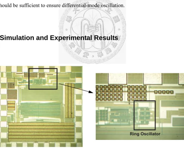
Fig. 3.10 Microphotograph of the fabricated differential four-stage dual-delay
path ring oscillator. 44
Fig. 3.11 Simulated tuning range. 46
Fig. 3.12 Post-simulation results. 46
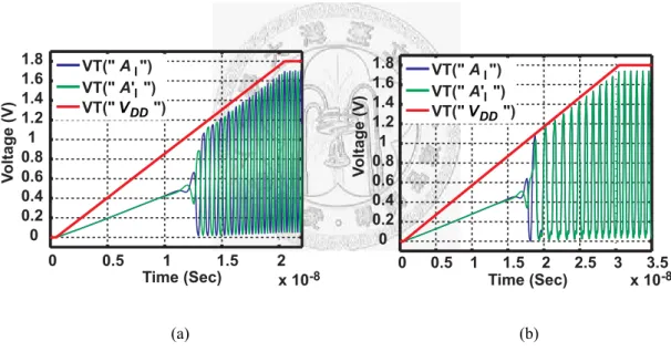
Fig. 3.13 Measurement setup. 47
Fig. 3.14 (a) The sequential VDD signal with slow ramp up slope and fast ramp up slope. (b) Measured output waveform of the ring oscillator. (b) Zoom
in of the output waveform. 47
Fig. 3.15 Measured tuning range. 49
Fig. 3.16 Measured output spectrum. 50
Fig. 3.17 Measured output phase noise. 50
Chapter 4
Fig. 4.1 A conventional Σ-Δ fractional-N frequency synthesizer. 54 Fig. 4.2 Proposed frequency synthesizer architecture. 56
Fig. 4.4 Nonideal model of subcircuits in delay line 1. 59 Fig. 4.5 (a) Architecture of a multiphase fractional division modulator. (b)
Linear model of the integrator. 63
Fig. 4.6 (a) Architecture of the proposed digital control circuit with re-quantized Σ-Δ modulator. (b) Linear model of the re-quantized Σ-Δ modulator. 67
Fig. 4.7 Behavioral simulation result of re-quantized Σ-Δ modulator output signal p[k], without adding constant integer 16. 73
Fig. 4.8 (a) Example of data weighted averaging algorithm. (b) Example of data weighted averaging algorithm with increased index. 76
Fig. 4.9 Architecture of the proposed digital control circuit with DEM block. 80
Fig. 4.10 Linear model of a multiphase compensation Σ-Δ frequency
synthesizer. 80
Fig. 4.11 Behavioral model of the proposed multiphase compensation Σ-Δ
fractional-N frequency synthesizer. 81
Fig. 4.12 Multiphase compensation with ideal delay units. 82 Fig. 4.13 Multiphase compensation with 20% gain error in delay units. 83 Fig. 4.14 Multiphase compensation with multiphase mismatch σm/τ = 40%. 84 Fig. 4.15 Schematic of the ith subcircuit in delay line 1, and the driver circuit. 86
VIII
Fig. 4.16 Architecture of the multi-modulus divider. 88
Fig. 4.17 PFD-CP nonlinear I/O characteristic. 89
Fig. 4.18 Architecture of phase frequency detector, and the constant current
pulse circuit. 89
Fig. 4.19 (a) Third-order passive loop filter of frequency synthesizer.
(b) Second-order passive loop filter of delay-locked loop. 92
Fig. 4.20 Die photo of the frequency synthesizer. 93 Fig. 4.21 Output spectrum of the frequency synthesizer. 94 Fig. 4.22 Phase noise measurement results, without multiphase compensation
(light) and with multiphase compensation (dark). 95
Fig. 4.23 Measurement results of output phase noise, with Vc manually set to
0.7 V. 96
Chapter 5
Chapter 6
List of Tables
Chapter 1
Chapter 2
Chapter 3
Table 3.1 Transistors size. 45
Table 3.2 Performance summary of the experiment results. 51
Chapter 4
Table 4.1 Frequency synthesizer parameters. 82
Table 4.2 Measured performance summary. 98
Chapter 5
X
Chapter 6
Chapter 1 Introduction
1.1 Motivation and Research Goals
The rapid growth of network communication has greatly increased the demand for low-cost and high-performance systems in recent years. Ring oscillators have been widely employed in clock generators and frequency synthesis for their small die size and multiphase outputs.
To increase the oscillation frequencies, dual-delay path ring oscillators are often implemented to explore the maximum frequency levels. However, there are two oscillation modes in four-stage dual-delay path ring oscillators, which might spoil the function of the clock generators and frequency synthesis. For more insight of dual-path ring oscillators, mathematical analysis and demonstrations including the two oscillation mode in a four-stage dual-delay path ring oscillator is presented.
High performance frequency synthesis that requires high-loop bandwidth and low output
phase noise, low spurious tones are demanded by many systems, such as WCDMA transceivers or in-loop modulation systems. Although, Σ-Δ fractional-N frequency synthesis resolves the trade-off between loop bandwidth and input reference frequency, the high-pass quantization noise still limits the performance. Further, quantization noise suppression methods such as multiphase compensation or DAC compensation causes in-band noise and spurious tones due to nonideal element mismatch. To overcome these problems, a multiphase compensation method with dynamic element matching technique in a Σ-Δ fractional-N frequency synthesizer is proposed.
1.2 Thesis Overview
This thesis is divided into five chapters. In Chapter 2, an overview of conventional ring oscillators is introduced, including the small-signal linear model approximation of ring oscillators and the criterion of oscillation. Further, a linear model of fractional-N frequency synthesis and a brief introduction of the concept of quantization noise suppression are also given in this chapter.
A dual-delay path ring oscillator is presented in Chapter 3. The oscillation frequency increment due to additional-delay paths in ring oscillators is firstly derived. Further, the
and demonstrated.
Chapter 4 interprets the architecture of the proposed Σ-Δ fractional-N frequency synthesizer. Basic concept about the multiphase compensation method is firstly provided.
Nonideality about the multiphase element mismatch is also discussed. To solve the nonideal effects, a delay line structure and digital control circuit with dynamic element matching technique are proposed. Behavioral model and analysis are also given.
Experimental results are provided in the end of this chapter
Finally, conclusions of this work are drawn in Chapter 5.
Chapter 2
Basic Concepts
This chapter introduces an overview of ring oscillators and Σ-Δ fractional-N frequency synthesizers, including multi-stage noise shaping (MASH) Σ-Δ modulators, a linear model for fractional-N frequency synthesizers and the concept of quantization noise suppression.
2.1 Ring Oscillators
( )A N (A )1 (A )2 (A )4
Figure 2.1 A conventional differential N-stage ring oscillator
Figure 2.1 shows a conventional differential N-stage ring oscillator, a ring oscillator consists of a number of gain stages in a loop. The oscillation frequency is determined as 1/(2NTd), where N is the number of stages and Td is the large signal delay time of a delay
cell.
-gm,i Vin
CL Ro
Ii
Vout
Figure 2.2 Half circuit small-signal model of a delay cell.
Figure 2.2 shows the half circuit small-signal linear model approximation of a single-delay cell in figure 2.1. Vin and Vout are the input and output signals, respectively.
gm,i represents the transconductance of the input device, Ii is the output current of the input device which flows through the loadings CL and Ro, where CL and Ro represents the total capacitance and the equivalent resistance at the output node, respectively. The transfer function H(jω) between Vin and Vout of a delay cell can be derived as
out o
m i
in 1 o L
V R
H(j ) g
V - , +j R C
ω = = ⋅
ω , (2.1)
and
-
o L
H(j ) - -tan ( R C )1
∠ ω = π ω . (2.2)
According to Barkhausen criterion of oscillation [1], the ring oscillator would oscillate if open loop has unity voltage gain, i.e.,
m,i o
2 o L
1 1
1
N
N g R
H(j )
+( R C )
⎛ ⋅ ⎞
⎜ ⎟
ω = ⇒⎜⎝ ω ⎟⎠ =
, (2.3)
and have a phase shift of 2π or a multiple of 2π. For a N-stage ring oscillator in a stable oscillation state, each stage contributes a same amount of phase shift. Furthermore, let -(π+φ) represent the phase shift of a single stage (2.2), the total phase shift around the loop will be -(π+φ) N=- 2nπ if N is an odd number, or -(π+φ) N-π=- 2nπ if N is even, where n is a positive integer. Thus
-1
osc o L
tan ( R C ) N
φ = ω = π . (2.4)
Therefore, the oscillation frequency can be expressed as
osc
o L
tan( )
= N R C
π
ω . (2.5)
By combing (2.3) and (2.5), the criterion for oscillation can be rewritten as
m,i o
g R =sec( ) N
⋅ π (2.6)
In summary, a N-stage ring oscillator must satisfy the conditions in (2.4) and (2.3), and the oscillation frequency will be as derived in (2.5). If the number of stages in the ring increases the oscillation frequency decreases, shown in (2.5). It should be noted, the derivation so far is a first-order linear approach. In real circuits, as the oscillation amplitude increases the oscillator leaves its linear region and becomes a nonlinear system.
Since the equivalent output resistance, loading capacitance and the transconductance all varies during transient, the oscillation frequency no longer matches equation (2.5) but equals to the large-signal value 1/(2NTd). However, rather than the absolute oscillation frequency, we can capture the tendency of oscillation frequency with respect to N, Ro and CL in real circuits.
2.2 Σ-Δ Fractional-N Frequency Synthesizers
2.2.1 Multi-Stage Noise Shaping (MASH) Σ-Δ Modulators
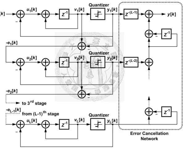
Z-1
u1[k] v1[k] y1[k] Quantizer x[k]
Z-1
u2[k] v2[k] y2[k] Quantizer -e1[k]
Z-1
uL[k] vL[k] yL[k] Quantizer -e2[k]
from (L-1)th stage to 3rd stage -eL-1[k]
Z- (L-1)
Z-1
Z- (L-2)
Z-1 y[k]
Error Cancellation Network
Figure 2.3 A high-order MASH Σ-Δ modulator.
yi[n]
vi[n]
ei[n]
Quantizer
Figure 2.4 Equivalent model of a quantizer.
Recently, fully digital Σ-Δ modulators have become the main building blocks in Σ-Δ fractional-N frequency synthesizers for divider control. Σ-Δ modulators can be classified into two main categories [2] [3]. One of them is single-loop type Σ-Δ modulators, and the other is multi-stage noise shaping Σ-Δ modulators or MASH. MASH structure enables higher-order modulators without reducing the dynamic range, while in single loop type modulators, higher-order modulators requires careful design on signal condition around the loop for stability consideration, which in turn reduces the input dynamic range. Figure 2.3 shows an example of a Lth-order MASH structure [4]. The input and output signals are represented by x[k] and y[k], respectively. ui[k], vi[k] and yi[k] are the intermediate node signals. In figure 2.4, shows an equivalent linear model of the quantizers in figure 2.3.
Quatizaers are now represented as the addition of vi[k] with an error term ei[k], where ei[k]
represents the error sequence by quantization. Now, from figure 2.3, the output signal y[k]
can be derived as
-L -1 -(L-1) -1 -1 -(L-2) -1
1 1 2
-1 -1 -1 L-1
L-1 L
-L -1 L
L
s L n
y(z)=x(z) z +e (z) (1-z ) z +(-e (z) z +e (z) (1-z )) z (1-z )+
+(-e (z) z +e (z) (1-z )) (1-z )
=x(z) z +e (z) (1-z )
=x(z) H (z) y(z)
+e (z) H (z)
= y(z) y(z)
⋅ ⋅ ⋅ ⋅ ⋅ ⋅ ⋅ ⋅ ⋅ ⋅
⋅ ⋅ ⋅ ⋅ ⋅ ⋅
⋅ ⋅
⋅ ⋅
, (2.6)
Hs(z) and Hn(z) represents the signal transfer function (STF) and noise transfer function
(NTF), respectively. From (2.6), since Hs(z) equals to unity, the output signal is shown to contain the input signal plus an error term. The output error term is the quantization error eL(z) shaped by the filter (1-z-1)L. By assigning q(z)=eL(z)Hn(z), the power spectrum density of the output quantization noise Sq can be derived
L L
- 2π 2 2
1 j fT L 2 L
q e e
S (f) S (f) ( -e= ⋅ ) = S (f) ( sin( fT))⋅ π . (2.7)
if the πf is small and 1 << T, (2.7) can be further written as
L
L
2
10 10
2
20 2 10
L
q e
e
S (f) S (f) ( fT)
L log Tf + log S (f)
= ⋅ π
= ⋅ ⋅ π ⋅
. (2.8)
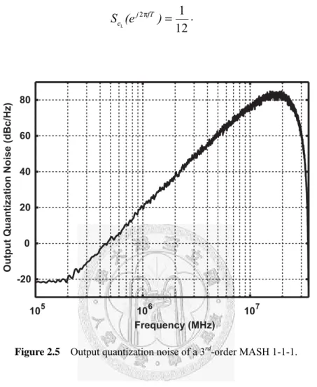
Several assumptions were made about the quantization error eL [4]. Ideally, eL is white and uniformly distributed between 0 and 1, and can be modeled as an additive white noise with magnitude 1/12. Thus the power spectrum density of eL can be described as
L
2 1
12
j fT
S (ee π )= . (2.9)
105 106 107
-20 0 20 40 60 80
Output Quantization Noise (dBc/Hz)
Frequency (MHz)
Figure 2.5 Output quantization noise of a 3rd-order MASH 1-1-1.
From (2.8) and (2.9), the output quantization noise q(z) is found to have of a 20L dB/decade slope in spectrum at low offset frequencies. In figure 2.5, shows the simulation results of the output quantization noise spectrum Sq of a 3rd-order MASH 1-1-1 modulator, with dc input and T = 28.6 nsec (inverse of 35 MHz). A 60 dB/decade noise increment can be clearly observed. The simulation is executed in a behavioral model implemented in CPPsim [5].
2.2.2 A Linear Model for Fractional-N Frequency Synthesizers
Ι Φout
q[k]
2Tπ
H(f)
jf KV
Nnorm
1 1
(t) Φin[k]
z-1 1- z-1
T
2π Φdiv[k]
Φn[k] PFD
CP
Loop
Filter VCO
Divider
z=e j2πfT
Figure 2.6 A linear model for fractional-N frequency synthesizers.
Traditional models of PLL analysis assumes a static divide value, which is not straightforward for fractional-N synthesizers since their divide value dynamically changes according to the output of Σ-Δ modulators. In [6], a linear model for fraction-N synthesizer especially Σ-Δ types has been analyzed and demonstrated, shown in figure 2.6. Effect of quantization noise as well as the influence of various noise sources on the frequency synthesizer phase noise can be analyzed by this linear model.
In figure 2.6, T, I and Kvco represents the period of the input reference clock, the gain of the charge pump and the gain of the voltage control oscillator (VCO), respectively. H(f) is the loop filter constructed of either passive or active devices. Further, Φout(t) represents the
phase deviation at the frequency synthesizer output. To be noted, this is not the exact phase of the output, which is
nom out
2π ⋅ f ⋅ + Φt (t). (2.10)
In further discussions the nominal phase 2πfnomt will not be included, since it is the phase deviation that we are interested in. Furthermore, with considering the sampling characteristic of the divider, Φdiv[k] represents the phase deviation of the divider output.
Similarly, Φin[k] represents the phase deviation of the input reference clock which equals to Φin(kT). Moreover, q[k] represents the output quantization noise produced by the Σ-Δ modulator that causes incremental change in the frequency of the divider output
vco vco
div
nom
f f
f = N[k] = N +q[k], (2.11)
N[k] is the division value of the divider, and Nnom is the nominal division value [6]. fvco and fdiv represents the out frequency of VCO and divider, respectively. By integrating q[k]
results to the phase deviation value Φn[k] caused by output quantization noise. Indicated in figure 2.6, the operation of the divider, on one hand samples the continuous-time signal Φout(t), and on the other hand integrates the output quantization noise q[k] of Σ-Δ
modulator. Then by adding the sampled value with the integrator output together and divide by Nnom, results to the feedback signal Φdiv[k]. Finally by figure 2.6 the open-loop transfer function A(f) can be expressed as
div VCO
ref nom
1 1
2
A(f)= = I H(s) K
j f N
⎛ ⎞
⎛ ⎞
ΦΦ ⎛⎜⎝ π⎞ ⋅⎟⎠ ⎜⎝ ⎟⎠⎝⎜ ⎟⎠
. (2.12)
Since there is a jf term in the denominator of A(f), it has a low pass nature with infinite gain at dc. With (2.12) the closed-loop transfer function G(s) can be written as
out
ref 1
G(f) A(f)
+A(f)
= Φ =
Φ . (2.13)
G(f) equals to 1 at dc and approximates 0 as frequency increase infinitely, this implies that
G(f) is a low-pass filter.
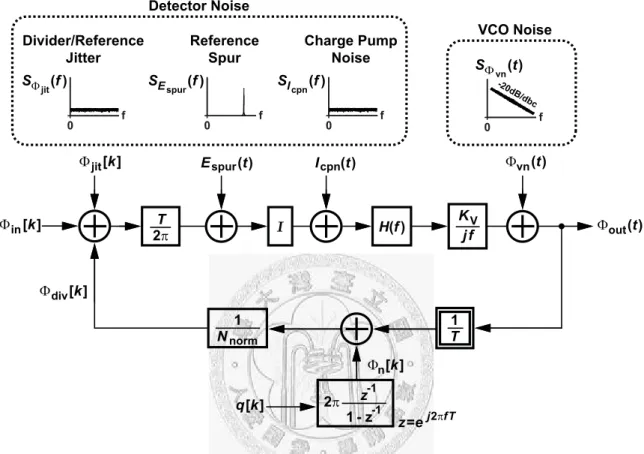
2.2.3 Effect of Various Noise Sources in Frequency Synthesizers
Ι Φout
q[k] 2Tπ
H(f )
jf KV
Nnorm
1 1
(t) Φin[k]
z-1 1- z-1
T
2π Φdiv[k]
Φn[k] Icpn(t) Espur(t)
Φjit[k] Φvn(t)
0 f
SΦ
vn(t) VCO Noise
-20dB/dbc
0
SΦ
jit(f )
Divider/Reference Jitter
f 0
Reference Spur
f
0
SI
cpn(f )
Charge Pump Noise
f
Detector Noise
SE
spur(f )
z=e j2πfT
Figure 2.7 A linear model of fractional-N frequency synthesizers including various noise sources.
Indicated in figure 2.7, besides quantization noise there are other noise sources in a PLL based frequency synthesizers such like divider/reference jitter, Φjit[k] corresponds to noise-induced variations in the transition time of the input reference clock or divider output signal. Periodic reference spur, Espur(t) caused by current mismatch in charge pump or other affect such as charge injection and charge sharing. Charge pump noise, Icp(t) induced by the transistors that construct the charge pump circuit. Finally, VCO noise, Φvn(t)
caused by intrinsic noise of the VCO and voltage noise at the output of the loop filter.
As shown in figure 2.7, the noise sources have been lumped up into two categories, VCO noise and detector noise. This comes from the reason that divider/reference jitter, reference spur and charge pump noise all interacts with a low pass filter to the frequency synthesizer output. On the contrary VCO noise interacts with a high pass filter to the frequency synthesizer output.
From (2.13) and figure 2.7, the detector noise, VCO noise and their effect on the frequency synthesizer output can be derived as follow
out Detector Noise out Divider/Reference jitter out Reference Spurs out Charge Pump
S (f)Φ =S (f)Φ +S (f)Φ +S (f)Φ , (2.14)
where
out jit
out spur
out cpn
2 Divider/Reference Jitter nom
2 Reference Spurs nom
2 nom
Charge Pump
2 2
E
I
S (f) T N G(f) S (f)
S (f) N G(f) S (f)
S (f) N G(f) S (f)
I
Φ Φ
Φ
Φ
⎧⎪ = ⋅ ⋅
⎪⎪
= π ⋅ ⋅
⎨⎪
⎪ = π ⋅
⎪⎩
. (2.15)
and
out vn
2 VCO Noise 1
S (f)Φ = -G(f) S (f)Φ . (2.16)
Further, from (2.7), (2.13) and figure 2.7, the effect of Σ-Δ modulator output quantization noise on the frequency synthesizer output can be obtained as
( )
o out
L ut
- 2 2 2
Quantization Noise Quantization Noise - 2
2 2 2( -1)
1
1
1 2 2
j fT
j f q
Φ
T
L e
S (f) T G(f) e S (f)
T e
T G(f) ( ) sin( fT)
S (f) S (f)
T
-
π
Φ = ⋅ ⋅ 2π π
= ⋅ ⋅ ⋅ π ⋅ π
. (2.17)
Shown in (2.17), the effect of output quantization noise of an Lth-order Σ-Δ modulator on the synthesizer output reduces in order by one. This come form the integrating operation of divider.Finally, the total output noise can be derived by summing up (2.14), (2.16) and (2.17)
out Total Noise out Detector Noise out VCO Noise out Quantization Noise
S (f)
Φ= S (f)
Φ+ S (f)
Φ+ S (f)
Φ . (2.18)T G(f )
2π fo
1-G(f ) 2πNnormG(f )
2Tπ
Ι1
Φn[k] Φout(t) Φout(t) Φtn,pll(t)
En(t) Φvn(t) Icpn(t)
Espur(t) Φjit[k]
Noise Analysis
eL[k] Hn(z)
NTF q[k]
Σ-Δ Modulator
0 f
SΦ
vn(t)
VCO Noise
-20dBc/dec
0 f
SE
n(t)
Detector Noise
0 f
Sq(e j2πfT) Delta-Sigma Noise
z-1 1-z-1
fo fo
z=e j2πfT
Figure 2.8 A parameterized model of a Σ-Δ synthesizer.
104 105 106 107
-160 -150 -140 -130 -120 -110 -100 -90 -80 -70 -60
Frequency (MHz)
Output Phase Noise (dBc/Hz)
Quantization Noise VCO Noise
Detector Noise Total Noise
Figure 2.9 Output phase noise of a frequency synthesizer.
Figure 2.8 shows a parameterized model of Σ-Δ fractional-N frequency synthesizers,
including quantization noise, VCO phase noise and detector noise and their effect on the frequency synthesizer phase noise performance. With the aid of various noise spectrum derived earlier, figure 2.9 shows an example of a frequency synthesizer output phase noise diagram. A frequency synthesizer with 70 kHz bandwidth and 35 MHz input reference clock is examined. In figure 2.9, the blue line represents the impact of VCO noise at the synthesizer output, by modeling VCO noise as a -20 dB/decade slope curve with a spot noise of -130 dBc/Hz at 1 MHz offset frequency. The actual VCO deviates from the -20 dB/decade rolloff at low frequencies due to 1/f noise, and at high frequencies due to a finite noise source. The green line represents the detector noises, in this example reference spurs is neglected and the detector noise is modeled as a -90 dBc white noise. As mentioned before the detector noise interacts with a low pass filter before reaching the synthesizer output. Shown in figure 2.9, the influence of detector noises dominates at low offset frequencies, and the influence of VCO and quantization noise dominates at high offset frequencies.
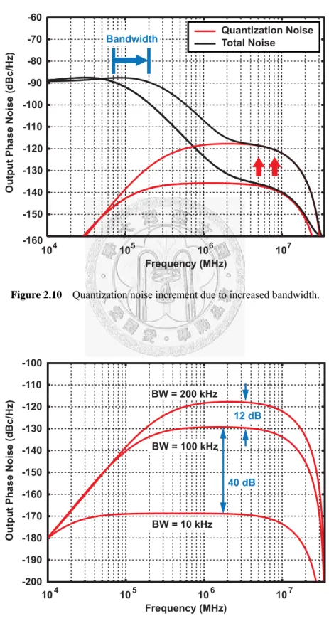
2.2.4 Concept of Quantization Noise Compensation
104 105 106 107
-160 -150 -140 -130 -120 -110 -100 -90 -80 -70 -60
Frequency (MHz)
Output Phase Noise (dBc/Hz)
Quantization Noise Total Noise
Bandwidth
Figure 2.10 Quantization noise increment due to increased bandwidth.
104 105 106 107
-200 -190 -180 -170 -160 -150 -140 -130 -120 -110 -100
Output Phase Noise (dBc/Hz)
Frequency (MHz) BW = 10 kHz BW = 100 kHz BW = 200 kHz
40 dB 12 dB
Figure 2.11 Synthesizer output quantization noise with BW=10 kHz, BW=100 kHz and BW=200 kHz.
Figure 2.10 shows an example of the effect of 3rd-order MASH modulator output quantization noise on frequency synthesizer output phase noise, while increasing the loop bandwidth of frequency synthesizer. The input reference clock is 35 MHz, VCO noise model and detector noise model are the same as those applied in figure 2.9. As shown in figure 2.10, the quantization noise increases with a 40 dB/decade slope at low offset frequencies. With an increment in bandwidth from 70 kHz to 200 kHz which is about 0.45 decade, causes an increment in quantization noise of about 0.45 (decade) × 40 (dB/decade)
= 18dB. Moreover, in frequency synthesizers that utilizes 2nd-order MASH modulator, the quantization noise increases with a 20 dB/decade slope at low offset frequencies on the synthesizer output. Thus, increasing bandwidth from 70 kHz to 200 kHz, causes quantization noise to rise of about 0.45 (decade) × 20 (dB/decade) = 9 dB. Note in figure 2.10, only the quantization noise and the total noise curves are depicted, detector noise and VCO noise are not shown for clearance. Figure 2.11 shows the effect of quantization noise on frequency synthesizer output with difference loop bandwidths.
104 105 106 107 -160
-150 -140 -130 -120 -110 -100 -90 -80 -70 -60
Frequency (MHz)
Output Phase Noise (dBc/Hz)
Quantization Noise Total Noise
Compensation No Compensation
104 105 106 107
-160 -150 -140 -130 -120 -110 -100 -90 -80 -70 -60
Frequency (MHz)
Output Phase Noise (dBc/Hz)
Quantization Noise Total Noise
Compensation No Compensation
(a) (b)
Figure 2.12 (a) Quantization noise reduction due to compensation. (b) Comparison between low bandwidth
synthesizer and high bandwidth synthesizer with quantization noise compensation method.
In applications such as WCDMA or in-loop modulation systems that require large-loop bandwidth frequency synthesizers, the quantization noise might spoil the phase noise performance at high offset frequencies. For this reason, several researches have been reported to compensate the quantization noise [7]-[14]. Figure 2.12(a) shows an example of ideally reducing quantization noise due to DAC or multiphase compensation methods.
As indicated in figure 2.12(b), an 18 dB reduction on quantization noise, enables the loop bandwidth to increase from 70 kHz to 200 kHz, without spoiling phase noise performance at high offset frequencies. However, nonideal effect such as element mismatch in the compensation circuit causes in-band noise and spurious tones. To overcome these problems, a multiphase compensation Σ-Δ fractional-N frequency synthesizer with
dynamic element matching (DEM) techniques for mismatch linearization is proposed in chapter 4.
Chapter 3
The Design and Analysis of Dual-Delay Path Ring Oscillators
This chapter introduces the design and analysis of dual-delay path ring oscillators. With mathematical analysis, the oscillation frequency increment due to additional-delay paths is derived. Further, the two oscillation mode in differential four-stage dual-delay path ring oscillators is analyzed and demonstrated.
3.1 Introduction
Ring oscillators have been widely employed in most of clock generators and frequency synthesis for their useful features such as small die size, multiphase outputs, as well as easy integration in a standard CMOS process. Because the oscillation frequency of ring oscillators is determined by the propagation delay time of each delay cells, single-loop ring oscillators lack for high oscillation frequency. Several techniques have been reported to
explore the maximum frequency levels of ring oscillators, such as sub-feedback loops [15], output-interpolation methods [16], multiple-feedback loops [17] and dual-delay paths [18]-[20].
A I
in1+
in2+
in1- in2-
in1+
in2+
in1- in2-
in1+
in2+
in1- in2-
in1+
in2+
in1-
A` I in2-
B I
B` I
A Q
A` Q
B Q
B` Q
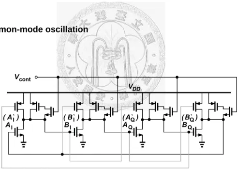
Figure 3.1 A differential four-stage dual-delay path ring oscillator.
In this work, a differential four-stage dual-delay path ring oscillator, in figure 3.1, was implemented for its high oscillation frequencies and its improvement of phase noise performance. However, there happens to be two operation modes in the oscillator, named differential-mode oscillation and common-mode oscillation. The initial conditions affect the operation of the dual-delay path ring oscillator. The main difference of the two operation modes is the output waveform characteristic. Instead of typical differential output signals, the outputs of a delay cell becomes in-phased. Furthermore, the oscillation frequency in either mode is different.
3.2 Oscillation Frequency in Multiple-Delay Path Ring Oscillators
Vin1 Vout
CL Ro
I1 Vin2
-gm2 I2 M2
M1 -gm1
Vin1
0 90
IT
Vout Vin2
I2
I1 α
θ φ
(a) (b)
Figure 3.2 (a) Half circuit small-signal model of a dual-delay path delay cell. (b) The phasor diagram of the
signals Vin1, Vin2, Vout and currents I1, I2.
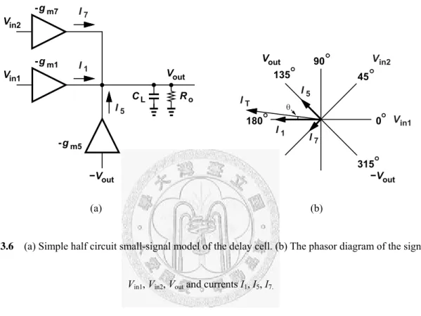
Figure 3.2(a) shows the half circuit small-signal model of a delay cell in dual-delay path ring oscillators. Dual-delay path means both the additional-delay path and the main-delay path exits in the same ring oscillator. The additional-delay path should be introduced in a way which decreases the delay time of a single delay cell, as a result the oscillation frequency increases. The inverters M1 and M2 are the input devices of the main-delay path signal Vin1 and the additional-delay path signal Vin2, respectively. gm1 and gm2 represent the transconductance of the inverters M1 and M2, respectively. CL and Ro represent the total loading capacitance and the equivalent output resistance at the output node, respectively. I1
and I2 are the output currents of the inverters M1 and M2, respectively. The phasor diagram of the voltage signals Vin1, Vin2, Vout and currents I1, I5 in a stable oscillation state is illustrated in figure 3.2(b) [21]. The phase of Vin1 is set as zero for the reference. The phase of Vout with respect to Vin1 is -(π+φ), where φ=π/N in a N-stage ring oscillator. The phase of Vin2 with respect to Vout is α. IT is the vector summation of I1 and I2. The resultant phase of IT yields θ degree phase difference with respect to I1 and is indicated in figure 3.2(b).
Vin1
0 90
IT
Vin2
I2 I1
in1,I
V I2,I I1,I
I +1,Q I2,Q V out in2,I
V ,
φ+θ
in1,Q
V , V in2,Q
Figure 3.3 Redrawn phasor diagram of figure 3.2(b).
Figure 3.3 is the redrawn phasor diagram of figure 3.2(b). The main-delay path signal Vin1 is splitted into two signal components Vin1,I and Vin1,Q, where Vin1,I is in parallel with Vout and in orthogonal to Vin1,Q. The relation of Vin1,I and Vin1,Q with respect to Vin1 can be expressed as
in1,I in1
2 in1,Q in1
-j
j( - )
V V e cos
V V e sin
φ π φ
⎧ = ⋅ ⋅ φ
⎪⎨
= ⋅ ⋅ φ
⎪⎩
. (3.1)
Similarly, the additional-delay path signal Vin2 is also splitted into two signal components Vin2,I and Vin2,Q, where Vin2,I is in parallel with Vout and in orthogonal to Vin2,Q. The relation of Vin2,I and Vin2,Q with respect to Vin2 can be expressed as
in2,I in2
2 in2,Q in1
j
-j( -α)
V V e cos
V V e sin
α π
⎧ = ⋅ ⋅ α
⎪⎨
= ⋅ ⋅ α
⎪⎩
. (3.2)
The transfer function H(jω) between Vin1 and Vout of a single stage delay cell can be found as follows. The output signal Vout can be described as
(
o L)
out IT R //C
V = ⋅ , (3.3)
where (Ro//CL) is the output node loading. The equivalent output current IT can be derived as
T 1 2
2 2 θ
2 m1 m2
i m
T n1 1 m 2 j
I
I I I
V g g g g cos( - - ) e
-
= +
= ⋅ + + π α φ ⋅ , (3.4)
By combing (3.3) and (3.4), the transfer function H(jω) can be written as
2 2 θ
out o
2 m1 m2
m1 m
in1 o L
2 1
V j R
H(j ) g g g g cos( ) e
V - - - j R C
ω = = + + π α φ ⋅ ⋅
+ ω (3.5)
1
o L
H(j ) - -(tan ( R C )- - )
∠ ω = π ω θ . (3.6)
According to Barkhausen criterion of oscillation [1], the ring oscillator would oscillate if loop has unity voltage gain, i.e.,
2 2
2 m1 m2
m1 m o
2 o L
1 2 1
1
g g g g cos( - - ) R
H(j )
( R C )
+ + π α φ ⋅
ω = ⇒ =
+ ω
(3.7)
and have a phase shift of 2π or a multiple of 2π. Thus, from (3.6) the oscillation frequency can be expressed as
osc
o L
1 tan( )
ω = R C ⋅ φ + θ , (3.8)
with further derivation the oscillation frequency can be rewritten as
m1,Q m2,Q
m1 m2
osc
o L m1 m2 o L m1,I m2,I
1 g sin g sin 1 g g
R C g cos -g cos R C g -g
φ + α +
ω = ⋅ = ⋅
φ α , (3.9)