延攬人才工作報告表
工作期間,共計發表 17 篇國際 SCI 論文與研討會論文 15 篇 (期刊論文資訊附加於報告表後
半)。主要可分成四個主題: 1. 液晶聚合物薄膜光子晶體的光開關; 2.膽固醇液晶薄膜的
選頻與邏輯閘; 3.螺旋光的產生與應用; 4.光開關原件與節能智慧窗。英文摘要如下:
1.
液晶聚合物薄膜光子晶體的光開關(Bichromatic optical switch of diffractive light from a BCT photonic crystal based on an azo component-doped HPDLC)
This study demonstrates all optical switches between the four diffractive light levels of a body-centered tetragonal photonic crystal. The sample is based on holographic polymer-dispersed liquid crystals that are fabricated using a two-beam interference with multiple exposures. The switching mechanism bases on the effective index modulation of the PC that contains a liquid crystal/azo-dye mixture could be controlled by two pumping laser beams. The switching time between the blue-laser-pumped and the blue-and-green-laser-pumped levels is fast. The study also discusses the switching time of the various levels.
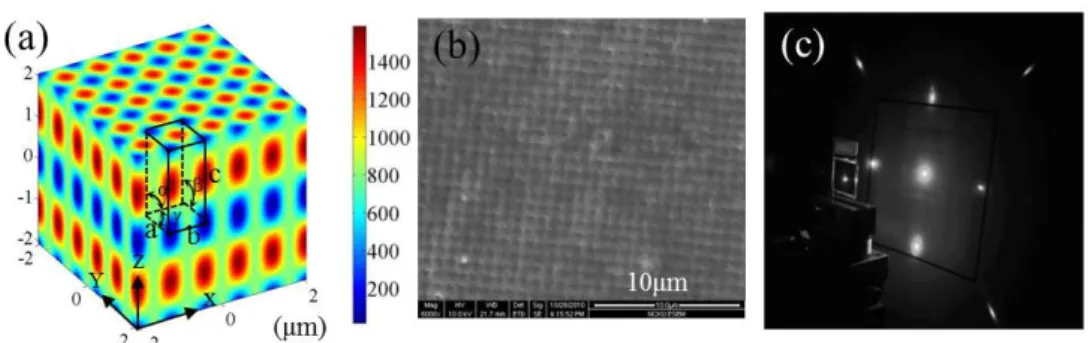
Fig. 1. Simulated intensity profile of interference region, (b) top-view SEM image of HPDLC profile, and (c) far field view of the diffraction image of the BCT sample.
Figure 1(a) gives the 3D simulated intensity profile of the interference region which is constructed using two-beam interference with four exposures. The figure also gives the illustration of a unit BCT cell. As the sample is exposed to the interference pattern, the photoreactive monomers diffuse to the bright regions (red regions in Fig. 1(a)) of the interference pattern, while the liquid crystal molecules consequently congregate in the dark regions (blue regions in Fig. 1(a)) which locate at the lattice point of the PC. By removing the LCs, figure 1(b) shows the top-view scanning electron microscope (SEM) image of the sample in which the polymer surface structure contains a matrix (polymer-rich region) as well as voids (LC-rich region). The primitive cell of the BCT structure has the dimension a = b ≠ c. The a and c lattice constants are ~0.813 ± 0.016 μm and ~3.416 ± 0.068 μm, respectively, and the diameter of the voids that contain the LC droplets is ~0.25 μm [18]. Figure 1(c) presents the far field diffraction image from the sample. The maximum diffraction efficiency of the 1st-order diffractive beams is approximately ~ 15%.
Fig. 2. Experimental setup used to measure the optical switch properties of a HPDLC-based PC. D: detector; S: shutter; A: aperture; CF: color filter; BS: beam splitter.
Figure 2 shows the experimental setup used to measure the optical switch properties of the BCT PC. A TE-polarized Ar+ laser (green, λ = 514.5 nm, intensity = 400 mW/cm2) beam and a diode laser (blue, λ = 403 nm, intensity = 100 mW/cm2) illuminate the sample at 30°, whereas a He-Ne laser is used to probe the BCT sample. In the experiment, shutters are used to control the exposure time of the green and blue laser beams. An aperture and a color filter were placed behind detector 2 to prevent laser light reflection. The pumping conditions of non-exposure and exposure to green, blue and green, and blue laser beams are simplified into OFF, ONG, ONB+G, and ONB, respectively, for convenience.
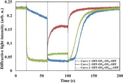
Fig. 3. Intensities of the diffraction beam when the samples were pumped by various laser beam combinations. The pumping conditions of non-exposure and exposure to green, blue and green, and blue laser beams are simplified into OFF, ONG, ONB+G, and ONB for convenience.
Figure 3 shows the diffraction beam intensity when the samples are pumped using a blue and/or a green beam. The exposure time is set at 40 s. Curves 1 to 3 in Fig. 4 represent the diffraction intensities of the He-Ne laser beam from the BCT PC, which is subjected to the OFF-ONG-ONB-OFF, OFF-ONB-ONG-OFF, and OFF-ONB-ONB+G-OFF laser pumping process. As mentioned above, the intensity of the diffraction beam depends on the cis isomer concentration shown in Eq. (2). The intensity weakens when the cis isomer concentration increases upon exposure to either green or blue laser beams. However, the wavelength of the pumping blue laser is close to the absorption band that generates a higher cis isomer concentration than that of the green laser. The high cis isomer concentration induces the transition of the LCs in the voids into an isotropic state. The diffraction intensity is relatively low compared with that pumped by the green laser. As the first pumping green laser is replaced by the blue laser, the diffraction intensity rapidly drops (curve 1). Similarly, the intensity increases as the pumping laser beam sequence is inverted (curve 2). The diffraction intensity rapidly decreases and increases when the blue pumping
laser beam is replaced by the green one. However, a comparison of the OFF-ONG and ONB-ONG paths shows that the ONG levels are different, with the ONG level of the latter requiring a few seconds to recover to the former. This phenomenon becomes apparent when the exposure time to the blue laser exceeds several minutes. Thus, the thermal effect may be affecting the order parameter of the LCs. The newly created level is constant until the heat dissipates or even when no external disturbance exists. When the green laser beam is added to the pumping blue laser, the diffraction light intensity increases (curve 3). This result is expected because the green laser not only increases the trans isomer concentration but also promotes the organization of the host LCs by the newly transformed trans isomers. In other words, the trans isomer produced under the green laser beam reconverts the LC structure to the initial configuration. This change is temporary and disappears as soon as the green pumping laser is off.
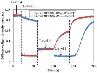
Fig. 4. Upstep and downstep of the levels. One of the curves represents a level up that corresponds to the increase from level 1 to level 4, whereas the other represents a level down that corresponds to the decrease from level 4 to level 1.
For convenience, the intensities of the diffraction beams in these curves can be classified into four levels, namely, level 4 (OFF), level 3 (ONG), level 2 (ONB+G), and level 1 (ONB), according to the exposure conditions. Figure 6 shows the level upsteps and downsteps by combinations of exposures to the two lasers. One of the curves represents a level up that corresponds to the raising of level 1 to level 4 under ONB-ONB+G-ONG-OFF exposure. The other curve represents a level down that corresponds to the decrease from level 4 to 1 under OFF-ONG-ONB+G-ONB exposure. The contrast of levels 4, 3, and 2 are 7.5, 5–6, and 2, respectively, as compared to that of level 1. As seen from the curves, the ONG level is sensitive to the thermal effect during laser optical pumping. Hence, the immediate contrast of the ONG level depends on the path used to reach this level.
Final Level 1 (ONB) Level 2 (ONB+G) Level 3 (ONG) Level4 (OFF) Initial Level 1 (ONB) X <600μs ~14s ~29s Level 2 (ONB+G) <800μs X >40s 34s Level 3 (ONG) 200ms 60ms X 27s Level 4 (OFF) 120ms 150ms >40s X
Table 1 gives the summarized switching time between the four levels. The switching times of the levels are affected by the guest dye, the governing factors (i.e., quantum efficiency, absorption cross-section, and rate constant of the thermal
cis-trans back-relaxation), and the thermal effect. The thermal dissipation and phase transition of LCs apparently inhibit the
switching. Thus, the LCs in the ONB-OFF process has a delayed relaxation time during phase transition (curve 1 of Fig. 6). The thermal effect slows down the ONB+G-ONG switching (curve 2 of Fig. 6). Therefore, the ONB-OFF and ONB+G-ONG level transitions that are affected are generally avoided in applications because of their relatively slow switching time. Given the long distance of the trans isomer absorption band from the green laser wavelength, trans isomer production is not efficient. Thus, the overall LC distribution is difficult to change, which results in a relatively slow OFF-ONG switching time. Therefore, the switching times for OFF-ONG, ONB- OFF, and ONB+G-ONG are on the order of tens of seconds. The ONB-OFF switching time can be improved by exposure to the green laser because ONB-ONG transition is faster than that of ONB-OFF. Here, a small amount of trans isomers produced under green laser exposure significantly promotes the recovery of the LC order. In addition, the switching from level 1 (ONB) to level 4 (OFF) in applications can be significantly improved by a short-pulse exposure to green laser. The level recovery from ONB+G to ONG is relatively slow because the ONB+G level contains some
trans isomers. The newly produced trans isomers also do not exert a strong effect. The back processes to levels ONG and OFF are long because LC relaxation from a disordered state to the normal state is required.
6. Conclusion
In conclusion, a four-level optical switching is established using two laser beams that are based on an azo dye-doped HPDLC film. The switching time between the ONB and ONB+G levels is short. Since the electrical switching of nano-sized HPDLCs requires a sufficiently high voltage (~10 V/μm), and is difficult to switch off completely, the optical switching provides us a better switching in these respects. Furthermore, the pumping laser wavelength and intensities can be optimized to increase the contrast ratio of ONB to ONB+G. The CR of the ONB+G-ONG level can be increased by increasing the green laser intensity. The optical switching of PCs based on HPDLC has high potential in electro-optical applications.
2.膽固醇液晶薄膜的選頻與邏輯閘;
(Bichromatic tuning of reflection bands in integrated CLC reflectors for optical switches, gates, and logic)
This study investigates the bichromatic tuning of cholesteric liquid crystal (CLC) reflection bands from reflectors containing azo-chiral dopants. The CLC reflectors are integrated into an optical gate that can be used to modulate output spectra. We also apply the integrated system in optical switching and logic.
Tab. 1. Chemical compositions of the CLC reflectors
The CLC pitch length controls the Bragg wavelength, and the selective reflection wavelength is given as:
λ
=
n p
*
(1)where n = (ne+no)/2; p is the CLC pitch; and λ is the central wavelength of the reflection band. The CLC pitch length is
determined by the concentrations of the guest azo-components and their HTP using the following equation: 1 1 2 2 1 * * p c HTP c HTP = + (2)
The CLC reflectors used in this study have two types of chiral component; one of these components is an azo-chiral dopant with optical tunable HTP. The reflection bands are adjustable. Table 1 shows the concentrations of the chemical compositions in the samples in wt%. The CLC mixture consists of nematic liquid crystal (MDA-00-3461, cleaning temperature of 92 °C, Merck), left-hand chiral dopant (S1011, Fusol materials), and azo-chiral dopant (3c-S/ 3c-R BEAM Corp.). The Ql-3c-S/R series consists of azo-chiral dopants that have right- and left-hand HTP, respectively. Photoisomerization, which is a process in which trans-isomers become cis-isomers and the azo-chiral dopants gradually lose HTP, occurs upon irradiation with a purple laser beam. The cis-isomers revert to trans-isomers and the azo-chiral dopants recover HTP upon irradiation with a green laser beam because photoisomerization is reversible. The pitch length that governs the CLC reflection band is modulated by controlling trans- (or cis-) isomer concentration. Therefore, the reflection bands of azo-chiral-doped CLCs can be bichromatically tuned by exposure to a combination of purple and green laser beams.
The reflection band of sample A measures 700 nm, and the left and right HTPs of the chirals tend to offset each other. The reflection band of sample B measures 400 nm, and the left HTPs are added. The trans-isomer becomes a cis-isomer during photoisomerization, and the azo-chirals lose HTP upon exposure to purple laser light. Hence, the reflection band of sample A can be tuned to 400 nm, whereas the reflection band of sample B can be tuned to 700 nm. These pitch-length changes are called red-shift or blue-shift because they cause reflection bands to approach either infrared or ultraviolet.
Indium-tin-oxide glasses were immersed in a polyvinyl-alcohol solution and baked for 25 minutes at 125 °C to prepare the samples. The surfaces of the glasses were rubbed, and a cell was then built by sandwiching a 20 μm-thick spacer between two glass pieces that were rubbed in opposite directions. The solutions were heated to 80 °C and injected into the cells. The sample CLCs had a planar texture as a result of the homogeneous-alignment pre-treatment in the cells. The 20 μm cell gap was sufficiently thick to ensure that the CLC layers had 50% reflection efficiency and that the optical tuning speed was
adequately slow.
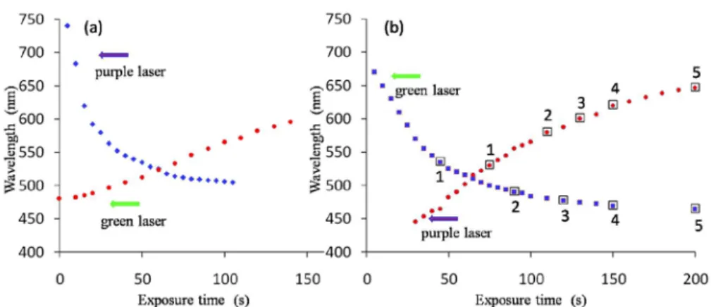
Fig. 1. Central wavelength shift of the CLC reflectors from (a) sample A and (b) sample B upon exposure to green/purple laser beams.
The bichromatic tunabilities of the reflection bands of CLC reflectors were measured. The intensity of the purple and green laser beams was approximately 1.3 mW/cm2. The selected light intensities were not strong enough to tune the reflection bands according to the complete range (from 400 nm to 700 nm) to determine the stable, linear band shift during laser pumping. Figure 1 shows the central-wavelength curves versus the exposure times of samples A and B to the purple and green laser beams. The samples were subjected to purple laser pumping for 300 s and then to green laser pumping to recover the reflection band. The blue-shift in sample A, which has both left- and right-hand HTP chirals, is quick in the first 20 s and slows down after 100 s. The left-hand chiral dominates the structure as resistance from the right-hand chiral disappears. The red-shift is almost linear; however, the reflection band only reverts to 600 nm. The red-shift in sample B, which has two kinds of left-hand HTP chirals, is linear in purple laser pumping. The blue band shift is quick in the first 40 s and subsequently slows down. The recovery curve shows two-segment linear changes at the 700 nm to 530 nm (0 s to 40 s) and 530 nm to 450 nm (40 s to 200 s) bands. Sample A is used to locate the reflection band, whereas sample B is primarily used to reverse the sample A reflection bands, as described in the following section.
Fig. 2. Experimental setup of the optical gate in incident-light switching. The reflection spectra from samples A and sample B are plotted above to show their band-shift directions as they undergo purple- or green-laser pumping.
Figure 2 shows the experimental setup of the optical-gate CLC integrated reflector. A halogen lamp acts as a broadband light source for sample A and is reflected by the parallel-aligned CLC reflectors of samples A and B. The reflected light is absorbed into the spectrometer (Ocean Optics, USB2000). The reflection bands of both CLC reflectors can be
bichromatically tuned individually using the CW DPSS laser (green laser, λ = 532 nm) and a purple laser (λ = 406 nm). The reflection spectra from samples A and B are plotted to show their band-shift directions as they undergo either purple- or green-laser pumping. The exposures to green and purple lasers are defined as the inputs hν0 and hν1, respectively.
Fig.3. (a) The reflection spectra of sample A, sample B, and incident-light output-spectra as the overlap of samples A and B. Incident-light output-spectra switching by controlling the exposure times of the CLC reflectors to the (b) green and (c) purple laser beams.
Figure 3(a) shows the reflection spectra of sample A, sample B, and of the overlap of samples A and B. The central wavelengths of the samples are determined to be between 500 nm to 550 nm. Hence, sample A is pre-exposed to purple light for 50 s, whereas sample B is pre-exposed to purple light for 45 s. The reflection band of sample B is thus shifted by exposure to either the green or purple laser beams. The overlap of the bands from samples A and B varies because the reflection bands of sample B shift, and optical switching is achieved.
Figures 3(b) and 3(c) show the output spectra when sample B undergoes green- and purple-laser pumping. The central wavelengths of the sample B reflection bands during pumping are shown in Fig. 1(b). The insets of Fig. 3(b) show five of the reflection band profiles, which are marked with squares numbering 1 to 5 at the border marquee, for comparison. The contribution of the long-wavelength edge is reduced as the sample B reflection band is blue-shifted, as shown in Fig. 3(b), and the output intensities drop simultaneously. The intensities vanish when the long-wavelength edge of sample B is within the short-wavelength edge of sample A. The output-light intensities reach eight gray levels ranging from 500 nm to 550 nm when the exposure times to the laser beams are controlled. The contrast between the maximum and the minimum intensities can reach eight. A similar switching process, wherein the sample B reflection band is red-shifted, is performed using the purple laser beam, as shown in Fig. 3(c). However, the curve becomes smooth and irregular over time compared with that of Fig. 3(b). The inset shows the sample B reflection band profiles during exposure to the purple laser beam. The regulations of
the CLC structure are disrupted by the loss of HTP in the azo-chiral dopant as a result of exposure to the purple laser, and this disruption widens the reflection band and reduces edge-reflection efficiency.
Fig. 4. On/off output spectra of the incident light when the exposure times of the CLC reflector to the (a) green and (b) purple laser beams are controlled.
Figure 4 shows the output light spectra versus the exposure times of sample B. The overlap of the reflection bands of samples A and B control the opening of the optical gate and hence whether the output light is on or off. Figures 4(a) and 4(b) demonstrate the off/on/off output light process, wherein sample B is exposed to the green and purple laser beams, respectively. Adequate exposure time is required to open the optical gate; however, the gate is closed by overexposure. The reflection bands of samples A and B initially separate at t = 0 s, overlap at t = 30 s to 40 s, and separate again after 150 s when the sample B reflection bands are blue-shifted. The light intensities in the on state are observed to be over 70% of the maximum output intensity shown in Fig. 3(a). The optical gate has an allowable tolerance of 10 s with respect to exposure time in the on state. The switching is reduced to 1 s or less if the on state is defined as a single wavelength that possesses 90% intensity. The process can be conducted by purple-laser pumping. The reflection bands of samples A and B initially separate at t = 0 s, overlap at t = 10 s to 20 s, and separate again after 80 s when the sample B reflection bands are red-shifted. Hence, the CLC reflector integration is effective as an optical gate that controls the intensities and wavelength bands of output light.
NOR-gate logic.
Figure 5 illustrates the CLC integration method for AND-gate and NOR-gate logic. Samples A and B are exposed to neither the purple nor the green laser beam when used as the AND- and NOR-gates. The exposures to the green and purple lasers are defined as the inputs 0 and 1, respectively. The band profiles of samples A and B offset each other when used as either the AND-gate or the NOR-gate. The sample A reflection band is located at the low wavelength whereas that of sample B is located at the higher wavelength in the AND-gate case. The output value of an AND-gate is 1, and the values of both two inputs are required to be 1. The overlap of the reflection bands of samples A and B and the output intensity can be measured when samples A and B are exposed to the purple laser. The output intensity can be measured when samples A and B are exposed to the green laser in the NOR-gate case.
5. Conclusion
In this study, we bichromatically tune the reflection bands of CLC reflectors using purple and green laser beams. The movement of the reflection bands and the exposure times are systematically organized to use the integration in optical switches, gates, and logic. The CLC integration wavelengths can be extended in the visible region only within the range of 500 and 550 nm, as demonstrated in this study.
3. 螺旋光的產生與應用
(Electrically switchable high-fold-helix spiral phase plate based on polymer dispersed liquid crystals)
In this study, high-fold-helix spiral phase plates (SPPs) based on polymer-dispersed liquid crystals (PDLCs) with fold numbers ℓ>45 are fabricated. The helical light modes modulated by the plates are demonstrated. The beam profiles of the helical modes emerging from the PDLC SPPs are measured using a laser beam profiler. The results show that the beam radius of the principal maximum is linearly proportional to the ℓ of the plate. The images of a laser beam diffracted from SPPs are recorded and found to agree well with calculations based on Fourier transformation.
Fig. 1. Experimental setup used to fabricate spiral phase plates.
Figure 1 shows the experimental setup used to fabricate SPPs. A TE-polarized CW UV laser beam is expanded and focused by a cylindrical lens into a line-shaped beam and onto a PDLC sample placed on a rotational stage. The focused line-shaped laser beam cures the right side of the sample at a distance of approximately 0.25 mm away from the rotation center to avoid precuring of the left side. The width of the line-shaped focused light must be sufficiently small, that is, preferably smaller than 100 μm. In the present case, the actual line-beam width is on the order of a few tens of micrometers.The sample revolves step by step around the center of the stage during recording. For example, fabrication of a 45-fold helical SPP requires 45 exposures with a sequence of exposure angles such as 0°, 8°, and 16°. In the same way, a 72-fold helical SPP requires 72 rotations at 5° increments. The same process is repeated for 120-fold and 180-fold helical SPPs. The intensity of the UV laser is ~ 25 mW/cm2. Notably, each exposure step is performed as follows. The line-shaped beam irradiates the sample without rotation for ~1 s, and then the sample is rotated at a speed of about 2 rpm while being exposed to the beam.
Fig. 2. (a) Image of the phase modulation of the fabricated 45-fold helical spiral phase plate, (b)
phase retardation of 2π, and (c) simulated phase pattern of the 45-fold spiral phase plate.
Figure 2(a) shows the illustration of spoke-like phase modulation of the fabricated 45-fold helical SPP. Because the line-shaped UV laser curing does not touch the rotation center of the sample as mentioned above, a circular LC-rich defect in the central region is formed. The field of diffraction
U x y
( , )
from a spiral phase plateU
( , )
ξ η
can be calculated using the Fraunhofer diffraction as.
(1)
Figures 2(b) and 2(c) plot the simulated intensity profile and phase pattern obtained by Fourier transformation of the 45-fold spiral phase plate with the phase retardation (Δδ) in each slice being 2π using Mathlab. The region labeled between the white rings in Fig. 2(c) corresponds to the principal ring in Fig. 2(b). The phases present periodic changes between 0 and 2π along the ring.
Fig. 3. (a) Image of the fabricated 180-fold helical spiral phase plate (SPP) observed under a crossed
optical polarizing microscope (OPM) and (b) image of a slice from Fig. 3(a) under (left) parallel and (right) crossed OPMs.
Figure 3(a) shows the image of a fabricated 180-fold helical SPP under a crossed optical polarizing microscope (OPM). Under the crossed OPM, gradient transmission in a slice of the spiral phase plates can be observed, as shown in Fig. 3(a). The region containing fewer LC droplets (polymer-rich) appears darker, while LC-rich regions appear brighter, since large numbers of LC droplets increase incident-light scattering and allow more light leakage through the cross-polarizer configuration. Figure 3(b) shows a slice in Fig. 3(a) under (left) parallel and (right) crossed OPMs.
z y fy z x fx y x j ikz y x j ikz U F z j e e d d y x z j U z j e e y x U z k z k λ λ η ξ λ η ξ η ξ λ π η ξ λ \\ ) ( ) ( )} , ( { ) ( 2 exp ) , ( ) , ( 2 2 2 2 2 2 = = + + = − + =
∫∫
Fig. 4. Beam images on the screen diffracted from (a) 45-, (b) 72-, (c)120-, (d) 180-fold helical spiral phase plates probed using an expanded He-Ne laser. The screen is placed approximately 1 m away from the sample. Images (a) and (b), and (c) and (d) were, respectively captured with and without application of a bias voltage (~3 V/μm) to the samples to decrease scattering loss. Inset in (d): diffraction image obtained when the probe laser beam is not expanded.
Figures 4(a) - 4(d) show the ring-like diffraction images on the screen from 45-, 72-, 120-, and 180-fold helical SPPs probed by an expanded He-Ne laser, respectively. The screen is placed approximately 1 m away from the sample. The expanded laser beam on the sample is approximately a plane wave, which allows us to observe the details of higher diffraction orders. The images of 45- and 72-fold helical SPPs in Figs. 4(a) and 4(b) are captured after the application of a bias voltage (~3 V/μm) to the samples to reduce the scattering loss. However, the center phase singularity is not clear, because the phase retardation is also reduced by the electric field. On the other hand, the 120- and 180-fold helical SPPs do not scatter light significantly; the images in Figs. 4(c) and 4(d) are captured without the application of a bias voltage to the samples. The inset in Fig. 4(d) shows the diffraction image obtained when the probe laser beam is not expanded for reference.
Conclusion
In conclusion, we demonstrate the fabrication of ℓ-fold helical SPPs based on PDLCs and perform their helical-mode beams. The diffraction from high-fold SPPs produces a thin bright ring and a better contrast than that from low-fold SPPs. The diffraction efficiencies of the SPP samples are high (>25%) and can be further increased by reducing the center defect (radius ~ 0.25mm), optimizing the LC/polymer concentration ratio, and applying a bias voltage. In addition, the beam profile emerging from an SPP can be electrically switched.
4.光開關原件與節能智慧窗-1
(Electro-optical iris diaphragm based on twist nematic liquid crystal films coating with poly(N-vinyl carbazole)
This study develops an electro-optical light shutter that automatically determines the optimum transmittance upon the intensities of the exposed UV lights. The film applies photoconductive polymer poly(N-vinyl carbazole) based on twist nematic liquid crystals that could be operated under a parallel/cross-polarizer to adjust the light beam/ring in optic integrated system.
PVK is an organic semiconducting polymer for hole transport [see Fig. 1(a)]. PVK has been widely applied as an electro-optic material for its photo-conductive characteristics. Powdered PVK is dissolved in chlorobenzene at a weight ratio of 98.36:1.64. The solution is then spin-coated onto an indium-tin-oxide (ITO)-coated glass substrate. The substrate is pre-baked in an oven at 80 °C for 20 min and then post-pre-baked at 120 °C for 120 min after coating. The thickness of the fabricated PVK film is measured in sub-micrometer (~0.2 μm) order using an Alpha-Step IQ Surface Profiler (KLA-Tencor). PVK is not only a photopolymer but is also an alignment film that aligns LCs with their axes, which are perpendicular to the rubbing direction. The alignment film on the opposite substrate is polyvinyl alcohol (abbreviated as PVA by Nissan). Both PVK- and PVA-coated ITO-coated glass slides are pre-rubbed in parallel and then they are assembled to an empty cell by sandwiching with an 8 μm spacer. Finally, a twist-nematic (TN) cell is generated by filling an empty cell with LC [see Fig. 1(b)]. The LC employed in the experiment is E7 (Merck, Δn = 0.2246, Δε = 13.8, for λ = 589 nm at 25 °C). Figures 1(c) and 1(d) show the images of the fabricated sample under parallel and cross-polarizing microscopy. The impinging light follows the twist of the LC director in the TN cell. The polarization of a linear-polarized incident light remains linear after traversing the 90° TN cell; nonetheless, the axis rotates by 90°. The behavior in LC films is called polarization rotation. As a result of the polarization rotation of incident light, the image in the microscope appears dark under a parallel polarizer if an external applied voltage is not applied [see Fig. 1(c)]. By contrast, the image appears bright for the light passing through them under a cross-polarizer [see Fig. 1(d)]. In terms of voltage-off transmittance form, the former is displayed in normally black mode, whereas the latter is typically in normally white mode.
Figure 2 depicts the transmittance-voltage (TV)-curve of the sample under the cross-polarizer. This sample is exposed to various UV light intensities ranging from 0–2 mW/cm2. Direct current (DC) is used in the experiment, because the transfer mobility of the holes is not quick enough to response an alternating current faster than 1 Hz under the range of the applied electric field. As the DC voltage increases, the LC molecule with positive dielectric anisotropy (Δε > 0) turns parallel to the external electric field. Then, the transparent image darkens without polarization rotation. When an external applied DC voltage is applied, a built-in electric field is generated from the impurity ions of LCs [see the inset of Fig. 2]. This field limits the external field.
Figure 3 illustrates the experimental setup for an electro-optically light shutter to control the output light to be a beam/ring. A white light source from a broad halogen lamp is expanded then via the sample between a polarizer set and onto the screen. The expanded beam of the illumination onto the sample measures ~10 mm. To achieve electro-optical control, an optical fiber transports UV light beam to the sample while a DC voltage is applied to the sample simultaneously. In this case, the UV beam is modulated to a Gaussian distribution. This beam may be replaced by a reverse bull’s-eye UV density filter in the front of the sample.
Figure 4 shows the transparent beam images on the screen under various applied voltages when the average UV light intensity is 1.2 mW/cm2. The upper/lower row compares the images obtained under a parallel/cross-polarizer. The electro-optical modulation acts as an iris diaphragm in a camera with a series of f-numbers. Each f-number is known as an “f-stop.” These numbers are chosen such that the amount of light that passes through when set to a certain number is half the amount of light that passes through when set to previous numbers. Similar to the f-stop, a series of increasing voltages (f-stop-voltage,
Vf) is selected such that the amount of light passing through under a certain voltage is double the amount of light under the subsequent voltage [see Figs. 4(b)–4(d)]. For example, the beam area of Vf = 3.8 V (0.01 π mm2) is half that of Vf = 4.4 V (0.02 πmm2). And so on, the beam area of Vf = 4.4 V (0.02 π mm2) is half that of Vf = 5 V (0.04 πmm2). Accordingly, a series of rings is depicted in Figs. 4(f)–4(h). The dark area is enlarged as the applied voltages increase.
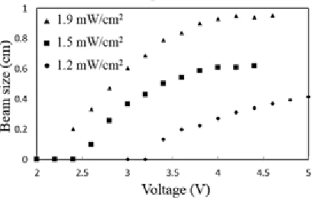
Figure 5 displays the beam sizes measured under various applied voltages at different UV light intensities. The voltages are added at intervals of 0.2 V. The threshold voltages and slopes of the curves are influenced by UV light intensities. Specifically, the threshold voltage drops under a strong UV intensity, thereby neutralizing the impurity electrons further. Slopes steep as a result of increased efficiency to offset the built-in field. If the average UV light intensity is 1.2 mW/cm2, then the threshold voltage is ~3.4 V. Furthermore, the slope of beam size and applied voltage in this curve is gentle than the slopes of the other two curves. The beam sizes are almost-linear functions of the externally applied voltages if the average UV light intensity is sufficiently strong at 1.9 mW/cm2. At this intensity, the size of the area that reaches the critical intensity of 2 mW/cm2 increases, and the maximum size of the beam is larger than those of the beams under the other two conditions.
In conclusion, the authors propose an LC-based electro-optic modulation for shutter and iris diaphragms. The device can operate as an adjustable light beam/ring by rotating the polarizer to either parallel/cross type and by tuning the externally applied electro-optic combinations of UV light intensities and voltages. An adaptive micro-electronic modulation may be developed for use in contact lenses or cell-phone cameras. Researchers may also replace the conductive polymer of PVK to enhance mobility, sensitivity to UV light or to react directly to a visible light band for special purposes.
4. 光開關原件與節能智慧窗-2
(Electrically controllable smart window with grayscale based on polymer stabilized cholesteric texture films) The study reports a novel liquid crystal (LC) film that can be applied on the transmissive substrates or sticked on existing casement window to upgrade the shield. The shadow area and transmittance can be adjusted according to the condition of the outer sunshine. The window is energy saving for which maintains the transmittance after an once-off operation of pulse amplitude modulation (PAM) electric driving. Such a film can be applied in smart curtain, display frame edge and other transmissive electro-optical devices.
The CLC mixture consists of nematic liquid crystal (E7, Merck), left-hand chiral dopant (S811, Fusol materials), monomer (RM257, Sigma Aldrich) and photo-iniator (Irgacure184, Beam); the concentrations of the chemical compositions are 91.47 wt%, 7.36 wt%, 0.93 wt% and 0.24 wt%. Because the reflection band is not located in the visible band, the film of planar texture looks transparent where the background is able to be seen through with clarity at the sunshine. By the way, for the reason that additional polymer is doped in it to stabilize cholesteric texture, the film is called polymer stabilized cholesteric texture (, abbreviated as PSCT).
The dilute solution of the alignment films are spin coated on the substrates and baked in the oven. Then, the cell is fabricated by sandwiching the parallel rubbed substrates with 8 μm pearl powder spacers. Then the solution is filled in the cell and cured by UV light (0.09 mW/cm2) with external voltage of 50 V to develop vertical polymer branches. After curing, the CLCs present in planar texture. All of the process in fabricating a curtain are the same, besides an empty wedge cell is prepared by sandwiching 4 μm and 8 μm pearl powder spacers at each fringe. The size of the wedge sample is ~ 1 cm*1.5 cm.
Figure 1 shows the driving scheme to perform the phase transitions of the cholesteric textures in the PSCT. The driving electric field is a 1 KHz pulse amplitude modulation (PAM) voltage which include a resetting process and an addressing process. The resetting process is to avoid the transitions between focal conic textures or that with planar texture by setting the cholesteric texture into homeotropic texture to reduce the hysteresis effect. The addressing process controls the cholesteric texture to transit into planar texture, focal conic texture or meso-textures, since the addressing voltage controls the pitch of the helical structure and the stacking of multiple domains in the evolution process so as to transit into the stable textures. Both the addressing voltage (Vaddress) and duration time (tduration) determine the transition results that directly affect the scattering of the film. In other words, the transparency of the film in the end can be tuned by changing the addressing voltage (Vaddress) and duration time (tduration) to achieve the specific cholesteric textures.
The meso-texture can be regards as focal conic texture for which contains multiple domain structure and scatters incident light, too. Therefore, the transitions are simplified into HP transition (the homeotropic texture to planar texture) and HF transition (homeotropic texture to focal conic texture). The diagram schematic draws the transmittance transformations in PAM driving and after that. The phase transitions in a wedge cell in which the cell is thin at the bottom and thick at the top are labelled on it. Note, because the effective field is different, the phase transitions are not the same for the top and bottom for an addressing voltage. For example, if the addressing voltage (Vaddress) is 20 V, the effective fields are 5 V/μm and 2.5 V/μm for the bottom and the top regions, respectively. Thus, the cholesteric texture experienced the transition from homeotropic texture to high-scattering focal conic texture and then the evolution to low-scattering focal conic texture in the addressing process at the thick region. Instead, the cholesteric texture does not change away from homeotropic texture in addressing process but transits from homeotropic texture to planar texture after that at the thin region.
Figure 2 shows the microphotographs of the PSCT after addressing process. If the addressing field is low, the helical pitch of cholesteric liquid crystal is short. Most wounded CLCs have less contact interface with the surface substrate, the liquid crystal tend to be anchored by the polymer matrix and randomly distributed. The texture scatters much light and the transmittance is low, see Fig. 2(a). If the addressing field is increasing, the helical pitch of cholesteric liquid crystal is longer, more less-wounded directors of the liquid crystal molecules align parallel to the surface by the homogeneous alignment film. The textures scatter less light and the transmittances become higher, see Fig. 2(b) - Fig. 2(d). However, if the addressing field decreasing abruptly, most of the strong wounded liquid crystals align on the surface perfectly. The planar texture scatters little light and the transmittance is high, see Fig. 2(e). The transmittances ordering of actual measured values from high to low is homeotropic texture (~90%), planar texture (~80%) and focal conic texture (~3 - 55%). Because the PSCT consists some polymer that scatters light slightly, the transmittance of the film reduces. The transmittance of the planar texture can be improved by decreasing the polymer concentration to reduce its scattering. Figure 2(f) shows the microphotograph at the interface between the planar texture and the focal conic texture in wedge cell. The lower region of planar texture is perfect; the upper region that contains focal conic textures shows some strips of periodic texture of CLCs.
The anchoring force from the polymer matrix and the surface homogeneous alignment film affect the stability of cholesteric texture, transition time and transmittance. If the cell has strong homogeneous alignment layers, the focal conic texture is not stable. Instead, if the anchoring force from the polymer is too strong, the CLC keeps in the homeotropic texture after the reset voltage. Even most of the CLCs transit into planar texture, the structure of the planar texture is not perfect, the transmittance is low. Hence, to choose an optimum homogenous alignment films in the multi-stable PSCT that has a fast response time, high transmittance and stable focal conic texture is important. Five homogeneous alignment films are employed to find an optimum balance of them by studying the transmittance curves in the transition of homeotropic texture to planar texture.
Figure 3 shows the transmittance curves in the transition from homeotropic texture to planar texture. The transition is achieved by applying the resetting AC pulse (50V at 1KHz for 1 s). After resetting, the CLCs transit from homeotropic texture to planar texture. Nucleation process takes place in the H-P transition that induces strong scattering of incident light.[28] In the case of weak anchoring force, the sample needs a relative long transition time. The alignment film of PVA has weak anchoring force, the transition time is long, also lower final transmittance for its imperfect planar texture. Instead, the cell with stronger homogeneous anchoring force transits into planar texture faster and higher final transmittance. The anchoring forces and transition times of the other three homogeneous alignment films are intermediate between them. Hence, the alignment film with stronger homogeneous anchoring force than commercial product is required. The response time for the transition with our self-made polyimide is ~ 10 s.
Figure 4 shows the transmittances of the PSCT in the H-F transitions. The insets in Fig. 4(a) show the photographs of the film for reference their transmittance. The H-F transition is performed by pulse amplitude modulation (PAM) driving to achieve stable states of focal conic textures. The addressing voltage is increasing from 6.5 V to 8 V while the duration
time are 6 s, the transmittances of them rise from 5.8% to 48%, see Fig. 4(a). As mention in the previous section, the transmittance of the focal conic textures tuned by controlling the order of CLCs in addressing process. To increase the addressing voltages, thus, induces higher transmittance of the PSCT. In figure 4(b), the duration time is increasing from 2 s to 12 s while the addressing voltage are 7.5 V. Because the focal conic texture has enough time to evolve into lower scattering texture, the transmittances of them rising from 13% to 42%. Note, the duration time in the resetting processing is ~ 1.5 s that affects little to the resulting transmittances if it is extended to a few seconds.
3.3 Performance of the blind window
The blind window is perform using PAM driving in the wedge cell. Table 1 demonstrates the results after PAM driving. The window that divided into five areas can be tuned from total block to total transparent by increasing the addressing voltage, see the first row. Because higher addressing voltage makes larger area keeps in homeotropic texture in the process, the area that transits into planar texture becomes larger from the bottom to the top. If the duration time is extended, the transparency of the opaque region can be tuned, see the second row. Because the duration time of addressing increases from 2 s to 15 s, the evolution time increases, the CLCs transit into low scattering focal conic texture (T~50%). Therefore, the opening of the window is adjustable and the transmittance of the opaque region can be tuned.
4 conclusion
In conclusion, an energy-saving blind window is demonstrated by PSCT on glass substrate. The author do not list a table of transmittance versus addressing voltage (or duration time), since there exist a range to reach the same transmittance of final stable focal conic textures. For example, the result transmittance of the combination of 7 V addressing voltage and 6 s duration time and that of 7.5 V addressing voltage and 2 s duration time are close. Despite, the 3% minimum transmittance and the tens second evolution time for lower scattering focal conic texture are not perfect, they can be improved by changing the cell gap variation and increasing the addressing voltage. The final purpose is to transplant to the film on the plastic substrate on the scale of a few feet square.
4.光開關原件與節能智慧窗-3
(Advanced electro-optical smart window based on PSLC using a photoconductive TiOPc electrode)
This study demonstrates an electro-optical controllable smart window based on a liquid crystal device. The device integrates a photoconductive electrode based on TiOPc films into a liquid crystal shutter based on polymer-stabilized homeotropic aligned nematic liquid crystals (PSLC) connecting in series. The PSLC light shutter is transparent in electric field-off state; it scatters light as it is switches to multi-domain structures in electric field-on states. The TiOPc film has an optically controllable impedance that manipulates the electric field on the PSLC film. The window transits into multi-transmission states according to the intensities of exposure light with an extra applied bias voltage.
Figure 1.
Working principle of the electro-optical light shutter for window. (a) Normally white mode as the electro-optical control is off, (b) scattering modes upon variable illuminated ambient light intensities, (c) schematic illustration of the photoconductive electrode, (d) photographs of the film captured from front-, back- side.The photosensitive window makes up of two components, including the photoconductive electrode of TiOPc film and the polymer stabilized liquid crystal film (PSLC). The impedance of the TiOPc film is a function of the exposure light written as ZTiOPc (I). In the circuit, the PSLC film and the electrode is in series connection.
Thus, the effective electric field on the PSLC film can be written as
(1)
The mechanism to tune the transmittance of the PSLC film via extra applied voltage is explained as follow. The initial state
PSLC TiOPc PSLC eff LC Z I Z Z V + ) ( , α
of the LC directors are in homeotropic alignment (or vertical alignment, VA) with polymer branches interspersed in it, see Fig. 1(a). The incident light passes through it without scattering. If the extra applied voltage is above the threshold, the LC directors tilt away from the field direction for its negative dielectric anisotropy. The PSLC film is switched to a multi-domain structure; light is scattered when passing through it, see Fig. 1(b). It is worth to mention that the LC film operates in normally white mode (reverse mode light shutter); it is transparent in the field-off state and opaque in the field-on state. Therefore, the electro-optical light shutter affords an advanced window that can automatically shield the sunlight. In addition, the window is green and safe, since it is transparent at zero field (or under interruption of power supply).
Figure 1(c) shows the schematic illustration of the stacking to compose the photoconductive electrode. The composite electrode is designed to conduct electricity better. The intermediate layers of PEDOT:PSS and silver glue are applied to improve contact flatness and stability. The terminal of cooper foil tape protects the silver glue avoiding the direct contact with the clamp. Figure 1(d) shows the photographs of the substrate with photoconductive electrode captured from front-, back- side. The size of the TiOPc film is ~ 10 mm* 20 mm. The impedance is inversely proportional to the area of the TiOPc electrode that can be adjusted in practical application.
Figure 2. Impedance versus frequency curves of TiOPc and PSLC film. In measuring the curves of the TiOPc film, an exposing tungsten halogen lamp is switched off/on, respectively. The inset shows the absorption spectrum of the TiOPc film.
TiOPc is a metal complexes of phthalocyanine compound. TiOPc compositions strongly absorbs light between 600 and 700 nm, thus the powders are blue to very dark blue. It has very low solubility in organic solvents resulting from the aromatic macrocyclic compound of phthalocyanine (s < 100 mg/mL). The formula of the TiOPc used in the study is C32H16N8OTi, see the inset of Fig. 2 whose formula weight is 576.39 g/mol. The core of the window is the production of TiOPc film from
granular powder. It is known that phthalocyanines have its polymorphism depending on the different conditions of the fabrication. Several commercial solvents are employed to dissolve the TiOPc powers. The polymer stabilized homeotropic aligned nematic liquid crystal film is fabricated as follow. The employed negative dielectric liquid crystal is HNG30400-200 (Fusol Material; 𝑛𝑛e = 1.633, 𝑛𝑛o = 1.484, ∆ε = -8.3). The monomer (2 wt%, RM257, Merk) and photo-initiator (0.2 wt%, Irgacure 651, Ciba Specialty Chemicals) are dissolved into the liquid crystal (97.8 wt%). Then, the solution is filled into an empty cell sandwiching with 20 μm pearl powder spacers; the surface of the cell are coated with DMOAP for vertical
alignment of the LCs. Finally, the film is exposed to an UV light (10 mW/cm2) for photo-polymerization; the curing requires 20 minutes for twice exposures from each side. The resulting polymer network is perpendicular to the cell surface that can homeotropic align nematic liquid crystals.
The inset of Figure 2 shows the absorption spectrum of the fabricated TiOPc film. The primary absorption bands of the coated TiOPc film locate at opposite ends of the visible spectrum (λ<430 nm; λ>660 nm). At the band of 450 nm- 610 nm, its absorption is less than 50%.The absorption band of the TiOPc makes the window suitable to detect the UV light or near infrared light but not sensitive to the green light. Figure 3 shows the impedance versus frequency curves of TiOPc film and PSLC film. Because the impedance of the photoconductive film of TiOPc depends on the mobility of the charge carrier, the curves are used to match the impedance of TiOPc film and PSLC film in driving. A tungsten halogen lamp is used to test the working range of the variable impedance under light illumination. The working range of the variable impedance is labelled by red-dash-line in which the light illuminance is 30 Lux. The impedance of the coated TiOPc film against certain light wavelength or light intensity is not study in detail, since the impedance change is on the same scale in daily life application. In the afterward, the frequency of the applied AC voltage in the demonstration is 100Hz.
Figure 3.Experimental setup used to measure the electro-optical switching of the film.
In the experiment, a He-Ne laser is used to measure the transmittance while the TiOPc electrode is exposed to a light source with an extra applied AC voltage (f=100 Hz). Because the TiOPc film has two absorption bands, He-Ne laser and UV light are used in the experiment.
Figure 4. Transmittance versus applied voltage curves of the PSLC window with its TiOPc electrode exposing to (a) He-Ne laser and (b) UV light with various light intensities.
Figure4 shows the transmittance versus applied voltage curves of the PSLC window with its TiOPc electrode exposing to He-Ne laser or UV light. The transmittance curves are measured with respect to the two light sources under various light intensities. Before the exposure to the light, the impedance of the TiOPc film is relatively high, the threshold voltage to drive the window is above 30 V. If the light is on (even weak, I > 0.25 mW/cm2), the transmittance responses to the extra applied voltage. The transmittance can be tuned between 9 % and 90 %. The operating voltage of 10 V up to 25 V for the window can be applied as per user’s requirements of transmittance (or penetration reduction).
Figure 4(a) demonstrates the electro-optical control of the window with respect to the exposure of a He-Ne laser. The window is optically controlled under a certain bias voltage, called light control mode. For example, if the bias voltage is 18 V, the transmittance reduces from 68 %, 35 % to 21 % as the light intensity increases from 0.25 mW/cm2, 1.5 mW/cm2 to 15 mW/cm2. Or, the window is electrically controlled under specific light intensity, call voltage control mode. For example, if the light intensity equals 0.25 mW/cm2, the transmittance reduces from 58 %, 35 % to 24 % as the applied voltage increases from 16 V, 18 Vto 20 V. The same electro-optical operation can be repeated under the exposure of the UV light, see Figure 4(b). The transmittance of the window is reduced from 53 %, 39 % to 26%, by increases the UV light intensity from 0.25 mW/cm2, 1 mW/cm2 to 5 mW/cm2 (biased at 18 V) or the applied voltage increases from 16 V, 18 V to 20 V (exposed to
0.25 mW/cm2).
Indoor and outdoor demonstration of the PSLC window
Figure 5. Photographs of the PSLC window switched to various transmittance for reference. (a) - (d) Indoor demonstration, the TiOPc electrode is exposed to He-Ne laser with various light intensities. (e) - (g) Outdoor demonstration, the solar irradiation (I ~ 3 mW/cm2, for λ=365 nm) from the sunlight is switched from off, half-on to on by a cover plate. The
left-bottom inset shows the transmittance for reference.
Figure 5 shows the photographs of the PSLC window switched to various transmittance for reference. The window is demonstrated indoor and outdoor, respectively. In Fig. 5(a) - Fig. 5(d), the intensity of the He-Ne laser equals 15 mW/cm2, the applied voltage increases from 8 V, 12 V, 16 V to 20 V, the corresponding curve is plotted in Fig. 5(a). At the outdoor demonstration of Fig. 5(e) - Fig. 5(g), the exposure of the solar irradiation (I ~ 3 mW/cm2, for λ=365 nm) from the sunlight is switched from off, half-on to on by a cover plate. The transmittance is switched from 88 %, 40 % to 15 % under the applied voltage of 20 V, the corresponding curve is plotted in Fig. 4(b).
In conclusion, an electro-optical smart window is designed by the integration of photoconductive electrode on the liquid crystal shutter. The smart window can automatically tunes the transmittance by solar irradiation changes. The advanced liquid crystal window features fast response time, long-term stability and high reliability under light and voltage dual control modes. The fabrication parameters of the photo-sensitive electrode of TiOPc film is adjustable to satisfy the demand elasticity for its many products.