國 立 交 通 大 學
電機與控制工程研究所
碩 士 論 文
每秒一百億筆資料傳輸之新型樹狀序列器傳輸端
A Novel Tree-Type Serializer for 10Gbps Transmitter
研 究 生:陳冠宇
指導教授:蘇朝琴 教授
每秒一百億筆資料傳輸之新型樹狀序列器傳輸端
A Novel Tree-Type Serializer for 10Gbps Transmitter
研 究 生:陳冠宇 Student : Guan Yu Chen
指導教授:蘇朝琴 教授 Advisor : Chau Chin Su
國 立 交 通 大 學
電機與控制工程研究所
碩士論文
A Thesis
Submitted to Department of Electrical and Control Engineering College of Electrical Engineering and Computer Science
National Chiao Tung University in partial Fulfillment of the Requirements
for the Degree of Master
in
Electrical and Control Engineering September 2006
Hsinchu, Taiwan, Republic of China
中華民國九十五年九月
每秒一百億筆資料傳輸之新型樹狀序列器傳輸端
研究生 : 陳冠宇 指導教授 : 蘇朝琴 教授
國立交通大學電機與控制工程研究所
摘 要
本論文提出一個可用在每秒一百億位元傳輸的序列輸出入端的新型樹狀序列器,利用 九十度相位差異的時脈來作為類似開關控制,以排除一般設計中對於時序再重置方法的需 要,因此在功率消耗與電路面積上能有顯著降低。模擬結果顯示在每秒一百億位元傳輸, 相較於一般的序列器,所推薦的序列器消耗百分之七十的功率以及百分之二十二的面積。 在本篇論文中,我們設計了一個每秒一百億位元傳輸器。使用台積電 0.13μ m 2P8M CMOS 製程來實現,此傳輸電路在 1.2 伏特的電源供應下消耗功率 27 毫瓦。 另外,我們也提出在晶片內部傳輸的通道模型以及所對應一公分通道長的低功率驅動 器設計。 關鍵字: 序列器, 多工器, 解序列器, 解多工器, 高速序列連結, 新型樹狀序列器, 九十度相位差異的時脈A Novel Tree-Type Serializer for 10Gbps Transmitter
Student: Guan Yu Chen Advisor: Chau Chin Su
Department of Electrical and Control Engineering
National Chiao Tung University
Abstract
This thesis proposes a novel tree-type serializer for 10Gbps serial I/O. It uses quadrature clocks as switch controls to eliminate the need for retiming in a conventional design. As a result, power consumption and circuit area is significantly reduced. Simulation results show that at 10Gbps the proposed serializer consumes 0.7 of power and occupies 0.22 of area as compared to a conventional one.
In this thesis, a 10 Gbps transmitter has been designed. It is implemented in TSMC 0.13μ m 2P8M CMOS process., the transmitter circuit consumes 27mW on a 1.2V power supply.
Besides, we analyze the on-chip channel model and design a low power driver for the 1cm channel.
Keyword: Serializer, Multiplexer, Deserialize, DeMultiplexer, High-speed serial links, novel tree-type serializer, quadrature clocks
致 謝
我首先要感謝我的指導教授 蘇朝琴老師,感謝老師指導我的研究以及做研究的精神。
接著要感謝大師兄 鴻文學長,您總是很有耐心的指點學弟;還要感謝丸子學長,在您 的維持下,實驗室才能正常運作,打 AOC 才不會 lag,嗯…,我是說 Layout 才不會 lag; 當然還要謝謝仁乾和盈杰學長的指教和建議。 還要謝謝王照勳學長,感謝您在 TSMC0.13um 製程上不厭其煩的解答。還有汝敏在 TSMC0.13um 製程上的鼎力相助和洪老師實驗室的鼎鈞與振綱與我討論製程的問題以及 CIC 的 TSMC0.13 負責人張文旭先生解答任何我在製程上的使用問題,感謝你們。當然不能忘記 中央的各位學長們,包括顯元學長,毅山學長,育凱學長幫我下探針,常常陪我一忙就是 一整天,真是讓我萬分感激也十分不好意思,謝謝你們。另外還要謝謝煜輝學長,阿亮學 長,阿達學長,瑛佑學長,Cgu 學長,Ku 學長,阿銘學長的指導,還有志龍跟大姐與我分 享量測上的經驗,以及忠傑,順閔,TOTORO,小朱的幫忙。 再來要感謝智琦無私的解答,以及招牌般的笑容,恭喜老大你脫團了(哼)~~~,果然 好心有好報。還有匡良,楙軒,宗諭,大家彼此之間的鼓勵打氣與互相扶持。還有祥哥, 教主,皇如,村鑫,小馬,奶油哥,方董,威翔,存遠,大家一起烤肉打球聊天的時光是 美好的回憶。 當然,還有助理依萍,雅雯,俊秀,感謝妳們通知我們新消息以及…嗯,開會通知和 簽到表(Bad Dream~~)。 還要感謝士豪,教練,螞蟻,小 z,還有大學同學們的鼓勵,謝謝大家 最後當然是要感謝我的家人-爸爸,媽媽,沒有您們的鼓勵和支持,也不會有今天的我, 感謝你們。 陳冠宇 2006/7/23
List of Contents
List of Contents
List of Contents ...V
List of Tables... VI
List of Figures...VII
Chapter 1 Introduction...1
1.1CMOSHIGH-SPEED SERIAL LINKS 1
1.2MOTIVATION 3
1.3THESIS ORGANIZATION 4
Chapter 2 Background Study ...5
2.1OTHER STRUCTURE OF SERIALIZER 5
2.2SHIFT-REGISTER TYPE SERIALIZER 8
2.3SINGLE-STAGE TYPE SERIALIZER 9
2.4CONVENTIONAL TREE-TYPE SERIALIZER 10
Chapter 3 The Novel Tree-Type Serializer ...12
3.1FUNCTIONAL BLOCKS 12
3.2COMPARISON OF THREE STRUCTURES 15
3.2.1 ANALYSIS OF NOVEL TREE-TYPE AND SINGLE-STAGE SERIALIZER 16
3.2.2 COMPARE THREE ARCHITECTURES BY HSPICE SIMULATION 20
3.2.2.1 SINGLE-STAGE SERIALIZER 21
3.2.2.2 NOVEL TREE-TYPE SERIALIZER 24
3.2.2.3 CONVENTIONAL TREE-TYPE SERIALIZER 27
3.2.3 THE COMPARISON RESULTS AS FIGURES AND TABLES 31
3.3SUMMARY 37
Chapter 4 Transmitter Circuit Design ...38
4.1INTRODUCTION 38 4.2CIRCUIT DESIGN 38 4.2.1 MUX 8-TO-1 39 4.2.2 MUX 4-TO-1 42 4.2.3 MUX 32-TO-1 44 4.2.4 DRIVER 45 4.3SIMULATION RESULT 45 4.4IMPLEMENTATIONS 48
List of Contents
4.5SUMMARY 52
Chapter 5 Measurement...53
5.1OFF CHIP 53
5.2ON WAFER 56
Chapter 6 On-Chip channel model analysis and low power driver.. 59
6.1 On-Chip Channel Model Analysis 59
6.2 Low Power Driver 62
Chapter 7 Conclusion ...65
7.1 CONCLUSION 65
List of Tables
List of Tables
Table 1.1 High-Speed Communication Standard 3
Table 2.1 Comparison of three kinds of MUX 11
Table 3.1 Rise Time versus size of the MOS Transistors in Single-Stage Serializer 23 Table 3.2 Rise Time versus size of the MOS Transistors in Novel Tree-Type Serializer 26
Table 3.3 Rise Time versus size of the MOS Transistors in Conventional Tree-Type Serializer 29
Table 3.4 Power of three architectures versus Rising Time 32
Table 3.5 Area of three architectures versus Rising Time 32
Table 3.6 Power X Area of three architectures versus Rising Time 34
Table 3.7 Analysis vs. Simulation 36
Table 3.8 Power and Area Comparisons 37
Table 3.9 Power and Area Comparisons Standardizes by Using Conventional Tree 37 Table 4.1 The Power Consumption of Each Part of Circuit 47
Table 5.1 Measurement result 58
Table 6.1 Characteristic Impedance of M8-MY 62
List of Figures
List of Figures
Figure 1.1 Conventional Transceiver 2
Figure 2.1 Diagram of N-to-1 multiplexer 6
Figure 2.2 Shift-register type serializer 6
Figure 2.3 Single-stage type serializer 7
Figure 2.4 Conventional tree-type serializer 7
Figure 2.5 Serializer of CML 8
Figure 2.6 Circuit of 4-to-1Single-Stage Type 9
Figure 2.7 Circuit of 2-to-1 MUX in tree-type serializer 11
Figure 3.1 The original and proposed tree-type multiplexers 13
Figure 3.2 4-to-1 Novel Tree-Type Serializer 14
Figure 3.3 8-to-1 Novel Tree-Type Serializer 14
Figure 3.4 Timing Diagram of The Proposed MUX 15
Figure 3.5 Architecture of The Novel Tree-Type Serializer with2 to 1 N 15
Figure 3.6 8-to-1 Single-Stage Serializer 16
Figure 3.7 Basic Inverter 16
Figure 3.8 Half Circuit of Single-Stage and Novel Tree-Type Serializer 17
Figure 3.9 Equivalent R,C Circuit of Serializer 17
Figure 3.10 Static DFF 21
Figure 3.11 DFF of Clock Generator 21
Figure 3.12 Design steps for single-stage serializer 22
Figure 3.13 Eye Diagram of Rise Time of 300ps for Single-Stage Serializer 23
Figure 3.14 Eye Diagram of Rise Time of 150ps for Single-Stage Serializer 24
Figure 3.15 Steps of Simulation of Novel Tree-Type Serializer 25
Figure 3.16 Eye Diagram of Rise Time of 300ps for Novel Tree-Type Serializer 26
Figure 3.17 Eye Diagram of Rise Time of 100ps for Novel Tree-Type Serializer 27
Figure 3.18 8-to-1 conventional tree-type architecture 28
Figure 3.19 Eye Diagram of Rise Time of 300ps for Conventional Tree-Type Serializer 29
Figure 3.20 Eye Diagram of Rise Time of 100ps for Conventional Tree-Type Serializer
30
Figure 3.21 Area v.s. Rising Time 31
Figure 3.22 Power v.s. Rising Time 33
Figure 3.23 Area v.s. Rising Time 33
List of Figures
Figure 3.25 Power X Area v.s. Rising Time of Two Structures 35
Figure 3.26 Analysis vs. Simulation 36
Figure 4.1 Whole Architecture of the Chip 39
Figure 4.2 Clock Diagram of 8-to-1 MUX with Propagation Delay 39
Figure 4.3 Proposed Novel Tree-Type Serializer 40
Figure 4.4 Circuit of Differential DFF 40
Figure 4.5 Structure of 8-to-1 MUX and Clock Gen 41
Figure 4.6 Data and Clock Diagram of 8-to-1 MUX with Delay 42
Figure 4.7 (a) CS Circuit with Load C (b) Small Signal Equivalent Circuit of (a) (c) CS Circuit with additional inductor (d) Small Signal Equivalent Circuit of (c) 43
Figure 4.8 Circuit of 4-to-1 MUX 43
Figure 4.9 Data and Clock Diagram of 4-to-1 MUX with Delay 44
Figure 4.10 Architecture of 32-to-1 MUX 44
Figure 4.11 Architecture of Multi-Stage Driver 45
Figure 4.12 Simulation Result of The Multi-Phase Generator
46
Figure 4.13 Simulation Result of 8-to-1 Serializer 46
Figure 4.14 Simulation Result of 4-to-1 Serializer 47
Figure 4.15 The Eye Diagram of 10Gbps Transmitter 47
Figure 4.16 The Effect of Ground Bounce to VDD and GND 48
Figure 4.17 Layout of MUX2 and DFF 48
Figure 4.18 Retiming and PRBS DFF 49
Figure 4.19 8-to-1 MUX 49
Figure 4.20 (a) Clock Generator for 8-to-1 MUZ (b) 4-to-1 MUX (c) 5GHZ to four phase 2.5GHZ Clock divider 49
Figure 4.21 32-to-1 Serializer 50
Figure 4.22 Layout of Whole Chip (Without Dummy) 50
Figure 4.23 Layout of Whole Chip (With Dummy) 51
Figure 4.24 The Whole Measurement Environment 52
Figure 5.1 The Whole Chip Photo 54
Figure 5.2 The Core Photo 54
Figure 5.3 Structure of Four layers PCB 54
Figure 5.4 Photo of Off-Chip Measurement PCB 55
Figure 5.5 Environment of Off-Chip Measurement 55
Figure 5.6 (a) 1.25Gbps Data Eye Diagram (b) Reset 55
Figure 5.7 2.5Gbps Data Eye Diagram 56
Figure 5.8 Wenworth probe station 57
List of Figures
Figure 5.10 Probe Photo 57
Figure 5.11 (a) Eye Diagram 1 (b) Eye Diagram 2 58
Figure 6.1 (a) Microstrip (b) Stripline 60
Figure 6.2 On-Chip Channel Model Design Flow 61
Figure 6.3 (a) Structure of Driver (b) Impedance matching 63
Figure 6.4 Architecture of Pre-Driver 64
Chapter 1 Introduction
Chapter 1
Introduction
1.1 CMOS High-Speed Serial Links
High-speed serial links in Gbps range are usually implemented in bipolar or GaAs technologies. The primary reason is the higher bandwidth of those devices. However, CMOS transistors process technology has grown exponentially in recent years. It results in a remarkable improvement in the operating speed and integration level. [1]
Figure 1.1 is a conventional serial link system. It comprises three primary components: a transmitter, a channel, and a receiver. The high-speed data sent by a transmitter are analog signal. These analog signals known as non-return-to-zero (NRZ) use either a HIGH-level or a LOW-level to represent data bits. For an optical transmission system, these levels are different amounts of optical power. For electrical systems, these levels are different signal voltage or current pulses.
Chapter 1 Introduction
parallel bits into a serial bit stream. The timing information is embedded in this serial data. The output drivers drive the signal from serializer to the channel.
The channel is the medium of the data transmission system. There are many types of channels, such as unshielded twisted-pairs, printed-circuit boards (PCB) transmission lines, chip packages, coaxial cables and optical fibers. There are two high-speed links, copper cables and optical fibers. The first one as for short distance transmission and the second as for long distance ones. The most significant advantage provided by optical fibers is high bandwidth over long distances. But the drawback is the cost since the optical fiber and the necessary components as expensive. To replace optical fiber, the less expensive solution for high-speed communication is using cooper cables. But the cable length limits the bandwidth of transmission.[2]
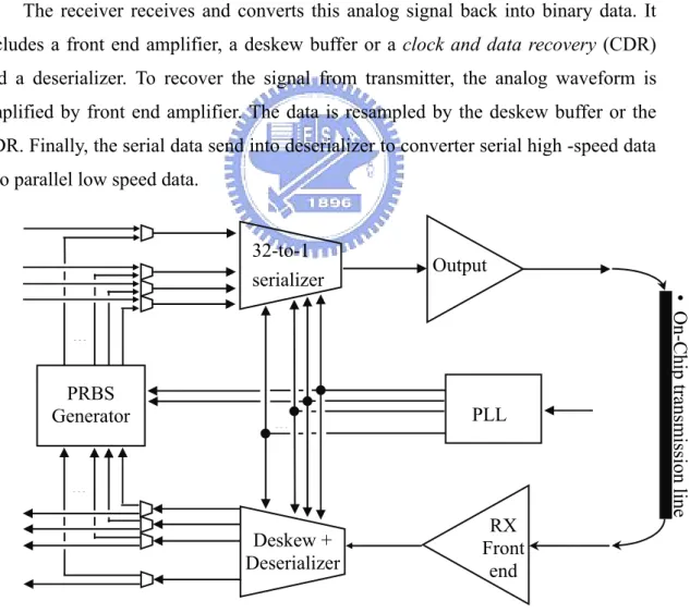
The receiver receives and converts this analog signal back into binary data. It includes a front end amplifier, a deskew buffer or a clock and data recovery (CDR) and a deserializer. To recover the signal from transmitter, the analog waveform is amplified by front end amplifier. The data is resampled by the deskew buffer or the CDR. Finally, the serial data send into deserializer to converter serial high -speed data into parallel low speed data.
Figure 1.1 Conventional transceiver
In advanced design case, there is a Pseudo Random Bit Sequence (PRBS) generator and verifier. The function is to check the correction of the data received
PLL Output RX Front end PRBS Generator Deskew + Deserializer … … … • On-Chip transmission line 32-to-1 serializer
Chapter 1 Introduction
from receiver by comparing to the data in transmitter. This is a build in self test (BIST) system. Phase lock loop (PLL) provides both transmitter and receiver a clock source. The CMOS high-speed serial links have been widely used in many applications such as data transmission with multiple processors, communication within computers, routers, etc. Also, there are many standard specification for CMOS high-speed serial links, like Gigabit Ethernet, IEEE1394, SONET, Fiber Channel. Table 1.1 is the table of standards
Table 1.1 High-Speed Communication Standard
Standard Data Rate
OC-12/STM-4 622.08Mbps FC1063 1.0625Gbps SATA 1.5Gbps OC-48/STM-16 2.48832Gbps PCI-Express 2.5Gbps SATA2 3Gbps XAUI 3.125Gbps 4G FC 4.25Gbps 8G FC 8.5Gbps OC-192 9.95328Gbps 10GbE 10.3125Gbps Fiber Channel 10.51875Gbps G.709 10.66423Gbps G.975 10.70923Gbps OC-768 39.81gbps
1.2 Motivation
Advanced integrated circuit technologies are able to integrate muilti-million gates into a single chip. Operating frequency and data throughput have been increased significantly. Conventionaly, parallel buses and serial links are two approaches for high-speed signaling. For parallel buses, many bus lines are needed in a system to make the total transmission data rate arrive the specification. The drawback of the large buses is the increased power consumption and the explosion of circuit area. Also, the pads numbers is increased. Unfortunately, the number of I/O pins cannot grow proportionally. As a result, high-speed serial I/O is needed to solve the communication
Chapter 1 Introduction
bottleneck. PCI-Express and Serial ATA are two prominent examples. For serial transmission links, it maximizes the communication bandwidth and distance in a single transmission line. Serial links offer a high-speed and low-cost solution to multi-gigabit per second rates over long distance. Applications such as computer-to-computer or computer-to-peripheral interconnection can reach several meters. A key component is a serialier that converts low-speed parallel data into high-speed serial output stream.
In this thesis, a novel tree-type serializer circuit is proposed. We implement this transmitter architecture using non-return-to-zero (NRZ) signal techniques. A 10 Gbps novel tree-type serializer with output driver and PRBS (Pseudo Random Bit Sequence) has been designed. We also analyze the on-chip channel mode and design a low power driver for the channel with 1cm length.
1.3 Thesis organization
The rest of the paper is organized as follows.
In Chapter 2, we describe and analyze the conventional structure of serializer. In Chapter 3, we introduce the proposed novel tree-type serializer architecture and analyze and compare to other conventional architecture. The simulation results of comparation are also showed.
In Chapter 4, the chip implementation is presented. We show the full architecture of this transmitter. We also show the detail circuit of each block. Finally, we present the simulation results, layout, and measurement consideration of the design.
In Chapter5, the measurement results are presented. It includes off-chip measurement and on-wafer measurement by a probe station. The results include eye diagrams, jitters (Pk-Pk)(RMS), power consumptions.
In Chapter 6, we show an on-chip channel model analysis and a low power driver.
Chapter 2 Background Study
Chapter 2
Background Study
2.1 Other Structure of Serializer
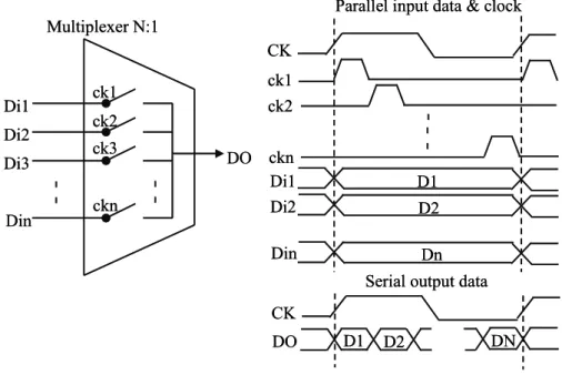
Serializer, also called Multiplexer or MUX, has the function of converting parallel low speed input data into serially high-speed output data stream. As Figure 2.1 shows, a conceptual block diagram of a serializer. In Figure 2.1, there is a N-to-1 multiplexer. Di1 to Din are n-bit parallel low speed input data. Selected by ck1 to
n
ck , Di1, Di2 and Din are serialized into high-speed output, DO. Its data rate is n times of Di. In many applications, the number of inputs of serializer is power of two, like 2, 4, 8, 16. Some system like PCI-Express may encode the output data. Thus, the number of input of serializer may be changed to another number. For example as 8B/10B scrambler need a 10 to 1 multiplexer.
There are three principal structures of serializer. They are shift-register type, single-stage type, and tree-type serializer. The architecture is shown in Figure 2.2, 2.3, and 2.4. There are other special architectures, like CML (Current Mode Logic) MUX
Chapter 2 Background Study
as shown in Figure 2.5. We will explain the structures in the next chapter.
ck1 ck2 ck3 ckn DO Multiplexer N:1 Di1 Di2 Di3 Din CK ck1 ck2 ckn Di1 Di2 Din D1 D2 Dn
Parallel input data & clock
Serial output data CK DO D1 D2 DN ck1 ck2 ck3 ckn DO Multiplexer N:1 Di1 Di2 Di3 Din CK ck1 ck2 ckn Di1 Di2 Din D1 D2 Dn
Parallel input data & clock
Serial output data CK
DO D1 D2 DN
Figure 2.1 Diagram of N-to-1 multiplexer
Figure 2.2 Shift-register type serializer CK1 CK3 CK2 D D0 D3 D2 D5 D4 D7 D6 D1 out CK1 CK2 CK3 Out D7 D0 D1 D2 D3 D4 D5 D6 D7 0 D
Chapter 2 Background Study Φ1 Φ2 Φ3 Φ0b Φ1b Φ2b Φ3b d0 d1 d2 d3 d4 d5 d6 d7 Out Φ0 Φ0 Φ1b d0 Φ1 Φ2b d1 Φ2 Φ3b d2 Φ3 Φ0 d3 Φ0b Φ1 d4 Φ1b Φ2 d5 Φ2b Φ3 d6 Φ3b Φ0b d7 Outb Φ0 Φ1b d0b Φ1Φ 2b d1b Φ2Φ 3b d2b Φ3 Φ0 d3b Φ0b Φ1 d4b Φ1b Φ 2 d5b Φ2b Φ3 d6b Φ3b Φ0b d7b Out Φ1 Φ2 Φ3 Φ0b Φ1b Φ2b Φ3b Φ1 Φ2 Φ3 Φ0b Φ1b Φ2b Φ3b d0 d1 d2 d3 d4 d5 d6 d7 Out Φ0 Φ0 Φ1b d0 Φ1 Φ2b d1 Φ2 Φ3b d2 Φ3 Φ0 d3 Φ0b Φ1 d4 Φ1b Φ2 d5 Φ2b Φ3 d6 Φ3b Φ0b d7 Outb Φ0 Φ1b d0b Φ1Φ 2b d1b Φ2Φ 3b d2b Φ3 Φ0 d3b Φ0b Φ1 d4b Φ1b Φ 2 d5b Φ2b Φ3 d6b Φ3b Φ0b d7b Out
Figure 2.3 Single-stage type serializer
Figure 2.4 Conventional tree-type serializer /2 /2 CK/2(0°) D D D Ou 1 2 3 4 D0 D1 L L CK/2(90°) CK CK/2 (90°) CK CK/2 (0°) Out 1 2 3 4 1 2 3 4 D1 D0 D1 D0
2 to 1 MUX cell timing diagram
D0 D1 D2 D3 D4 D5 D6 D7
Mux Mux Mux
Mux Mux Mux Mux Latch D Flip Flop 2 to 1 MUX cell
Chapter 2 Background Study d1 d1b d2 d2b S SN Vb d1 d1b d2 d2b S SN Vb Figure 2.5 Serializer of CML
2.2 Shift-Register Type Serializer
Figure 2.2 shows the shift-register type serializer. The main function of this architecture is parallel load and serial shift. Both work of different frequencies. Parallel load works of low data rate. It uses CK2 as the clock. The parallel data inputs load in the D Flip Flop (DFF). Serial shift works of high-speed data rate It uses CK1 as function clock. The high data rate DFF trigged by CK1 sends data into a sequenced stream. The data in the serial shift register have been sent out entirely. CK3 loads the data from parallel load register into serial shift register. CK1 has the highest clock rate. It is divided to produce CK2, CK3. Refer to the timing diagram of the clock and data in Figure 2.2, this serializer works as follows.
The shift-register type serializer is a straightforward implementation. It can process arbitrary number of parallel data by increasing the number of DFFs and adjusting clock rate. The jitter is small with an ideal clock. However, there are several drawbacks. First, the maximum operating speed of this circuit is limited by the device performance. [3]. According to [4], only 3gbps transmission can be achieved even with 0.15um CMOS transistors technology. Second, it needs an extreme high speed and low jitter global clock. The DFF of serial shift work at the highest rate. This causes a large power consumption.
Chapter 2 Background Study
2.3 Single-Stage Type Serializer
Figure 2.6 Circuit of 4-to-1Single-Stage Type
Figure 2.3 is the structure of a single-stage type serializer. Figure2.6 is the basic circuit diagram of this structure. The multiplexer needs to input the clock with the same frequency as the parallel input data. As show in Figure 2.3, the data is sent out when two specific clocks with different phases overlap. For example, d0 is transmitted when Φ0 and Φ1b overlap (both are 1). The data period of d0 is from Φ0 positive edge to Φ1b negative edge. The other data are transmitted by the same rule.
There is also one point that should be remarked in Figure 2.6. Many papers show that the device of data input is just a NMOS transistors.[5~10]. But, in [11] [12], we know that adding an extra PMOS transistors of data input has a benefit. When data is low, the PMOS transistors turns on and drives current to precharge the internal node to a high level. In other words, this technique can reduce the charge sharing effect and alleviates data jitter.
In order to have large output swing, the pull-up PMOS transistors must be weakly sized to reduce the driving capability. This makes the low to high transient time larger and the unbalance of rising and falling times. To achieve higher speed, we should reduce the output swing. The analyses of output swing and delay time to pull-up PMOS transistors size are shown in [10].
Basically, it is a multiplexer controlled by the phases of a multi-phase low-speed clock. The power consumption is small. This serializer can also handle arbitrary number of parallel data. It sends out one bit of data at each phase interval. The most significant drawback is the large self parasitic capacitance at the outputs that limit the bandwidth performance.[1][9] Furthermore, phase imbalance of the clock may also
O d1b d2b d3b d4b P2 P1 P1 P4 P4 P3 P3 P2 Ob d1 d2 d3 d4 P2 P1 P1 P4 P4 P3 P3 P2
Chapter 2 Background Study
create jitters.
2.4 Conventional Tree-Type Serializer
Figure 2.4 shows a 8-to-1 tree-type serializer for high-speed applications. It is composed of three stages of 2-to-1 multiplexers organized as a tree. A high-speed clock, normally at half the data rate, is divided to control the successive stages. However, due to the two inputs need to be out of phase, retiming mechanism is required [13~15]. We describe the 2-to-1 MUX in detail in Figure 2.4. We use CK/2(0) to retime DFF. D0 is latched by one positive triggered DFF. D1 is latched by one positive triggered DFF and one negative triggered DFF. After the retiming, D0 and D1 have a 180 degree phase shift. Then those two data as sent into a 2-to-1 MUX and we use CK/2(90) to select data out of the MUX. Notice the timing diagram of Figure 2.4, using CK/2(90) to select data during 1/4 to 3/4 the data period ensures enough setup time and hold time.
The conventional tree-type serializer is able to operate at a high frequency due to the low output parasitic capacitance and retiming mechanism. This architecture can only convert power of two of parallel input data, such as 2, 4, 8, and 16. It is able to achieve higher speed than a single-stage serializer. However, its hardware overhead and power consumption is higher.
Figure 2.5 and Figure 2.7 are the conventionally circuits of 2-to-1 MUX block. Figure 2.5 shows a CML of 2-to-1 MUX. It has a current source NMOS transistor biased by Vb to support a biasing current. The select S and inversion SN decide either d1 or d2 to be transmitted. As CMOS process technology scaled fast in recent years, supply voltage is lowed. The implementation of CML is harder due to three stages of NMOS transistors. Figure 2.7 is much alike a single-stage serializer and has lower parasitical capacitance at output node. Figure 2.7(a) is a 2-to-1 single-stage circuit and Figure 2.7(b) adds a PMOS transistor data input to reduce charge sharing effect as describe before.
Chapter 2 Background Study
Figure 2.7 Circuit of 2-to-1 MUX in tree-type serializer
Table 2.1 is a comparison of three types of MUX. The advantage is that this structure can work using a ring oscillator type phase lock loop (PLL). This means that the needed clock rate is 1/N of the transmission data rate.
Tree-type serializer is composed of multiple stages. This makes the number of input in each stage as well as the parasitical capacitance at output node be reduced. For this reason, the bandwidth of tree-type serializer is the highest among the three structures. The shortcoming is the requirement of a higher clock rate.
Table 2.1 Comparison of three kinds of MUX
High freq, single phase
Low freq, multi-phase High freq, single
phase External clock property medium Low High Bandwidth High Medium Low Power N N Multiplex number Shift-register Single-stage Tree
High freq, single Low freq,
multi-High freq, single External clock Bandwidth Medium N N Multiplex number Tree N 2 O d2 d1 CK CKB Ob d1b CK O d2 d1 CK Ob d1b d2b CKB CK (a) (b) CKB CKB d2b
Chapter 4 Transmitter Circuit Design
Chapter 3
The Novel Tree-Type Serializer
3.1 Functional Blocks
In this chapter, we will introduce a new serializer structure which consumes less power and area. First, we explain the 2-to-1 MUX and the control clock. Second, we show the configuration of 4-to-1 and 8-to-1 MUX. Finally, we describe the design issue. Figure 3.1 shows the conventional and proposed novel tree-type 4-to-1 serializer (multiplexer) cells. Three retiming D-type Flip-Flops (DFF), as shown in Figure 2.4, are removed. Instead, quadrature clocks are used for the switch control in the previous stage. The first stage is controlled by the original clock to switch and output data at two times the clock rate. The second stage is controlled by two divide-by-two clocks with phase difference of 90 degree. As one can see, with quadrature clocks, o
retiming can be waived. Moreover, data is ready one half period before being switched in. Therefore, there is no data dependent jitter. The overall jitter is determined by the output control clock.
Chapter 4 Transmitter Circuit Design
Figure 3.1 also shows the timing diagram without propagation delay. Therefore, there is no timing variation at the output. Figure 3.2 and Figure 3.3 are 4-to-1 and 8-to-1 MUX with quadrature clocks. The circuit structure is simple and regular. Without propagation delay, each stage of this serializer will have the setup time which is half of the input clock period and have no hold time.
The propagation delay is a design issue in chip implementation. Figure 3.4 shows the case that considers the propagation delay. T1 is the delay of clock divide; T2 is the delay of the MUX; T3 is one-bit time. As one can see, the setup timing margin is T3-T1-T2; and the hold time margin is T1+T2. In general, they are more than enough for the MUX to operate reliably.
Figure 3.1 The original and proposed tree-type multiplexers.
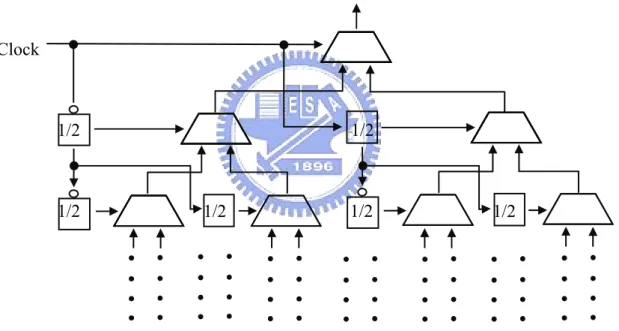
Figure 3.5 shows the architecture of the novel tree-type serializer with2 to 1. N
The circuit structure is simple and regular. The novel tree-type serializer embeds data retiming in the previous stage of MUX. Due to this, hardware overhead and power consumption are expected to be lower.
Modified mux cell & timing
Out I1 I0 I1 I0 I1 I0 CK/2 (90°) CK/2 (0°) CK D0 D1 D Q D Q D Q CK (0°) CK (90°) I1 I0 D1 I1 I0 I1 I0 D0
Original mux cell & timing
D1 D0 Out CK/2 (90°) CK (90°) CK (0°) Out D0 D1 D0 , D1 CK/2(0) CK CK/2(90) D0 D1 D0 D1 Out D1 D0 D1 D0 D1 D0
Chapter 4 Transmitter Circuit Design
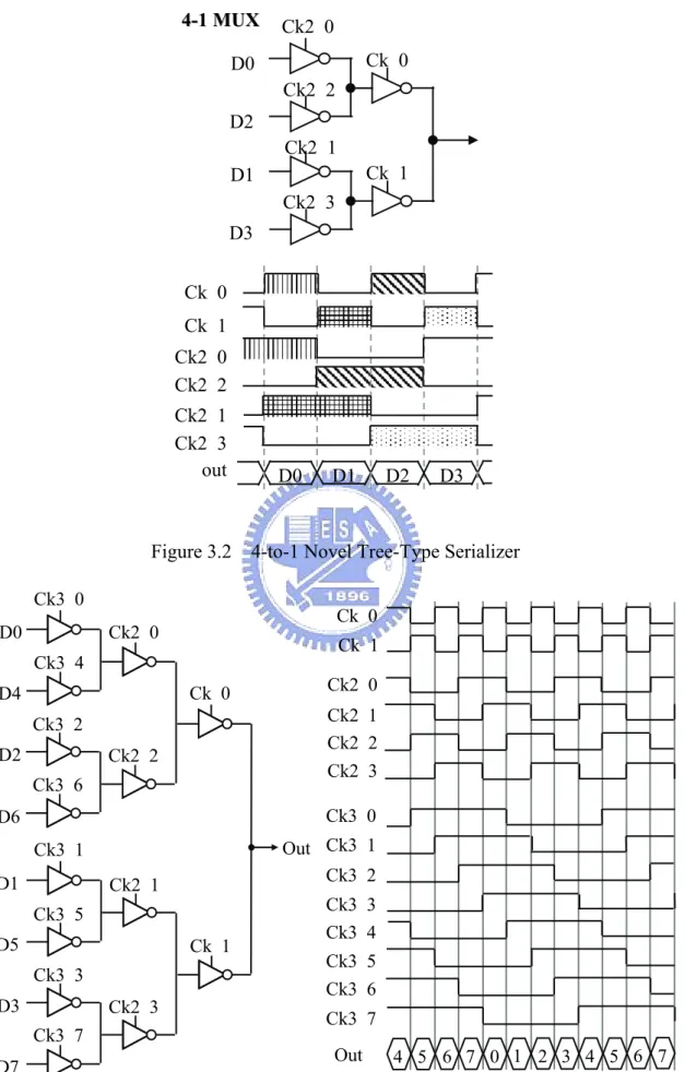
Figure 3.2 4-to-1 Novel Tree-Type Serializer
Figure 3.3 8-to-1 Novel Tree-Type Serializer Ck 0 Ck 1 Ck2 0 Ck2 2 Ck2 3 Ck2 1 D0 D1 D2 D3 out Ck 0 Ck2 0 Ck2 2 D0 D2 Ck 1 Ck2 3 Ck2 1 D1 D3 4 4--11MMUUXX Ck 0 Ck 1 Ck3 3 Ck2 1 Ck3 5 Ck2 2 Ck3 1 Ck2 3 Ck3 2 Ck2 0 Ck3 4 Ck3 0 Ck3 6 Ck3 7 Ck 0 Ck 1 Ck2 0 Ck2 2 Ck3 0 Ck3 4 Ck3 6 Ck2 3 Ck2 1 Ck3 1 Ck3 5 Ck3 7 Ck3 2 Ck3 3 D3 D2 D1 D0 D7 D6 D5 D4 Out 0 1 2 3 4 5 6 7 4 5 6 7 Out
Chapter 4 Transmitter Circuit Design
Figure 3.4 Timing Diagram of The Proposed MUX.
Figure 3.5 Architecture of The Novel Tree-Type Serializer with2 to 1. N
3.2 Comparison of Three Structures
We compare our novel tree-type serializer to the single-stage and the conventional tree-type serializer in this section. In section 3.2.1, we analyze the required number of PMOS transistors in single-stage and novel tree-type serializer. This could help we understand the speed limitation of them. We can also know the difference of size in the two architectures when both of them work in the same transient time and boundary conditions. Section 3.2.2, we compare the three
1/2 1/2 1/2 1/2 1/2 1/2 Out I1 I0 I1 I I1 I CK/2(90°) CK/2(0°) C D D I-Q Gen CK/2(0) CK CK/2(90) Out D1 D0 D0 D1 D0 D1 T1 T2 T2 Tsetup Thold T3 Clock
T1 : I-Q Gen delay, T2 : MUX delay, T3:half CK period Tsetup : Setup time timing margin = T3 – T1 – T2 Thold : hold time timing margin = T3 – Tsetup
Chapter 4 Transmitter Circuit Design
architectures by using HSPICE for simulation. The simulations of the three architectures are with the same boundary conditions to ensure the fair of comparison. Section 3.2.3, we show the comparison results as figures and tables.
3.2.1 Analysis of Novel Tree-Type and Single-Stage Serializer
Considering the chip design issue described in Chapter 4, we need four 2.5Gbps 8-to-1 serialzer and one 10Gbps 4-to-1 serializer. Therefore, the analysis and simulation focus on the 2.5Gbps 8-to-1 serializer. Figure 3.6 shows the 8-to-1 single-stage serializer with dummy PMOS transistor which alleviate the charge sharing effect.
Figure 3.6 8-to-1 Single-Stage Serializer.
We consider a basic inverter in TSMC 0.13μ technology. The design rule for m smallest width is 0.3μ . The basic inverter is shown in Figure 3.7. m
Figure 3.7 Basic Inverter.
The average of C and d C of PMOS transistor and NMOS transistor of the g inverter is as follows. Thus, 0.13um 1.3um ) L W ( p = 0.13um 0.3um ) L W ( N = fF 486 . 0 C fF 9294 . 1 C fF 747 . 0 C fF 5714 . 2 C NMOS PMOS avg _ gN avg _ gP avg _ dN avg _ dP = = = =
Chapter 4 Transmitter Circuit Design
( 1)
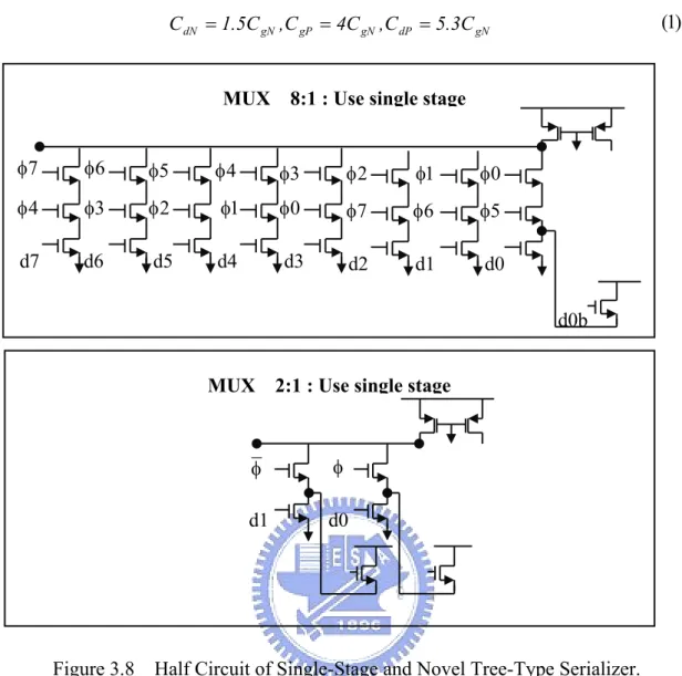
Figure 3.8 Half Circuit of Single-Stage and Novel Tree-Type Serializer. Figure 3.8 show the half circuit of these two architectures. Since three stage of 2–to-1 MUX compose a 8-to-1 novel tree-type serializer, we only need to show the last 2-to-1 MUX which dominates the output capacitance and bandwidth. The boundary conditions we assume are (1) for C , we consider PMOS transistor drain out capacitance and up level NMOS transistors drain capacitance. (2) the dummy transistor is not considered. (3) the swing in each architecture is from 0.25V to 1.2 V.
Figure 3.9 Equivalent R,C Circuit of Serializer.
MUX 8:1 : Use single stage
0 φ d0 d1 d2 d3 d4 d5 d6 d7 1 φ 2 φ 3 φ 4 φ 5 φ 6 φ 7 φ 0 φ 1 φ 2 φ 3 φ 4 φ 5 φ 7 φ 6 φ d0b
MUX 2:1 : Use single stage
d0 d1 φ φ RO_P RO N CO VDD VO e Capacitanc l Parasitica Output C NMOS of Resistance Output R PMOS of Resistance Output R O O_N O_P = = = gN dP gN gP gN dN 1.5C ,C 4C ,C 5.3C C = = =
Chapter 4 Transmitter Circuit Design
We calculate the delay time from the output resistance and capacitance of serializer. We use equivalent RC circuit shown in Figure 3.9 to simplify the calculation. The calculations is are
( 2) Now we calculate the output resistance and capacitance of each architecture. Then, we substitute the results into (2).
For a single-stage MUX:
O_P O_N O O_P O_N C R R ) R t(R O O_P DD o O O_P O_N O_P O_N O O_P DD N P O O_P O_N O_N DD N O O_P O_N P O_N DD O_N O_N P O O_N O_N DD o R R C R R Time_delay e C R 1 V (t) V C R R R R S 1 C R 1 V ) R (R C R SR R V R C R SR R R V C SR 1 R R C SR 1 R V V O_P O_N O_P O_N + = ⇒ = ⇒ + + = + + = + + = + + + = + − O MUX stage -single 1 -to -8 in NMOS connected parallelly of number the is m inverter basic a in PMOS the of e capacitanc drain equivalent the is C inverter basic a in NMOS the of e capacitanc drain equivalent the is C inverter basic a in PMOS the of e capacitanc gate equivalent the is C inverter basic a in NMOS the of e capacitanc gate equivalent the is C inverter basic a in NMOS the of resistance equivalent the is R Assume n8 dP dN gP gN N inverters. 16 of fanout a means which ) C C ( 16 C (1), By e capacitanc load output the is fF 40 C MUX type tree novel 1 -to -8 in PMOS connected parallelly of number the is m MUX type tree novel 1 -to -8 in NMOS connected parallelly of number the is m MUX stage -single 1 -to -8 in PMOS connected parallelly of number the is m gP gN L L p2 n2 p8 + = =
Chapter 4 Transmitter Circuit Design
( 3) ( 4) ( 5)
( 6) For a novel tree-type MUX:
( 7) ( 8) ( 9) ) 10 ( When (6) is equal to (10) ) 11 ( (12) ) 13 ( ) C 16(C m C m C 8k C m k m gP gN p8 dp p8 dN 8 out p8 8 n8 + + + = = p8 N O_P N p8 8 n8 N O_N m 1 R R , R m k 1 3 m 1 3R R = = = p8 8 gP gN N 8 dP N 8 dN N 8 )m k (3 ) C (C R 48 k 3 C 3R k 3 C R 24k Delay_time + + + + + + = ) C 16(C m C m k 2C C m k m gP gN p2 dP p2 2 dN out p2 2 n2 + + + = = p2 N O_P N p2 2 n2 N O_N m 1 R R , R m k 2 m 1 2R R = = = p2 2 gP gN N dP N 2 dN N 2 2 )m k (2 ) C (C 32R C R k 2 2 C R k 2 4k Delay_time + + + + + + = ) C (C R )m k 32(3 C R m )m k 2(3 C R m )m k (3 4k ) C (C R )m k 48(2 C R )m k (2 3m C R )m k (2 m 24k ) k (2 )m k (3 by sign equal the of sides both ultiply gP gN N p8 8 dP N p2 p8 8 dN N p2 p8 8 2 gP gN N p2 2 dP N p2 2 p8 dN N p2 2 p8 8 2 p8 8 + + + + + + = + + + + + + + + m , M p2 = + + + + + + 8 p8 gP gN N 8 dP N 8 dN N 8 )m k (3 ) C (C 48R k 3 C 3R k 3 C R 24k p2 2 gP gN N dP N 2 dN N 2 2 )m k (2 ) C (C 32R C R k 2 2 C R k 2 4k + + + + + + p8 8 p2 p8 8 p2 p8 8 2 p2 2 p2 p8 2 p2 p8 2 8 gN dP gN gP gN dN )m k 160(3 m )m k 10.6(3 m )m k (3 6k )m k 240(2 m )m k 15.9(2 m )m k (2 36k is (12) 5.3C C , 4C C , 1.5C C : (1) + + + + + = + + + + + = = = , Then From
Chapter 4 Transmitter Circuit Design ) 14 ( ) 15 ( ) 16 ( ) 17 ( ) 18 (
In (17), when m approximates infinite, p8 m is 1.232. This is because the p2 transition time in single-stage MUX will converge no mater how m increase. So p8
2 p
m converge to the significant calue. In (18), whenmp2 > 1.232 mp8 < 0. This implies if m is large than 1.232, it is impossible to find a solution for p2 m . p8 Because if the transition time of m is too short, the increasing of p2 m can not p8 achieve the same transition time of m . p2
3.2.2 Compare three architectures by HSPICE Simulation
In order to verify the low power and low area overhead advantages over the single-stage and conventional tree-type serializers, we design all three of them. We compare these three architectures in three ways (1) power consumption, (2) area overhead, (3) power area product. For solution by HSPICE, the boundary conditions are 0.25V) ~ (1.2V level input same The (5) . 11 . 3 igure shown in F generator of clock ) The same 4 ( . 10 . 3 in Figure DFF shown data skew ) The same 3 ( g time sin ri ) the same 2 ( fF 40 of C ) The same 1 ( L p2 p2 p2 p2 p8 p8 p8 p8 p2 p8 p8 p2 p2 p8 p8 p2 p8 p2 p8 p2 p2 p8 p2 p8 2 8 m : 1440 1168.95m 1560m m : m 1560 1168.95m 1440m : m m : m 1440m 1560m m 1168.95m 1440m m 95.4m m 243m 1560m m 103.35m m 1404m 4.5, k 6, k swing same the for Now, − − = ∧ + = = + ⇒ + + = + + = = p2 p2 p2 p2 p8 p8 p8 p8 p2 p8 m : 1440 1168.95m 1560m m : m 1560 1168.95m 1440m : m m : m − − = + =
Chapter 4 Transmitter Circuit Design
Figure 3.10 Static DFF.
In every architecture, we simulate the cases with the rise time of 300ps、275ps、 250ps、225ps、200ps、175ps、150ps、125ps、100ps. We simulate additional cases for the rise time of 170ps、165ps、160ps、155ps for single-stage MUX only. These extra points would make the simulation result more complete.
Figure 3.11 DFF of Clock Generator.
.3.2.2.1 Single-Stage Serializer
We design and simulate this architecture as shown in Figure 3.6 according to Figure 3.12. Reset Reset_b In Out In Inb Out Outb Reset Reset Reset Reset Reset_b Reset_b Reset_b Reset_b Data Skew DFF
Clock Gen Step1:Choose the size
of MUX to match the rising time spec.
Step2:Choose the size of Data Skew DFF to keep the rising time spec. Step3 : Choose the size of
Clock Gen to keep the rising time spec.
Chapter 4 Transmitter Circuit Design
Figure 3.12 Design steps for single-stage serializer.
We can optimize the simulation and ensure each block consuming appropriated power by the steps shown in Figure 3.12. The rule of the size choosing in the design steps should conform to the TSMC design rule. In step 1, we obtain the size of PMOS transistors and NMOS transistors that match the rise time specification by using the command “.alter” in HSPICE that carefully increases the size of MOS transistors. The results are shown in Table 3.1 and sizes that match the rise time specification are boldfaced.
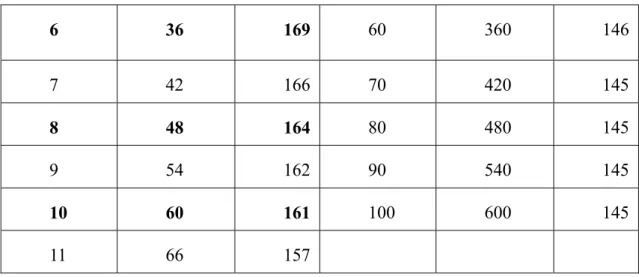
Table 3.1 Rise Time versus size of the MOS Transistors in Single-Stage Serializer.
13 . 0 3 . 1 ) L W ( p = 13 . 0 3 . 0 ) L W ( n = 13 . 0 3 . 1 ) L W ( p = 13 . 0 3 . 0 ) L W ( n = mp mn Tr mp mn Tr 1.0 6 302 12 72 157 1.1 6.6 292 13 78 157 1.2 7.2 276 14 84 157 1.3 7.8 265 15 90 155 1.4 8.4 257 16 96 154 1.5 9 250 17 102 154 1.6 9.6 245 18 108 154 1.7 10.2 240 19 114 153 1.8 10.8 234 20 120 152 1.9 11.4 228 21 126 150 2.0 12 223 22 132 149 3 18 198 30 180 148 4 24 181 40 240 147 5 30 175 50 300 146
Chapter 4 Transmitter Circuit Design 6 36 169 60 360 146 7 42 166 70 420 145 8 48 164 80 480 145 9 54 162 90 540 145 10 60 161 100 600 145 11 66 157
We describe the details of the cases for 300ps and 150ps.
300 ps case :
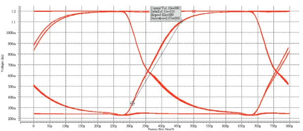
Figure 3.13 Eye Diagram of Rise Time of 300ps for Single-Stage Serializer.
Here, the area is referred to the total gate area.
2 N N p p N P N P m 0.13 117.8 0.13 6) 64 0.3 1 2 (1.3 L ) m NO. W m NO. (W Area 1.3163mW Power 6 m 1, m , m 0.13 m 0.3 ) L W ( , m 0.13 m 1.3 ) L W ( μ × = × × × + × × = × × × + × × = = = = μ μ = μ μ =
Chapter 4 Transmitter Circuit Design
150ps case:
Figure 3.14 Eye Diagram of Rise Time of 150ps for Single-Stage Serializer.
.3.2.2.2 Novel Tree-Type Serializer
We design and simulate this architecture according to Figure 3.15
2 N N p p N P N P m 0.13 2473.8 0.13 126) 64 0.3 21 2 (1.3 L ) m NO. W m NO. (W Area 17.614mW Power 126 m 21, m , n 0.13 m 0.3 ) L W ( , m 0.13 m 1.3 ) L W ( μ × = × × × + × × = × × × + × × = = = = μ μ = μ μ =
Chapter 4 Transmitter Circuit Design
Figure 3.15 Design steps for Novel Tree-Type Serializer.
In Step 1, we get the size of first stage 2-to-1 serializer that match the rising time specification by using the command .alter in HSPICE and carefully increase the size of MOS transistors. The result is shown in Table 3.2 and sizes that match the rising time specification are boldface.
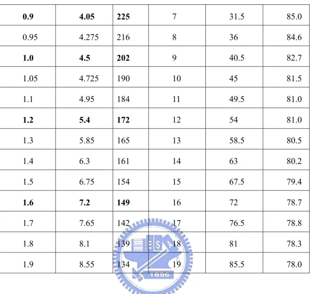
Table 3.2 Rise Time versus size of the MOS transistors in Novel Tree-Type Serializer. 13 . 0 3 . 1 ) L W ( p = 13 . 0 3 . 0 ) L W ( n = 13 . 0 3 . 1 ) L W ( p = 13 . 0 3 . 0 ) L W ( n = mp mn Tr (ps) mp mn Tr 0.6 2.7 320 2.0 9 130 0.65 2.925 297 3.0 13.5 106 0.7 3.15 280 3.7 16.65 100 0.75 3.375 261 4 18 95.9 0.8 3.6 248 5 22.5 90.9 0.85 3.825 235 6 27 89.1 Clock Data Skew DFF
Step1:Choose the size of the first stage MUX to
match the rising time spec.
Step4:Choose the size of Data Skew DFF to keep the rising time spec. Step5:Choose the size
of Clock Gen to keep the rising time spec.
Step3:Choose the size of the third stage MUX to match the rising time spec.
Step2:Choose the size of the second stage MUX to match the rising time spec.
Clock
Chapter 4 Transmitter Circuit Design 0.9 4.05 225 7 31.5 85.0 0.95 4.275 216 8 36 84.6 1.0 4.5 202 9 40.5 82.7 1.05 4.725 190 10 45 81.5 1.1 4.95 184 11 49.5 81.0 1.2 5.4 172 12 54 81.0 1.3 5.85 165 13 58.5 80.5 1.4 6.3 161 14 63 80.2 1.5 6.75 154 15 67.5 79.4 1.6 7.2 149 16 72 78.7 1.7 7.65 142 17 76.5 78.8 1.8 8.1 139 18 81 78.3 1.9 8.55 134 19 85.5 78.0
We describe the detail of the case of 300ps and 100ps for example.
300 ps case :
Chapter 4 Transmitter Circuit Design
100 ps case :
Figure 3.17 Eye Diagram of Rise Time of 100ps for Novel Tree-Type Serializer.
2 N N p p N P N P m 0.13 25.252 4 0.13 1) 12 0.156 1 2 (0.15 2 0.13 1) 12 0.156 1 2 (0.15 0.13 2.925) 12 0.3 0.65 2 (1.3 L ) m NO. W m NO. (W Area 1.3136mW Power 2.925 m 0.65, m , m 0.13 m 0.3 ) L W ( , m 0.13 m 1.3 ) L W ( μ × = × × × × + × × + × × × × + × × + × × × + × × = × × × + × × ∑ = = = = μ μ = μ μ = 2 7 1 mux mux N N p p N P N P m 0.13 82.592 4 0.13 1) 12 0.156 1 2 (0.15 2 0.13 1) 12 0.156 1 2 (0.15 0.13 16.65) 12 0.3 3.7 2 (1.3 L ) m NO. W m NO. (W Area 2.7900mW Power 16.65 m 3.7, m , m 0.13 m 0.3 ) L W ( , m 0.13 m 1.3 ) L W ( μ × = × × × × + × × + × × × × + × × + × × × + × × = × × × + × × = = = = μ μ = μ μ =
∑
=Chapter 4 Transmitter Circuit Design
.3.2.2.3 Conventional Tree-Type Serializer
The 8-to-1 conventional tree-type architecture is shown in Figure 3.18. We design and simulate this architecture according to Figure 3.15 which is the same to novel tree-type MUX.
Figure 3.18 8-to-1 conventional tree-type architecture.
As before, we show the rising time versus size of MOS transistors in Table 3.3 and sizes that match the rising time specification are boldface.
Table 3.3 Rise Time versus Size of the MOS Transistors in Conventional Tree-Type Serializer. 13 . 0 3 . 1 ) L W ( p = 13 . 0 3 . 0 ) L W ( n = 13 . 0 3 . 1 ) L W ( p = 13 . 0 3 . 0 ) L W ( n = mp mn Tr (ps) mp mn Tr (ps) 0.6 2.5 308 21 87.5 62.7 0.7 2.875 269 24 100 62.5 0.8 3.375 240 27 112.5 62.3 D1 D5 D4 D8 D3 D7 D2 D6 CLK/4 CLK/2 CLK=2.5G CLK/2 CLK/2 CLK/4 CLK/4 CLK/8 CLK/8
Chapter 4 Transmitter Circuit Design 0.9 3.75 215 30 125 62.5 1.0 4.125 201 33 137.5 62.2 1.1 4.626 183 36 150 62.3 1.2 5.0 171 39 162.5 62.7 1.3 5.375 163 42 175 62.9 1.4 5.875 153 45 187.5 62.7 1.5 6.25 145 48 200 62.2 1.8 7.5 130 51 212.5 61.8 2.1 8.75 118 54 225 62 2.4 10 109 57 237.5 63.4 2.7 11.25 102 60 250 62.4 3.0 12.5 97.4 63 262.5 62.7 6.0 25 74.7 66 275 62.8 9.0 37.5 68.4 69 287.5 62.8 12 50 65.4 72 300 63.4 15 62.5 64 75 312.5 63.3 18 75 62.7
We describe the detail of the case of 300ps and 100ps for example.
Chapter 4 Transmitter Circuit Design
Figure 3.19 Eye Diagram of Rise Time of 300ps for Conventional Tree-Type Serializer.
100 ps case :
Figure 3.20 Eye Diagram of Rise Time of 100ps for Conventional Tree-Type Serializer. 2 DFF P N 7 1 mux p p N N mux N P N P m 0.13 340.032 9 0.25 0.13 0.3) 88 1.3 (88 6 0.2 0.13 2.5) 12 0.3 0.6 2 (1.3 0.13 2.5) 12 0.3 0.6 2 (1.3 L ) W 88(W L ) m NO. W m NO. (W Area 3.2329mW Power 2.5 m 0.6, m , m 0.13 m 0.3 ) L W ( , m 0.13 m 1.3 ) L W ( μ × = × × × × + × + × × × × × + × × + × × × + × × = × + + × × × + × × = = = = μ μ = μ μ =
∑
∑
= 2 DFF P N 7 1 mux p p N N mux N P N P m 0.13 377.150 9 0.25 0.13 0.3) 88 1.3 (88 6 0.045 0.13 11.25) 12 0.3 2.7 2 (1.3 0.13 11.25) 12 0.3 2.7 2 (1.3 L ) W 88(W L ) m NO. W m NO. (W Area 3.9895mW Power 11.25 m 2.7, m , m 0.13 m 0.3 ) L W ( , m 0.13 m 1.3 ) L W ( μ × = × × × × + × + × × × × × + × × + × × × + × × = × + + × × × + × × = = = = μ μ = μ μ =∑
∑
=Chapter 4 Transmitter Circuit Design
3.2.3 The Comparison Results as Figures and Tables.
Figure 3.21 Area v.s. Rising Time.
Table 3.4 Power of three architectures versus Rising Time.
Rising Time Single-Stage MUX Conventional Tree Novel Tree Type 300ps 1.3163 3.2329 1.3136 275ps 1.6726 3.2618 1.3328 250ps 1.8246 3.2955 1.3706 225ps 2.0895 3.3722 1.4089 200ps 2.2480 3.3743 1.4479 175ps 3.5854 3.4486 1.5257 150ps 17.614 3.5068 1.5934 125ps X 3.6624 1.8391 Single-Stage MUX
Novel Tree-Type MUX Conventional Tree-Type MUX
Chapter 4 Transmitter Circuit Design
100ps X 3.9895 2.7900
Rising Time 170ps 165ps 160ps 155ps
Single -Stage 6.0694 7.2889 8.6057 12.326
Table 3.5 Area of three architectures versus Rising Time.
Rising Time Single-Stage MUX
Conventional Tree
Novel Tree Type
300ps 117.8x0.13um 340.032 x0.13um 25.252 x0.13um 275ps 141.36x0.13um 342.051 x0.13um 26.12 x0.13um 250ps 176.7 x0.13um 343.78 x0.13um 28.072 x0.13um 225ps 235.6 x0.13um 345.946 x0.13um 29.88 x0.13um 200ps 353.4 x0.13um 347.872 x0.13um 31.832 x0.13um 175ps 589 x0.13um 350.592 x0.13um 35.52 x0.13um 150ps 2473 x0.13um 354.482 x0.13um 43.112 x0.13um 125ps X 361.786 x0.13um 50.56 x0.13um
100ps X 377.150 x0.13um 82.592 x0.13um
Rising Time 170ps 165ps 160ps 155ps
Single-Stage MUX
Chapter 4 Transmitter Circuit Design Power v.s. Rising Time
Rising Time (ps) 50 100 150 200 250 300 350 Po wer (m W) 0 2 4 6 8 10 12 14 16 18 20 Single Stage Conventional Tree Novel Tree
Figure 3.22 Power v.s. Rising Time.
Area v.s Rising Time
Rising Time 50 100 150 200 250 300 350 Area 0 50 100 150 200 250 300 350 Single Stage Conventional Tree Novel Tree
Figure 3.23 Area v.s. Rising Time.
Table 3.6 Power X Area of three architectures versus Rising Time.
Rising Time Single-Stage MUX Conventional Tree Novel Tree Type 300ps 20.1578 142.9076 4.3122 275ps 30.7370 145.0413 4.5257
Chapter 4 Transmitter Circuit Design 250ps 41.9129 147.2805 5.0018 225ps 63.9972 151.6579 5.4727 200ps 103.2776 152.5972 5.9916 175ps 274.5341 157.1767 7.0451 150ps 5663.8698 161.6072 8.9303 125ps X 172.2507 12.0880 100ps X 195.6032 29.9561 Rising Time 170ps 165ps 160ps 155ps Single-Stage MUX 557.6807 892.9777 1317.8769 2831.4055
Power x Area v.s Rising Time
Rising Time 50 100 150 200 250 300 350 Pow er X Are a 0 1000 2000 3000 4000 5000 6000 Single Stage Conventional Tree Novel Tree
Chapter 4 Transmitter Circuit Design
Power x Area v.s. Rising Time
Rising Time 50 100 150 200 250 300 350 Po wer x Area 0 50 100 150 200 250 Conventional Tree Novel Tree
Figure 3.25 Power X Area v.s. Rising Time of Two Structures.
We use the data from Table 3.1, Table 3.2, and Table 3.3 to plot the Figure 3.21. From this figure, we can know the rising time limitation of each architecture due to the uncharged rising time of rapidly increased area. The rising time limitation of single-stage MUX is 150ps. The rising time limitation of novel tree-type MUX is 80ps. The rising time limitation of conventional tree-type MUX is 65ps. It also means the bandwidth limitation of each architecture and we can see the bandwidth of novel tree- type MUX is larger than single-stage MUX and a little less than conventional tree -type MUX.
Table 3.4 shows the power versus rising time of three architectures. Figure 3.22 is plotted from the data of Table 3.4. Table 3.5 shows the area overhead versus rising time of three architectures. Figure 3.23 is plotted from the data of Table 3.5. Table 3.6 shows the power area product versus rising time of three architectures. Figure 3.24 is plotted from the data of Table 3.6. Figure 3.25 shows only the power-area comparison of two tree structures. Here, area is referred to the total gate area.
Figure 3.22 and Figure 3.23 show that single-stage serializers can only go up to 6.5Gbps. Beyond 5Gbps, power and area increase significantly. Conventional tree-type and proposed tree-type serializers are able to reach 10Gbps with relatively constant power and area overhead. Due to these results of comparison, the advantages of low power and low area overhead over single-stage and conventional tree-type serializers are verified.
Chapter 4 Transmitter Circuit Design
Figure 3.26 Analysis vs. Simulation.
Table 3.7 Analysis vs. Simulation.
As following, we compare the result of simulations and analysis as Eq 6. We 5:1.2 5:0.97 Tr=175ps 2:0.9 2:0.74 Tr=225ps 1.2:0.7 1.2:0.58 Tr=275ps 1:0.65 1:0.53 Tr=300ps 1.5:0.8 1.5:0.65 Tr=250ps Tr=150ps Tr=200ps 21:1.6 21:1.16 3:1 3:0.85 Simulatoin mp8:mp2 Analysis mp8:mp2
mp8 v.s. mp2
mp8 0 5 10 15 20 25 mp2 0 1 2 3 mp2 (Analysis) mp2 (Simulation) 1560 m 95 . 1168 m 1440 : m m : m 8 p 8 p p8 2 p p8 = +Chapter 4 Transmitter Circuit Design
arrange the result as Table 3.7 and Figure 3.26 and verify the analysis in section 3.2.1 is matched the simulation.
3.3 Summary
In this chapter, we finish the analysis and comparison.
Table 3.8 shows the numerical data of power and area comparisons for five different rise time. Table 3.9 standardizes the performance using conventional tree as the reference. As one can see, the proposed design consumes 0.43 power and occupies 0.09 area of the conventional tree at 5Gbps (200ps rise time). Together, it is 25.84 times better than the conventional one. At 10 Gbps (100ps), the power and area ratio is 0.70 and 0.22. Performance wise, it is 6.49 times better.
Table 3.8 Power and Area Comparisons.
Single-Stage MUX Conventional
Tree Novel Tree Rise
Time
Power Area Power Area Power Area
100ps - - 3.99 49.03 2.79 10.74
150ps 17.61 321.59 3.51 46.08 1.59 5.60 200ps 2.25 45.94 3.37 45.22 1.45 4.14 250ps 1.82 22.97 3.30 44.69 1.37 3.65 300ps 1.32 15.31 3.23 44.20 1.31 3.28 Table 3.9 Power and Area Comparisons Standardizes by Using Conventional Tree.
Single-Stage
MUX Conventional Tree Novel Tree Rise
Time
Power Area Power Area Power Area 100ps - - 1 1 0.70 0.22
150ps 5.02 6.98 1 1 0.45 0.12
200ps 0.67 1.02 1 1 0.43 0.09
250ps 0.55 0.51 1 1 0.41 0.08
Chapter 4 Transmitter Circuit Design
Chapter 4
Transmitter Circuit Design
4.1 Introduction
This chapter will describe the detail circuit design of the chip implementation. Note that, 5GHZ VCO (voltage-controlled oscillator) is difficult to implement using 0.13um technology unless using a LC tank type oscillator. Without 5GHZ clock, the final stage is a 4-to-1 multiplexer, as will be shown in later. Since the test chip contains the serializer and a driver. There is no PLL on chip. Hence, the clock source is a 5GHZ clock. It is divided into a 4-phase 2.5GHz clock to emulate the 2.5GHZ PLL.
4.2 Circuit Design
Figure 4.1 is the whole architecture of this chip. It includes four 8-to-1 serializers, one 4-to-1 serializer and multi-stage driver. In this section, we describe the design of each block in detail and show the circuit.
Chapter 4 Transmitter Circuit Design
Figure 4.1 Whole architecture of the chip
4.2.1 MUX 8-to-1
There is no consideration about the propagation delay of each stage in Figure 3.3. But this is actually a design issue and we consider it here. In 0.13 mμ technology, a simple inverter with FO4 has 60ps propagation delay. Taking this delay into the 8-to-1 MUX of 2.5Gbps data rate, as Figure 3.4, we can see the timing diagram is shown in Figure 4.2. The Pn[1] and Pn[1]b are1.25GHz. The Pn[2], Pn[2]b, Pn[3] and Pn[3]b are through the first stage of frequency divider and have 625MHz. The Pn[4], Pn[4]b, Pn[5], Pn[5]b, Pn[6], Pn[6]b, Pn[7], and Pn[7]b which are through the second
Figure 4.2 Clock Diagram of 8-to-1 MUX with Propagation Delay
out Pn[1] Pn[2] Pn[3] Pn[4] Pn[6] Pn[4]b Pn[5]b Pn[5] Pn[1]b Pn[2]b Pn[3]b Pn[7]b Pn[6]b Pn[7] 8-1 8-1 8-1 8-1 D0~D7 D8~D15 D16~D2 D24~D31 Multi-phase Gen 312.5M PRBS 5GHz 4-phase 2.5GHZ 4-1 Driver
Chapter 4 Transmitter Circuit Design
stage of frequency divider have 312.5MHz. These clock frequency have the 60ps delay and so does the serializer. Figure 4.3 is the structure of 8-to-1 MUX and the data skew DFF as shown in figure. In conventional, we can use a positive and a negative trigger DFF to implement and we need twelve DFFs in 8-to-1 MUX. However, there is a more efficient way to implement. From [14~15] [17~23], we can use
Master-Slave-Master Flip Flop(MSM FF) to replace the positive and negative trigger DFF.The 90 phase shift between the inputs of serializer is achieved by adding an o
MSM-FF (extra latch) to one path.
Figure 4.3 Proposed Novel Tree-Type Serializer
Figure 4.4 Circuit of Differential DFF
Proposed Novel Tree MUX 8-to-1
CLK out 1.25G 625M 312.5M Skew M S M S M S ckb ck D Db Q Qb Diff DFF cell
Chapter 4 Transmitter Circuit Design
Figure 4.5 Structure of 8-to-1 MUX and Clock Gen
We use a new differential DFF as shown in Figure 4.4 for our clock generator and data skew DFF. This DFF has higher bandwidth and smaller area overhead than original one, as shown in Figure 3.11. This is because the fewer MOS transistors and less output node capacitance in this new differential DFF. The other reason we use this differential DFF is the requirement of 0 , o 90 , o 180 , o 270 phase of clock. o
Figure 4.5 show the structure of 8-to-1 serializer and clock generator. The circuit of each 2-to-1 MUX is shown in Figure 2.7(b). The corresponding data and clock diagram of each node is in Figure 4.6. Like Figure 4.2, Figure 4.6 adds the propagation delay time. The third stage 2-to-1 MUX outputs of novel tree-type MUX are net1, net2, net3, and net4 which are 625Mbps. The net1 multiplexes D1 and D5. The net2 multiplexes D2 and D6. The net3 multiplexes D3 and D7. The net4 multiplexes D4 and D8. The second stage 2-to-1 MUX outputs of novel tree-type MUX are net5, and net6 which are 1.25Gbps. The net5 multiplexes net1 and net3. The
D1 D3 D2 D Q D Q Q D D Q D Q Q D D Q Pn0 Pnb Pn[1] Pn[1]b Pn[2] Pn[2] Pn[3] Pn[3] Pn[4] Pn[4]b Pn[6] Pn[6] Pn[5] Pn[5]b Pn[7] Pn[1] Pn[1] D8 D5 D7 net1 net2 net3 net4 net5 net6 D4 D6 Out Pn[7]b
Chapter 4 Transmitter Circuit Design
net6 multiplexes net2 and net4. The first stage 2-to-1 MUX outputs of novel tree-type MUX are 2.5Gbps data rate. The out multiplexes net5 and net6..
Figure 4.6 Data and Clock Diagram of 8-to-1 MUX with Delay
4.2.2 Mux 4-to-1
Since the highest frequency of input clock rate is four phases 2.5GHZ, we use a 4-to-1 single-stage serializer to convert the four 2.5Gbps data rate to 10Gbps data rate. In [25], we know we can add an inductor in circuit to increase the bandwidth. This is called inductive peaking. The idea is to make the capacitance that limits the bandwidth resonate with the inductor. We describe the conception in detail as following. In Figure 4.7, the two circuits are common source stage with and without inductor peaking. If we have a input step pulse in Vi, the inductor in Figure 4.7 (d) serves as an open circuit since the components of high frequency in the transition of
Pn[1] Pn[2] Pn[3] Pn[4] Pn[6] Pn[4]b Pn[5]b Pn[5] Pn[1]b Pn[2]b Pn[3]b Pn[7] Pn[6]b Pn[7] Din[1:4] Din[5:8] Out
Realistic timing Diagram (Delay time:60ps)
net5 net6 net1 net2 net3 net4
Chapter 4 Transmitter Circuit Design
input step pulse. This causes the current all flow through the load C rather than through the resistor R. Thus, the output voltage level changes faster in Figure 4.7(c) than in Figure 4.7(a). The application is shown in [14~15][19][21][26~28].
As described above, inductive peaking can increase bandwidth substantially. But the area overhead due to inductor also increase rapidly. Thus, we overcome the drawback of low bandwidth of single-stage type by use active inductive peaking [24].
Figure 4.7 (a) CS Circuit with Load C (b) Small Signal Equivalent Circuit of (a) (c) CS Circuit with additional inductor (d) Small Signal Equivalent Circuit of (c)
Figure 4.8 Circuit of 4-to-1 MUX
O Ob d3 d2 d1 d4 P2 P1 P1 P4 P4 P3 P3 P2 d4b d1b d2b d3b P2 P1 P1 P4 P4 P3 P3 P2 4-1 MUX schematic i mV g Vi Vi R R C C L Vo Vo C C R R L i mV g Vo Vo (a) (b) (c) (d)
Chapter 4 Transmitter Circuit Design
Figure 4.9 Data and Clock Diagram of 4-to-1 MUX with Delay
The circuit of this 4-to-1 MUX is shown in Figure 4.8. We add an additional NMOS transistor as current source in each output node to enhance the inductance of active inductive peaking. . Figure 4.9 is the data and clock diagram of 4-to-1 MUX with delay.
4.2.3 MUX 32-to-1
Figure 4.10 Architecture of 32-to-1 MUX out D1 D3 D2 D4 P1 P3 P2 P4
4-1 MUX timing diagram
D4 D1 D2 D3 D4 D5 out D1 D2 D3 D4 D5 out D1 D2 D3 D4 D5 out D1 D2 D3 D4 D5 out D1 D5 D9 D13 D17 D21D25D29 D2 D6 D10 D14 D18 D22D26D30 D3 D7 D11 D15 D19 D23D27D31 D4 D8 D17 D16 D20 D24D28D32 D1 D2 D3 P1 P2 P3 P4 Out
Chapter 4 Transmitter Circuit Design
Figure 4.10 shows the overall circuit structure for the proposed 32-to-1 serializer for 10Gbps serial I/O. The module will be integrated into a 0.13um chip with an 8-phase 2.5GHz PLL.
4.2.4 Driver
For the requirement of measurement, we design a frequency divider to divide the input 5GHZ into four phases 2.5GHZ. And we design a multi-stage driver to drive the signal from 32-to-1 serializer. The circuit diagram is shown in Figure 4.11. This current mode logic (CML) driver is a conventional way in driver design [18] [20] [26~27] [29~30]. And the design skill is in [31]. This architecture has good immunity to SSN.
Figure 4.11 Architecture of Multi-Stage Driver
4.3 Simulation Result
Figure 4.12 is simulation result of the multi-phase generator output. It generates Pn[1] with 1.25GHZ, Pn[2], Pn[3] with 625MHZ, and Pn[4],Pn[5], Pn[6],Pn[7] with 312.5MHZ. These clocks are for 8-to-1 serializer and the simulation result is matched Figure 4.2. Figure 4.13 is the simulation of 8-to-1 serializer. It includes multi-phase clock, net1, net2, net3, net4 with 625Mbps data, net5, net6 with 1.25Gbps data, and out with 2.5Gbps data. This result is matched Figure 4.6. Figure 4.14 is the simulation result of 4-to-1 serializer. This serializer serializes four 2.5Gbps data from four 8-to-1 serializers to 10Gbps.
Figure 4.15 is the eye diagram of data through 32-to-1 MUX and multi-stage 500f
Chapter 4 Transmitter Circuit Design
driver. The data rate is 10Gbps. The output swing is 300mV. And the jitter is 3.66ps. Table 4.1 is the power consumption of each part of circuit. The total power consumption is 27.06mW. Figure 4.16 shows the effect of ground bounce to VDD and GND. The noise(P-P) is 40mV.
Figure 4.12 Simulation Result of The Multi-Phase Generator
Figure 4.13 Simulation Result of 8-to-1 Serializer. Pn[1 Pn[2 Pn[3 Pn[4 Pn[6 Pn[4] Pn[5] Pn[5 Pn[1] Pn[2] Pn[3] Pn[7] Pn[6] Pn[7] Pn[1] Pn[2] Pn[3] Pn[4] Pn[6] Pn[5] Pn[7] Din[1:4] Din[5:8] out net5 net6 net1 net2 net3 net4
Chapter 4 Transmitter Circuit Design
Figure 4.14 Simulation Result of 4-to-1 Serializer.
Figure 4.15 The Eye Diagram of 10Gbps Transmitter Table 4.1 The Power Consumption of Each Part of Circuit.
Module Current (mA) Power (mW) 8-1 MUX cell (4X)+ 4-1 MUX 2.7 3.24 4-phase 2.5GHZ 3.65 4.38 32bit_PRBS+multi-phase Gen 4.9 5.88 Driver 11.3 13.56 Total 22.55 27.06 o ouutt D D33 D D11 D D44 D D22 P P11 P P33 P P22 P P44
Chapter 4 Transmitter Circuit Design
Figure 4.16 The Effect of Ground Bounce to VDD and GND
4.4 Implementations
The chip has been implemented using TSMC 0.13um 2P8M CMOS process. It contains a 32-to-1 serializer, a 10Gbps driver, and a 32-bit PRBS (pseudo random bit sequence) generator. The diagrams of layout are shown in Figure 4.17 to Figure 4.23. The core area for the serializer is only 200um X 150um. The driver area is 360um X 110um. The total area of this chip is 1.14mm X 0.99mm.
Figure 4.17 Layout of MUX2 and DFF
Ground Bounce ~ 40mV (pk-pk)
Chapter 4 Transmitter Circuit Design
Figure 4.18 Retiming and PRBS DFF
Figure 4.19 8-to-1 MUX
Figure 4.20 (a) Clock Generator for 8-to-1 MUZ (b) 4-to-1 MUX (c) 5GHZ to four phase 2.5GHZ Clock divider
M Maasstteerr S Sllaavvee M Maasstteerr S Sllaavvee M Maasstteerr M MUUXX MMUUXX22 MMUUXX22 MMUUXX22 M MUUXX22 MMUUXX22 M MUUXX22 (a) (b) (c)
Chapter 4 Transmitter Circuit Design
Figure 4.21 32-to-1 Serializer
Figure 4.22 Layout of Whole Chip (Without Dummy) gndd gndd gndd gndd ck e ckb e s r vdd2 vdd1 vdd3 vdd4 gnda gnda gnda gnda outb out