國 立 交 通 大 學
電子工程學系 電子研究所
碩 士 論 文
於3.1-10.6GHz無線應用的超寬頻金氧半功
率放大器
An Ultra-Wideband CMOS Power Amplifier
for 3.1 to 10.6 GHz Wireless Applications
研究生: 陳科閔
指導教授: 荊鳳德 博士
於3.1-10.6GHz無線應用的超寬頻金氧半功率放大器
An Ultra-Wideband CMOS Power Amplifier for 3.1 to
10.6 GHz Wireless Applications
研 究 生:陳科閔 Student: Ke-Min Chen
指導教授:荊鳳德 博士 Advisor: Dr. Albert Chin
國立交通大學
電子工程學系 電子研究所碩士班
碩士論文
A Thesis
Submitted to Department of Electronics Engineering & Institute of Electronics College of Electrical Engineering and Computer Science
National Chiao Tung University in Partial Fulfillment of the Requirements
for the Degree of Master
in
Electronics Engineering
June 2006
HsinChu, Taiwan, Republic of China
中華民國九十五年六月
於3.1-10.6GHz無線應用的超寬頻金氧半功
率放大器
學生: 陳科閔
指導教授: 荊鳳德 博士
國立交通大學
電子工程學系電子研究所
摘要
本論文以 TSMC 0.18um 的 CMOS 製程環境下,首先設計了一個兩級在 3.1 到 10.6GHz 的超寬頻功率放大器。第一級在共源、共閘的串疊結構之中,加入了電 阻的迴授結構。這樣帶來了高的功率增益以及寬頻的輸入組抗匹配:而第二級利 用了共源加上電阻電感迴授的結構,來達到寬頻組抗匹配以及平坦的功率增益。 接下來針對上述的功率放大器研究後,我們改進了設計的細節,進一步設計了 一個 3 到 8GHz 的兩級超寬頻功率放大器。藉由將電容加入上述的迴授結構,我 們減少了在迴授路徑上面的直流功率消耗。再加上對負載線設計的加強,我們在 線性度以及功率轉換效益上有很大的突破。An Ultra-Wideband CMOS Power Amplifier for
3.1 to 10.6 GHz Wireless Applications
Student: Ke-Min Chen
Advisor: Dr. Albert Chin
Department of Electronics Engineering & Institute of Electronics
Nation Chiao Tung University
Abstract
This thesis is based on TSMC 0.18um CMOS process. A two-stage ultra-wideband CMOS power amplifier is applied for 3.1 to 10.6GHz. The 1st stage introduces the
common-source and common-gate topology called “cascade” with the resistor feedback configuration. It brings higher power gain and wideband input impedance match. And the 2nd stage utilizes the common-source with resistor and inductor in
order to wideband matching and power gain flatness.
After further studying for the above-mentioned power amplifier, we improve the detail and design a two-stage power amplifier for 3 to 8GHz. By adding a capacitor to the feedback path, both feedback configurations at the 1st and 2ndstages decreases the
DC power loss. And we obtain more suitable DC bias condition by focusing on the load-line design; it does work very much to our efficiency and linearity.
Acknowledgement
這篇論文能夠順利完成,首先得感謝我的指導教授-荊鳳德老師。在老師的細 心引導、諄諄教誨之下,讓學生對於碩士研究有了深刻的心得,而論文寫作提供 寶貴的意見,給予學生的收穫更是銘記在心,不可言喻。科閔在這邊表達最誠摯 的感謝。 接著,科閔也非常感謝學長姐、同學、學弟妹對我的扶持與照顧。尤其感謝殿 聖及存甫學長在我不順遂時陪我解惑、一起度過艱困的生活,感謝軍宏、建宏學 長、瑄苓學姊在生活大小事中都能給予適時的建議、分享與幫助;感謝秋峰、照 民及櫸檀學長在學業上的幫助與指導,感謝張慈學長在研究上提供意見的幫助甚 多,使論文能夠具體而微的建立起來。 感謝香谷對我優缺點多所針砭鼓勵,你的話語帶給我信心;感謝鴻瑋課業上的 幫助以及生活的分享,你優質的品味總是給我很多不同的想法;感謝泰瑞如沐春 風般的貼心關懷,我很需要的; 感謝一年的室友國慶,室友的緣分與對我的幫 助文字絕對不足以形容。 感謝學弟妹哲緯、冠麟、俊全、偉倫、正彥、懿範、佩諭,相處的一年對科閔 的嘮叨多所包含,下學年度就換你們畢業了,請加油! 最後,感謝一路走來無條件支持陪伴我的父母、我的兄姊,有了你們才有今天 的科閔。未來的人生路上我會用行動證明,科閔值得你們繼續支持! 謹將這篇碩士論文獻給所有在身旁關懷我的人,十分感謝大家。Contents
Abstract (in Chinese)
………IAbstract (in English)
………...IIAcknowledgement
……….…..IIIContents
……….IVFigure Captions
………..VIIIChapter 1 Introduction
1.1 Motivation
………1Chapter 2 Basic Concepts of Power Amplifiers
2.0 Introduction
2.1 Amplifier Parameter Definitions
………32.1.1 Weakly Nonlinear Effects: Power Series Analysis
………42.1.2 Strongly Nonlinear Effects
………..…62.1.3 Nonlinear Device Models for CAD
………..72.1.4 Gain Match and Power Match
………...82.1.5 Knee voltage effect
………...92.1.6 Load-Pull Measurement
……….102.1.8 Power gain
……….122.1.9 Output Power and P
1dB………...122.1.10 Power Added Efficiency (PAE), Drain Efficiency (ηd),and
Power Utilization Factor
………122.1.11 Spectral Regrowth
……….132.1.12 Adjacent Channel Power Ratio (ACPR)
……….142.1.13 Peak-to-Average Ratio (PAR)
………142.1.14 Nonlinearity Effect in Power Amplifier Use Two-tone
Analysis
………..152.1.15 AM-to-PM Effect
………..162.2 Class of Power Amplifiers
………172.2.1 Class A, AB, B, and C Power Amplifiers
……….182.2.2 Class D, E and F Power Amplifier
………..212.2.3 Power Amplifier Stability Issues
……….222.3 Challenges of RF Power Amplifiers in CMOS Technology
…………..232.3.1 Low Breakdown Voltage of Deep Sub-micron Technologies
…...232.3.2 Substrates Coupling Effects
………..232.3.3 Large Signal CMOS RF Models
……….232.3.5 Electro-migration and Reliability of CMOS Devices
………24Chapter 3 Basic Power Amplifiers Design
3.1 General consideration in RF Amplifiers
……….263.1.1 Stability
………...263.1.2 Impedance matching
………273.1.3 Special Topic for Output: Load-line Match
………...333.2 Conventional RF power amplifier design
………...343.2.1 Starting at LNA
……….343.2.2 Wide-band amplifier design
………...35Chapter 4 UWB CMOS Power Amplifier design
4.1 The PA Issues of UWB Transmitter
………..404.2 UWB Design for CMOS Power Amplifier
………414.2.1 Input Matching: Cascode with Resistor Feedback
………..414.2.2 Output Matching with Inductor-resistor Feedback
……….434.2.3 Gain flatness of amplifier with inductor-resistor feedback
……...454.2.4 Detail of the Power Amplifier for UWB application
………..474.2.5 Simulation Results
………..494.3 Further Design for Better Efficiency and Linearity
………534.3.1 Further Design by Load-line Curve
………544.3.2 Simulation for Further Design
……….564.3.3 Layout of The Further Design
………...59Chapter 5 Summary
………...60Figure Captions
Chapter 1 Introduction
Chapter 2 Basic Concepts of Power Amplifiers
Figure2-1: Conjugate match and load-line match.
Figure2-2: The knee voltage of deep sub-micron CMOS transistor. Figure 2-3: Typical configuration of load-pull.
Figure2-4: The spectral regrowth due to amplifier nonlinearity. Figure 2-5: The phase-shift distortion with input power increases. Figure 2-6: The classification of Power amplifier.
Figure 2-7: Reduced conduction angle current waveform.
Figure 2-8: Fourier component of power amplifier relate to conduction angle.
Figure 2-9: RF power and efficiency with conduction angle sweep; assume optimum load and harmonic short.
Chapter 3 Basic Power Amplifiers Design
Figure 3-1: Stability of two-port networks. Figure 3-2: Circuit embedded in a 50-Ω system. Figure 3-3: A possible impedance-matching network.
Figure 3-5: Which ell matching networks will work in which regions. Figure 3-6: (a) A discrete RF amplifier; (b) the dc model; (c) the ac model. Figure 3-7: The load with the load-line matching network.
Fig. 3-8: Common source stage use inductance degeneration. Figure 3-9: A wide-band LNA circuit schematic.
Figure 3-10: Another wide-band LNA schematic.
Figure 3-11: Small-signal equivalent circuit at the input.
Chapter 4 UWB CMOS Power Amplifier design
Figure 4-1: The power level of UWB.Figure 4-2: The input stage of our PA.
Figure 4-3: The small-signal equivalent circuit at the input. Figure 4-4: The output stage of our design.
Figure 4-5: The I-V curve of the load-line study of the PA.
Figure 4-6: The comparison with the value of the feedback resistor.
Figure 4-7: The |S21| of “common-source with RL feedback” and “two stages overall”.
Figure 4-8: The overall schema of our UWB PA. Figure 4-9: The S-parameter of the PA.
Figure 4-10: The Noise Figure. Figure 4-11: The stability index: Mu.
Figure 4-12: The performance of PA in the aspect of linearity. Figure 4-13: The layout of the PA.
Figure 4-14: The further design of PA. Figure 4-15: The output stage of the PA.
Figure 4-16: (a) The 50Ω-line and opt-line. (b) The load-line analysis by ADS tools. Figure 4-17: The S-parameter of the PA.
Figure 4-18: The Noise Figure. Figure 4-19: The stability index: Mu.
Figure 4-20: The performance of PA in the aspect of linearity. Figure 4-21: The layout of the PA.
Chapter 1
Introduction
1.1 Motivation
For portable wireless communication devices has given great push to the development of a next generation of low power radio frequency integrated circuits (RFIC) product. Such as wireless phones, cordless and cellular, global positioning satellite (GPS), pagers, wireless modems, wireless local area network (LAN), and RF ID tags, etc., require more low cost; low noise and high power efficiency solutions to supply the demand for low-price product [1].
In UWB systems, the power level from the UWB transmitter should be low enough not to interfere with the already existing communication systems, for example 802.11a. The low output levels that specified by the Federal Communications Commission (FCC) is less than -41.3 dBm/MHz. Therefore, for a 7 GHz bandwidth, the peak output power is approximately-3 dBm or 500μW. UWB systems need not require large transistors, and greatly lighten the difficult of CMOS technology. The main challenging task becomes to achieve a high gain and good impedance match over the entire frequency band.
The RF integrated circuit used for UWB devices are encounter with various possibilities: CMOS, Bi CMOS, and GaAs MESFET, bipolar (BJT), hetero-junction
bipolar transistor (HBT), and PHEMT, etc,. We just study and discuss on the CMOS technology.
Chapter 2 discusses the basic concepts of power amplifier. Chapter 3 presents the basic power amplifiers design for UWB. Chapter 4 deals with wideband matching network, gain flatness and load-line analysis by using inductor-resistor feedback, presents the UWB proposals, design, implementation of our power amplifiers. Chapter 5 concludes this research effort with some future directions.
Chapter2
Basic concepts of Power Amplifier
2.0 Introduction
A reasonable start of power amplifier, which is abbreviated as PA, would be to recall some classical results of linear RF amplifier theory because many PA designs are simple extensions or modifications of linear design. We can read the detail results of RF linear amplifier in many books, so we skip those and assume some concepts of RF linear amplifier is well known.
As we discuss about power amplifier, some basic concepts should be motioned. First, the PA operates at a high out power state; for example, CMOS devices could be saturated, and therefore nonlinear effect become significant. If the output power is 1Watt, and how much power the PA should be dissipated? Ideally, we want all the DC supply power be converted to signal power, but it is impossible in practice. Therefore the efficiency is the important performance of PA. And some issues about optimum output power should be studied including load line match and load-pull technology. So, this chapter presents the main concepts and challenges of RF power amplifiers.
2.1 Amplifier Parameter Definitions
2.1.1 Weakly Nonlinear Effects: Power Series Analysis
aspects, but it has some limitations: there is no phase component in the linear output term, letting alone the nonlinear terms. A much stronger formula of the power series, called the Volterra series, would be used including phase effects. Weak nonlinearities may be, for instance, inter-modulation distortion at levels lower than, say, -30dBc. Unfortunately, the PA operating at or beyond the compression point requires different treatment because the nonlinearities become “strong” and arise through the cutoff and clipping behavior of the transistor; besides, the Power and Volterra series is not sufficiently accurate. The fifth and seventh order terms of Power series usually become significant as the 1dB compression point is approached and can dominate at still higher drive levels.
While plenty of RF amplifiers can be described as a linear model to obtain their response of small signals, nonlinearities often lead to interesting and important phenomena. Generally, the “Power Series” is applied to further analysis. For simplicity, we ignore the higher order terms of the series and assume that
y
(
t
)
≈
α
1x
(
t
)
+
α
2x
2(
t
)
+
α
3x
3(
t
)
(2.1) If a sinusoid is applied to a nonlinear system, the output generally exhibitsfrequency components that are integer powers of the input frequency. If
x
(
t
)
=
A
cos
ω
t
, thent
A
t
A
t
A
t
t
A
t
A
t
A
A
A
α
α
ω
α
ω
α
ω
α
3
cos
4
2
cos
2
cos
4
3
2
3 3 2 2 3 3 1 2 2+
+
⎟⎟
⎠
⎞
⎜⎜
⎝
⎛
+
+
=
(2.3)In Eq. (2.3), the term cos tω is called the “fundamental” and the higher-order terms the “harmonics.” The amplitude of the nth harmonic, cosnωt, consists of a term
proportional to An.
In (2.3), the gain written as
4 3 2 3 1 A
α
α
+ is therefore a decreasing function of Aifα3<0. In most circuits, the output is a “compressive” or “saturating” function of the
input; that is, the gain approached zero for sufficiently high input levels. This effect is quantified by the “1-dB compression point,” defined as the input signal level that causes the small-signal gain to drop by 1 dB. If it’s plotted on a log-log scale as a function of the input level, the output level falls below its ideal value by 1 dB at the 1-dB compression point.
When two signals with different frequencies are applied to a nonlinear system, the output in general exhibits some components that are not harmonics of the input frequencies. Called inter-modulation (IM), this phenomenon arises from
multiplication of the two signals when their sum is raised to a power greater than unity. We assume that
x
(
t
)
=
A
1cos
ω
1t
+
A
2cos
ω
2t
(2.4) Thus,y
(
t
)
=
α
1(
A
1cos
ω
1t
+
A
2cos
ω
2t
)
+
α
2(
A
1cos
ω
1t
+
A
2cos
ω
2t
)
23
)
cos
cos
(
3
ω
ω
α
+
+
Expanding the left side and discarding DC terms and harmonics, we obtain the inter-modulation products:
t
A
A
t
A
A
)
2
cos(
4
3
)
2
cos(
4
3
:
2
2 1 2 2 1 3 2 1 2 2 1 3 2 1ω
ω
α
ω
ω
α
ω
ω
ω
→
±
+
+
−
(2.6)t
A
A
t
A
A
)
2
cos(
4
3
)
2
cos(
4
3
:
2
1 2 1 2 2 3 1 2 1 2 2 3 1 2ω
ω
α
ω
ω
α
ω
ω
ω
→
±
+
+
−
(2.7)Because the difference between ω1 and ω2 is small, the components at
2ω1-ω2 and 2ω2-ω1 appear in the vicinity of ω1 and ω2. In a typical two-tone test,
A1=A2=A, and the ratio of the amplitude of the output third-order products to α1A
defines the IM distortion. If a weak signal accompanied by two strong interferers experiences third-order nonlinearity, then one of the IM products falls in the band of interest, corrupting the desired component.
Use IP3 to characterize this behavior. Called the “third intercept point” (IP3), this
parameter is measured by a two-tone test in which A is chosen to be sufficiently small so that higher-order nonlinear terms are negligible and the gain is relatively constant and equal toα1. The third-order intercept point is defined to be at the intersection of
the two lines [2].
2.1.2 Strongly Nonlinear Effects
Strongly nonlinear effects refer to the distortion of the signal waveform that is caused by the limiting behavior of the transistor. The drain current exhibits cutoff, or
pinch-off, when the channel is completely closed by the gate-source voltage and reaches a maximum, or open-channel condition, in which further increase of gate-source voltage results in little or no further increase in drain current.
2.1.3 Nonlinear Device Models for CAD
To devise a comprehensive model for a device, it is necessary to characterize both the weak and the strong nonlinear behavior. Unfortunately, each of the nonlinearity traits in a particular device arises from quite different aspects of the device physics. The PA designer is much more sensitive to some of the shortcomings of widely used computer-aided design (CAD) models than designers of many other kinds of RF devices. The central issue in modeling RF power transistors is scaling. The detailed modeling and curve fitting are done on a small periphery sample device and may be quite accurate. The PA designer has to take that small cell and scale up it, even hundreds, to “build” a power transistor. Unfortunately, such scaling is not a simple set of electrical nodal connections, and can not be handled easily enough on a modern circuit simulator. The large periphery device will display a range of secondary phenomena that may have been quite negligible in the small periphery device model cell. The low impedance by multiple parallel connections evokes other-effects to come, that would be neglected in normally, including current spreading at bond-wire contacts, electro-acoustic coupling in the semiconductor crystal, and mutual coupling
between bond-wire.
Even a basic I-V measurement can pose serious difficulties for an RF power transistor. Mary I-V curve tracers work at speeds several slower than the RF signal for which the model is require and can be slow enough that transient junction heating effects, which will not occur to any significant extent during an RF cycle, intrude into the measurement. Accurate I-V curve are difficult to obtain for RF power transistors; that has led many to develop custom-built teat rigs, usually incorporating a pulsed measurement scheme [10]. An alternative approach is to build a curve tracer that sweeps through the I-V characteristics at rates in RF range [9].
Reference [11], [12], [15-17] provides starter bibliography, but the research continues.
2.1.4 Gain Match and Power Match
We can get the maximum gain when input and output of circuits was conjugate match. It is well known by circuit theorem that we can deliver maximum power into load component when load impedance is equal to real part of the generator impedance, and the reactive part should be resonated out. This is the concept of conjugate match or gain match. However, the practical devices have physical limited such as Vmax and
Imax, the maximum supply voltage and the maximum generated current. Vmax could be
saturation current of devices. By referring Figure 2-1, this seen the gain match cannot used the full capacity of transistor. If we want to utilize the maximum current and voltage swing of the transistor, a lower value of load resistance would need to be selected; the value is commonly referred to as the load-line match, Ropt, and in its simplest form simply would be the ratio:
max max
/ I
V
R
opt=
(2.8)Where we assume the generator’s resistance is high and is not taken into account. This Ropt is so called the load-line match or power match. The power match represents a
real compromise that is necessary to extract the maximum power from RF transistors and at the same time keep the RF voltage swing within specified limits and the available dc supply.
2.1.5 Knee voltage effect
The knee voltage (pinch-off voltage) divides the saturation and the linear region of the transistor and can be defined as, for example, Vds at the 95% of Imax point. As shown
in Figure 2-2[18]. And the optimum load resistance become
max
max
)
/
(
V
V
I
R
opt=
−
knee (2.9)For sub-micron CMOS transistors, Vknee is only about 10% to 15% of the supply
voltage for typical power transistors, while it can be as high as 50% of the supply for deep sub-micron technologies as shown in Figure 2-2. A large portion of the RF cycle could be in linear region. Accordingly, both saturation and linear region must be considered when determining the optimum of operation [18] or relying on balance simulations of circuits.
2.1.6 Load-Pull Measurement
A load-pull test setup consists of the device under test with some form of calibrated tuning device on its output. A typical block diagram is shown in Figure 2-3.
Figure 2-3: Typical configuration of load-pull.
The input probably also will be tunable, but this is mainly to boots the power gain of the device, and the input match typically be fixed close to a good match at each frequency.
Load-pull measurement can find the practical Ropt of PA, and also the maximum
output power.
2.1.7 Input and Output VSWR
VSWR are measured at small-signal conditions as well as at large-signal conditions. There come some problems with power match, It will cause reflections and VSWR at output, the reflected power is entirely a function of the degree of match between the antenna and the 50-Ohm system. The PA does not present a mismatched reverse
large signal impedance, once a device starts to operate in a significantly nonlinear fashion, the apparent value of the impedance will change, but the whole concept of impedance starts to break down as well, because the waveforms no longer are sinusoidal.
2.1.8 Power gain
The power amplifiers are characterized by transducer power gain defined as the ratio of the power delivered to the load (Po) to the power available from the source
(Pin) to the amplifier, i.e.,
in
o
P
P
G
=
/
(2.10)2.1.9 Output Power and P
1dBPower delivered to the load (Po) is known as the output power, which is a strong
function of the input power. The output power when the gain is compressed by 1 dB is defined as P1dB, which is normally used as a figure of merit to characterize
nonlinearity in amplifiers.
2.1.10 Power Added Efficiency (PAE), Drain Efficiency (ηd),and
Power Utilization Factor
The PAE is defined as
_ _ _ _
_
1 1
(1 ) (1 ).
output signal power input signal power Po Pin PAE dc power Pdc Po PAE d Pdc G η G − − = = = − = − , (2.11)
where ηd is known as the drain efficiency. For high-efficiency amplifiers, single-stage gain is required to be on the order of 10 dB or higher. If the RF power gain is less than 10 dB, the drive power requirement will start to take a serious bite out of output efficiency of a PA stage, and the higher the efficiency, the more serious the effect. Sometimes, it is just as well to keep gain and output efficiency as separate stage, it is noted that at system level or even multistage PA level they will behave interactively on the overall efficiency.
One of the most importance concepts in comparing different PA configurations is the power utilization factor (PUF). PUF is the ratio of the power it would deliver as a simple class A amplifier.
_ P rf PUF Plin = , (2.12) * 4 Vdc Ipk Plin= , (2.13)
where Plin is known as the output power of class A having the same dc supply voltage and peak RF current.
2.1.11 Spectral Regrowth
In a digitally modulated waveform, for example, QPSK, need a low-pass filter precede the modulator to limit the bandwidth of the signal, there by suppressing spectral leakage into adjacency channels. We expect limiting the bandwidth tends to smooth out the abrupt transitions in the time domain. And after filtering, exhibiting
variation in its envelope as the filter bandwidth decreases. If the power amplifier is to maintain the spectrum to the limited bandwidth, then it must also amplify the envelope variations linearly. However, if the PA exhibits significant nonlinearity, then shape signals, it is not preserved and the spectrum is not limited to the desired bandwidth. This effect is called “spectral regrowth” [19], [20] and can be quantified by the relative adjacent channel power [20]. Generally, nonlinear PA has better efficiency than linear PA. Therefore, digital modulation schemes exhibit a trade-off between spectral efficiency and power efficiency.
Figure2-4: The spectral regrowth due to amplifier nonlinearity.
2.1.12 Adjacent Channel Power Ratio (ACPR)
[21]
ACPR is a commonly used figure of merit to evaluate the inter-modulation performance of RF power amplifiers designed for CDMA wireless communication systems, ACPR is a measure of spectral regrowth, appears in the signal sidebands, and
is analogous to IM3/IM5 for an analog RF amplifier.
_ _ _ _ _ _ _1
_ _ _ _ _ _ _ 2 3
power spectral density in the main channel ACPR
power spectral density in the offset channel or
=
, (2.14) There offset frequencies and measurement bandwidths vary with system application.
2.1.13 Peak-to-Average Ratio (PAR)
[22]
All single or multi-carrier (modulated or un-modulated) have a peak-to-average ratio. The ratio between the peak power (Pp) and the average power (Pa) of a signal is
called the peak-to-average ratio, i.e.,
,10log ( ) Pp Pp dB Pa Pa χ = . (2.15) The peak-to-average ratio ΔPs of an input signal consisting of N carriers, each having
a average power Pί is defined as
2 1 1 ( ) n i i i n i i P Ps P χ = = Δ =
∑
∑
. (2.16) Here χi is the peak-to-average ratio of the ith carrier. If there are n carriers in a givenoperating bandwidth, it is easy to see that the theoretical maximum peak-to-average power ratio will be n . Gaussian noise has a peak-to-power ratio of about 9 dB, so very dense multi-carrier systems might require about 6 dB more power back-off to achieve a similar level of IM distortion compared to a two-carrier signal having the same power.
2.1.14 Nonlinearity Effect in Power Amplifier Use Two-tone Analysis
There many different ways to measure the nonlinearity behavior of an amplifier. The simplest method is the measurement of the 1dB compression power level P1dB. Another method that uses two closely spaced frequencies:1 2
( )
cos(
)
cos(
)
Vi t
=
v
ω
t
+
v
ω
t
(2.17) Vi input to amplifier and measure the output frequencies component, this is so-call the
inter-modulation (IM) products. The third-order products are at frequencies
2ω
2-ω
1 and2ω
1-ω
2, and the fifth-order IM products are at frequencies3ω
2-2ω
1 and3ω
1-2ω
2. The third-order Intercept point (IP3) is a concept that represents the intersection between the extrapolated 1:1 slope of fundamental gain, and the 3:1 slope of the third-order IM (IM3) products. IM3 is given by[23]:1 2 2 1 1 2 2 2 3( ) P P 2( 3 f) IM dBc IP P P P ω ω ω ω ω ω − − = = = − , (2.18)
where Pf (dBm) is the average value of Pω1 and Pω2 .
Another “softness” of the compression characteristic can be varied by choosing two tangible parameters, PCOMP and PSAT. PCOMP represent, in decibels, the different
between the P1dB compression point and the maximum linear power point; PSAT
represent, in decibels, the different between the saturated power point and the maximum linear power point, about this value, the characteristic is defined to be ideally flat, or saturated. The detail discuss of nonlinear effect can be studied at[24].
2.1.15 AM-to-PM Effect
Any amplifier, when driven into a strongly nonlinear condition, will exhibit phase as well as amplitude distortion.
Figure 2-5: The phase-shift distortion with input power increases.
This usually is characterize in terms of AM-to-PM conversion and represents a change in the phase of the transfer characteristic as the drive level is increased toward and beyond the compression. The most common manifestation of AM-to-PM effects is an irritating asymmetrical slewing of the inter-modulation (IM) or spectral regrowth display. The detail discuss of AM-to-PM effect can be studied at[24].
2.2 Class of Power Amplifiers
What determine the class of operation of power amplifier is conduction angle of amplifier, input signal overdrive, and the output load network. Figure 2-6 shows how the PA relates to conduction angle and the input signal over-drive. For a small RF input signal Vin, the amplifier can operate in class A, AB, B, or C depending on the
Figure 2-6: The classification of Power amplifier.
The PA efficiency can be improved by reducing its conduction angle by moving the design into class C operation, but at the expense of lower output power. An alternative approach to increasing efficiency without sacrificing output power is to increase the input over-drive such that the transistor acts as a switch.
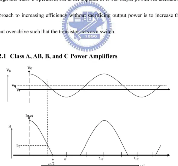
2.2.1 Class A, AB, B, and C Power Amplifiers
VO Iq IMAX Vt Vq π 2π 3π α/2 ωt id Vg VO Iq IMAX Vt Vq π 2π 3π α/2 ωt id VgThe simple process of reducing the conduction angle is illustrated in Figure 2-7, where Vt is the threshold voltage of Vgs for transistors. The required signal voltage
amplitude will be
1
s q
V
= −
V
(2.19)Where Vq is the normalized quiescent bias point, defined according to Vt=0, Vo=1. The current in the device has the familiar looking, truncated sine-wave appearance. The conduction angle, α, indicates the proportion of the RF cycle for which conduction occurs, the current cutoff points point are at ±α/2. So the drain current waveform can be written as
cos ___ / 2 / 2 0 ____________ / 2; / 2 d q pk d i I I i θ α θ α π θ α α θ π = + − < < = − < < − − < < , (2.20)
By Fourier analysis of the waveforms, the results can be written:
/ 2
max / 2
1
[cos cos( / 2)]cos
2 1 cos( / 2) I In α n d α θ α θ θ π − α = − −
∫
, (2.21) then it is clear thatmax max I 2sin( / 2) cos( / 2) 2 1 cos( / 2) sin 2 1 cos( / 2) fundamental Idc I I α α α π α α α π α − = − − = − ,. (2.22), (2.23)
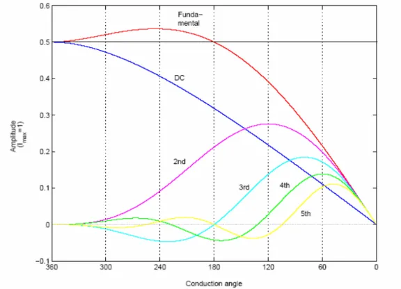
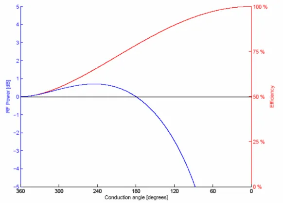
We use the conduction angle to define the class of power amplifier, for class A condition, α=0; for class B condition, α=π; for class AB condition, 0<α<π; and for the condition of class C, α>π. The harmonics amplitude is plotted in Figure 2-8.
Figure 2-8: Fourier component of power amplifier relate to conduction angle. We can see the odd harmonics be seen to pass through zero at the class B point, but in AB mode, the third harmonic is not negligible.
Then, the RF fundamental output power is given by 1 1 2 2 Vdc I P Pdc VdcIdc = = , (2.24), (2.25) the output efficiency is defined by:
1
P Pdc
η =
, (2.26) then we can plot the result on Figure 2-9. From this Figure the main features of class A, AB, B and C can be determined.
Figure 2-9: RF power and efficiency with conduction angle sweep; assume optimum load and harmonic short.
2.2.2 Class D, E and F Power Amplifier
In this class the active device works as a switch; with very low resistance in the “ON” state and very high impedance in the “OFF” state, and respect to the load impedance. If the “ON” resistance is negligible, no power dissipation in the device and if the “OFF” impedance is very large, no current flows through the device. Therefore, in an ideal switching amplifier one can achieve 100% drain efficiency. The different between a class D and a class E is that a class E amplifier has a high Q-tuned circuit at the output of the device provide desired reactive load at the fundamental frequency and open to other higher harmonics.
A class F amplifier is designed in the same manner as a class AB/B amplifier, except that the output circuit is designed to present a short circuit to the second harmonic and an open circuit to the third harmonic. The output waveform could become a square, such as a switch, and the theoretical efficiency approaches 100%. Switch mode power amplifier in practice, efficiency could be degraded because the finite ON resistance and also there is significant transition time from the ON state to the OFF state and vice versa.
2.2.3 Power Amplifier Stability Issues
General speaking, k-factor analysis is useful to a linear two-port devices, it is usually a satisfactory assumption to assume that RF oscillations in power amplifiers will more likely occur when the amplifiers is backed off into its linear region, where the k-factor analysis is valid. At the condition of class AB or B operation, it is necessary to increase the quiescent current to perform the stability analysis with a represent amount of gain.
Stability of multi-stage amplifier is usually used k-factor analysis of individual stages. Any single stage must be designed with k-factor greater than unity from the low-frequency bias circuit range all the way up to the frequency at the gain rolls off to lower than unity. The use of resistive element will affect the efficiency of the PA, and is an effective way to obtain good stability performance.
2 2 2 1 11 22 , 11* 22 12* 21 2 11 12 S S D k D S S S S S S − − + = = − ,. (2.27)
2.3 Challenges of RF Power Amplifiers in CMOS Technology
CMOS technology is not friendly towards design of power amplifiers. We simple list some issues that affected the PA performance.
2.3.1
Low Breakdown Voltage of Deep Sub-micron Technologies.
This limits the maximum gate-drain voltage and delivering lower power. Unfortunately, COMS technology has lower current drive, the single stage gain is very low, and multiple stages would be used but affect the linearity and efficiency of amplifiers.
2.3.2
Substrates Coupling Effects
In contrast to semi-insulating substrates, a highly doped substrate is common in CMOS technology. This results in substrate interaction in a highly integrated CMOS IC. The leakage from an integrated power amplifier might affect the stability of other circuits, for example the VCO or LNA.
2.3.3
Large Signal CMOS RF Models
Conventional transistor models for CMOS devices have been found to be moderately accurate for RFIC. And need to be improved for analog operation at radio frequencies. Large signal CMOS RF models and substrate modeling are critical to the
amplifiers, owing to the large currents and voltage changes that the output transistors experience [16]. So that, traditional PA design relies heavily on data measured from single transistors, such as load-pull measurement. It is noted that the RF model of TSMC 0.18μm is not sufficient accurate to support the large signal, because the RF devices only have one width with 5μm*(number of finger), and the source wire line would not sufficient width to supply the large current of large transistor. As the result, some un-expectably effect might cause the RF model un-accurate.
2.3.4 Low-Q Passive Element at the Output Matching Network
Since the inherent output device impedance in the power amplifier case is very low, impedance matching require higher impedance transformation ratios, it becomes very difficult. The output matching elements require lower loss, and good thermal properties since there are usually significant RF currents flowing in these elements. However, in CMOS technology, the losses in the substrate will decrease the quality factor (Q) of the passive element in the matching network, this great reduce the efficiency of circuits.
2.3.5
Electro-migration and Reliability of CMOS Devices
The power amplifier operation at a high output power state, large current and high voltage swing, this can be cause electro-migration and parasitic effect in the circuit may cause performance degradation [16] and reliability problems. After a long time,
the output power of PA should be degrade[25].
How long a CMOS PA can work? The recommended voltage to avoid hot carrier degradation is usually based on DC/transient reliability tests, and designer bias at the level below the result of tests [25].
Chapter 3
Basic Power Amplifiers Design
3.1 General consideration in RF Amplifiers
3.1.1 Stability
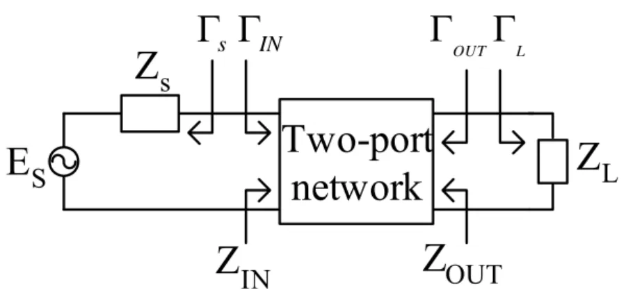
The stability of an amplifier is a very important consideration in a design and can be determined from the S parameters, the matching networks, and the terminations. The two-port network is shown in Figure 3-1.
E
SZ
sΓ
sΓ
INZ
INTwo-port
network
OUTΓ
LΓ
Z
OUTZ
LFigure 3-1: Stability of two-port networks.
A two-port network to be unconditionally stable can be derived from (3.1) to (3.4). Γs <1 (3.1) ΓL <1 (3.2) 1 1 22 1 2 2 1 11 − Γ < Γ + = Γ L L N I S S S S (3.3) 1 1 11 1 2 2 1 22 − Γ < Γ + = Γ S s OUT S S S S (3.4)
stable condition. The solution of (3.1) to (3.4) gives the required conditions for the two-port network to be unconditionally stable [5].
A convenient way of expressing the necessary and sufficient conditions for unconditional stability is 21 2 1 2 2 2 2 2 11 2 1 S S S S k= − − + Δ , k >1 (3.5) Δ=S11S22 −S12S21 ,Δ <1. (3.6)
3.1.2 Impedance matching
Consider the RF system shown in Figure 3-2. Here the source and load are 50Ω (a very popular impedance), as are the transmission lines leading up to the IC. For optimum power transfer, prevention of ringing and radiation, and good noise behavior, for example, we needs the circuit input and output impedances matched to the system. In general, some matching circuit must almost always be added to the circuit.
E Input matching network Input matching network ZS Input matching network ZL ZS=50Ω ZL=50Ω
Typically, reactive matching circuits are used because they are lossless and because they do not add noise to the circuit which will only be matched at a range of frequency. If a broadband matching is required, then other techniques may need to be used. Note that, in general, the impedance of a circuit is complex
(
R+ jX)
.Then, tomatch it, the matching must be driven for its complex conjugate
(
R− jX)
.A more general matching is required if the real part is not 50Ω. For example, if the real part of Z is less than 50Ω, then the circuit can be matching using the circuit in in
Figure 3-3.
L
C Matching 0 3Z
Z
=
0 3Y
Y
=
2 2or
Y
Z
Z
inor
Y
inFigure 3-3: A possible impedance-matching network.
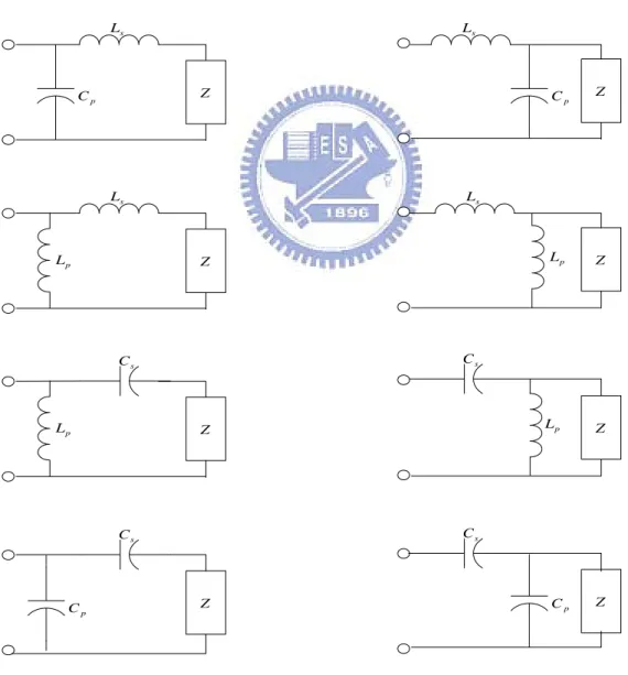
In order to the best power transfer into the circuit, it is necessary to match its input impedance to the source and the output impedance to the load. It’s very common to use reactive components to achieve this matching because they do not absorb any power or add noise. Thus, series or parallel components can be added to the circuit to provide an impedance transformation. Series components will move the impedance along a constant resistance circle on the Smith Chart: series inductor for clockwise moving and series capacitor for counterclockwise. Parallel components will move the
admittance along a constant conductance circle: parallel capacitor for clockwise moving and parallel inductor for counterclockwise moving.
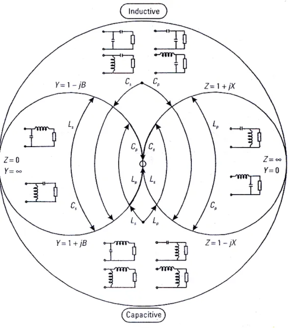
With the proper choice of two reactive components, any impedance can be moved to a desired point on the Smith Chart. There are eight possible two-components matching networks, also known as ell networks, as shown in Figure 3-4. Each will have a region in which a match is possible and a region in which a match is not possible. s L Z p C s L Z p L s C Z p L s C Z p C Z p C s L Z Z Z p C s L p L s C p L s C
In any particular region on the Smith Chart, several matching circuits will work and others will not. This is illustrated in Figure 3-5, which shows what matching networks will work in which regions. Since more than one matching network will work in any region, how does one choose? There are popular reasons for choosing one over another:
1. Sometimes matching component can be used as dc blocks (capacitors) or to provide bias currents (inductors).
2. Some circuits may result in more reasonable component values.
3. Personal preference. Not to be underestimated, sometimes when all paths look equal, you just have to shoot from the hip and pick one.
4. Stability. Since transistor gain is higher at lower frequencies, there may be a low-frequency stability problem. In such a case, sometimes a high-pass network (series capacitor, parallel inductor) at the input may be more stable. 5. Harmonic filtering can be done with a low-pass matching network (series L, parallel C). This may be important, for example, for power amplifiers. [10]
Figure 3-5: Which ell matching networks will work in which regions.
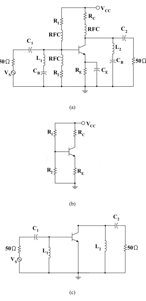
In a RF amplifier, the input and output matching networks provide the appropriate ac impedances to the transistor. The transistor must also be biased at an appropriate quiescent point. A complete RF amplifier contains both dc bias components and the ac matching network. RFCS, bypass capacitors, and coupling capacitors need to be
VS R1 RC RFC RFC RFC L1 C1 CB R 2 RE CE L2 CB 50Ω 50Ω C2 VCC (a) RE VCC RC R1 R2 (b) VS L1 C1 L2 50Ω 50Ω C2 (c)
3.1.3 Special Topic for Output: Load-line Match
Continuing with this topic from Chapter 2, we again emphasize the load-line
method because of its importance to the amplifier, especially to the PA. The method is to design the load of the power-oriented amplifiers and makes them to fit the I-V characteristic of the transistors which are the core of the amplifiers. If we operate the amplifier in the linear characteristic region of the device like the saturation region of the MOSFET, the output signal swings between Vmax and Vknee; that is, the current
varies from zero to Imax. In the V-I plot of the device, the slope of the “load line,” from
(Vmax , 0) to (Vknee , Imax), is so called Ropt. Thus, when the amplifier has its output
load which equals to Ropt, it will operate at the maximal DC variance range to deliver
the RF power.
In general, the output load of out design goal seldom equals to the Ropt of the
amplifier; hence, to design PAs, we usually adopt the matching network including the reactive device to transform Rload for Ropt, as shown in Figure 3-7.
3.2 Conventional RF power amplifier design
3.2.1 Starting at LNA
It is well-known that the LNA is the pioneer of the PA because of the ease to extend concepts parameters of LNA to PA. So studying the design of the PA, we usually pick up those of the LNA. In the design of low noise amplifier, there are many key points. These include noise figure minimization, providing sufficient gain with good linearity, reasonable power consumption, and acceptable impedance matching. It is worthy of surveying that we just need to ensure the noise level low enough, not guarantee for minimum, because the input signal level of PA is higher than that of LNA. Fig 3-8 illustrates the input stage of the low noise amplifier with source degeneration. A simple calculation is
s gs m gs s g in L C g sC L L s Z ⎟⎟ ⎠ ⎞ ⎜ ⎜ ⎝ ⎛ + + + = 2 2 2 1 ) ( . (3.7)
Choosing appropriate value of inductance and capacitance, then Lg+Ls and Cgs will
resonate at certain frequency. By choosing Ls appropriately, the real term can be made
equal to 50Ω. The gate inductance Lg is used to set the resonance frequency once Ls
is chosen to satisfy the criterion of a 50Ω input impedance. The matching method in noise performance is better than using resistance termination of the input end.
Lg
Ls ZIN
M1
M2
Fig. 3-8: Common source stage use inductance degeneration.
3.2.2 Wide-band amplifier design
For wide-band amplifier design, it’s difficult to achieve the impedance matching in wide frequency range and gain flatness in it. Again, we start this topic at the wide-band LNA topology. Figure 3-9 is the LNA circuit schematic. We discuss this circuit step by step from the first stage. First, to make1/gm = 50Ω, the gm value of
common gate amplifier is going to be fixed at certain trans-conductance. An additional stage is required to provide sufficient gain over the desired band. A shunt feedback common source amplifier is used in the second stage for this purpose. The first step is the selection of transistor size and bias condition of the M1 to yield
Ω = =1/ 50
ReZ11 gm . This ensures input matching condition for wide-band of
trade-off between noise and impedance matching in the LNA circuit. One of the major problems in the wide bandwidth amplifier design is the limitation imposed by the gain-bandwidth product of the active device. We know that any active device has a gain roll off at high frequency because of the gate-drain and gate-source capacitance in the transistor. This effect degrades the forward gain as the frequency increases and eventually the transistor stops functioning as an amplifier at the high frequency. Therefore the second design step is the selection of optimal bias point of second stage of LNA so that it operates at its maximum fT. In addition to this S21 degradation
with frequency other complications that arises in wide-bandwidth amplifier design includes, increase in reverse gain S12 and noise figure at high frequency. Negative
feedback configuration is used to reduce these effects and increase the bandwidth. An inductor L is connected in series with Rf such that after certain frequency the negative
feedback decreases in proportion to the S21 roll-off. This technique improves gain
flatness at high frequency. The load inductance of L1 and L2 replace the resistor load
which is used conventionally. The magnitude of the inductor’s impedance increases as frequency increases. This increase inductor impedance compensates the active device gain degradation that occurs at high frequency [13].
Another wide-band LNA design schematic is shown in Figure 3-10. In Figure 3-10, the Rf is added as a shunt feedback element to the conventional cascade narrow
band LNA and Lload is used as shunt peaking inductor at the output. The capacitor Cf
is used for the ac coupling purpose. The source follower, composed of M3 and M4, is
added for measurement proposes only, and provides wideband output matching. C1
and C2 are ac coupling capacitor. The small-signal equivalent circuit at he input of the
LNA is shown in Figure 3-11. The resistor RfM =Rf /(1−Av) represents the Miller equivalent input resistance of Rf, where Av is the open-loop voltage gain of the LNA.
From equivalent circuit, the value of Rf can be much larger than that of the
conventional resistance shunt-feedback. In the conventional resistance shunt-feedback, the size of Rf is limited as RfM determines the input impedance. One of the key roles of
the feedback resistor Rf is to reduce the Q-factor of the resonating narrowband LNA
input circuit. The Q-factor of the circuit shown in Figure 3-11 can be approximately given by gs fM g S T S WB
C
R
L
L
R
Q
⋅
⋅
⎥
⎥
⎦
⎤
⎢
⎢
⎣
⎡
+
+
≈
0 2 0)
(
1
ω
ω
ω
(3.8)From (3.8), and considering the inversely linear relation between the -3dB bandwidth and the Q-factor, the narrowband LNA in Figure 3-9 can be converted into a wideband amplifier by the proper selection of Rf. To design a wideband amplifier
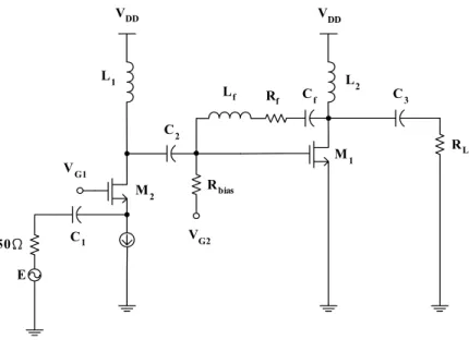
flattening the gain over a wider bandwidth of frequency with much smaller noise figure degradation [14]. E VDD VDD VG1 VG2 M2 M1 50Ω C1 C2 Cf C3 Rbias Rf Lf L1 L 2 RL
Figure 3-9: A wide-band LNA circuit schematic.
Lg C1 Rb ias Vg1 Ls Lload Rload M1 M2 M3 M4 C2 Rf Cf IN O U T VD D VD D Vg 2
s T
L
ω
Chapter4
UWB CMOS Power Amplifier design
4.1 The PA Issues of UWB Transmitter
In UWB systems, the power level from the UWB transmitter should be low enough not to interfere with the already existing communication systems, for example 802.11a. As shown in Figure 4.1[33], the low output levels that specified by the Federal Communications Commission (FCC) is less than -41.3 dBm/MHz. Therefore, for a 7 GHz bandwidth, the peak output power is approximately-3 dBm or 500μW. UWB systems need not require large transistors, and greatly lighten the difficult of CMOS technology. The main challenging task becomes to achieve a high gain and good impedance match over the entire frequency band.
Figure 4-1: The power level of UWB.
Linearity is another issue in UWB systems. For constant envelope modulation schemes like GMSK, FSK, the amplitude remains constant and non-linear high
efficiency power amplifier is used. However, non-constant envelope modulation schemes like CDMA, the amplitude of the signal also carries some data information and hence it is important to maintain the exact shape of the signal without introducing any distortion through the power amplifier. It is noted that because the bandwidth of MB-OFDM is less than DS-CDMA, the linearity requirements is more relaxed.
4.2 UWB Design for CMOS Power Amplifier
In this chapter, we introduce a two stage power amplifier for UWB application. To design a UWB PA, the first consideration is to achieve wide bandwidth matching network. At the same time, gain flatness is another important goal of the wide-band amplifier design. There are many methods for wide bandwidth matching network, such as distributed amplifier (DA) and balance amplifier etc., but we’ll provide our solution using CMOS PA design for these key points.
4.2.1 Input Matching: Cascode with Resistor Feedback
As we mentioned in Chapter 3.2, the cascade topology of resistor feedback is considered to starting my design at wide-band matching. Figure 4-2 shows the first stage of our design. The Rf is added as a shunt feedback element to the conventional
cascade narrow band amplifier and Lload is used as shunt peaking inductor at the
the impedance of the signal source. The resistor RfM =Rf /(1−Av) represents the Miller equivalent input resistance of Rf, where Av is the open-loop voltage gain of the
cascode amplifier. From its equivalent circuit, the value of Rf can be much larger than
that of the conventional resistance shunt-feedback. In the conventional resistance shunt-feedback, the size of Rf is limited as RfM determines the input impedance. One
of the key roles of the feedback resistor Rf is to reduce the Q-factor of the resonating
narrow-band amplifier input circuit. Recalling (3.7), the impedance of the amplifier with source degeneration can be derived as
s T gs s gs m gs s g in
L
sC
L
C
g
sC
L
L
s
Z
⎟
⎟
≈
+
ω
⎠
⎞
⎜
⎜
⎝
⎛
+
+
+
=
(
)
1
1
(4.1)The Q-factor of the circuit shown in Figure 4-3 can be approximately given by
gs fM g S T S WB
C
R
L
L
R
Q
⋅
⋅
⎥
⎥
⎦
⎤
⎢
⎢
⎣
⎡
+
+
≈
0 2 0)
(
1
ω
ω
ω
(4.2)From (4.2), and considering the inversely linear relation between the -3dB bandwidth and the Q-factor, the amplifier can be converted into a wideband amplifier by the proper selection of Rf. To design a wideband amplifier that covers a certain
frequency band, the amplifier will be optimized at the center frequency. The feedback resistor Rf also provides its conventional roles of flattening the gain over a wider
Figure 4-2: The input stage of our PA.
R
SL
gR
fMC
gs s TLω
L
sFigure 4-3: The small-signal equivalent circuit at the input.
4.2.2 Output Matching with Inductor-resistor Feedback
Output matching networks are also a problem to UWB PA. Since, antenna connect to the output of PA, the matching networks of PA must transfer to 50Ω for wideband application. As the components of matching network are increasing, the parasitic effects are also increasing. There come some bothering interferences such as power
loss, efficiency increase, and output noise increase.
In this work, we simplify output matching network by load-line theorem. The basic concept is selecting an optimum device it has optimum output load at 50Ω. By simulation of I-V curve, the inductor-resistor feedback topology not only benefits the goal of gain flatness but also has good performance for wideband design, as shown in Figure 4-4.
R
biasL
fR
fL
loadL
SDC blocking
R
loadM
3Figure 4-4: The output stage of our design.
Now we discuss the load-line result about this PA, as shown in Figure 4-5. In this case, the NMOS transistor of TSMC 0.18um process, has the width of160-um and the length of 0.18-um length. Lf is 2.25nH, Rbias is 350Ω, Rf is 150Ω, and Lload is 3.47nH.
When Rload is 50Ω, we set the operation point of the bias to be 1.2V of VDS and 0.8V
Figure 4-5: The I-V curve of the load-line study of the PA.
4.2.3 Gain flatness of amplifier with inductor-resistor feedback
This is the measurement of uniformity of the gain across the wide frequency range of interest. This parameter commonly used for wideband systems can impact pulse distortion in impulse-based UWB. It is desired that the gain be flat over the frequency band, typically a tolerance of ±0.5 dB.
It’s worth discussing further for the feedback of our input stage. The feedback resistor, Rf1, plays a key role for the gain as known in circuit theorems, and so do the
Lf2 and Rf2 in the output stage. The resistor feedback can be design in such a way that
it can provide the require match at both the input and output ends. Figure 4-4 show the characteristic of resistor feedback. Clearly, the low frequency gain drops due to small feedback resistor, and large feedback resistor provide good gain but have large gain variation, as shown in Figure 4-6. Since input impedance is usually on 50Ω,
m1 VDS= DC.IDS.i=0.017 VGS=0.800000 1.200 0.5 1.0 1.5 2.0 0.0 2.5 -0 10 20 30 40 50 -10 60 VGS=0.600 VGS=0.700 VGS=0.800 VGS=0.900 VGS=1.000 VGS=1.100 VGS=1.200 VDS DC .I D S .i , m A m1
small resistor can get better matching. Therefore, we might trade off between better matching and larger low frequency gain.
0.0 3.0G 6.0G 9.0G 12.0G 15.0G 0.0 2.0 4.0 6.0 8.0 10.0 12.0 14.0 16.0 Frequency(Hz) larger R feedback smaller R feedback S21(dB)
Figure 4-6: The comparison with the value of the feedback resistor.
We use inductor-resistor feedback to improve the gain at matching consideration. Inductor-resistor feedback impedance can be written as:
f f f f f
R
X
R
j
L
Z
=
+
=
+
ω
, (4.3) Analyzing with circuit theorem, the gain of the shunt-shunt feedback( )
( ) ( ) ( )
,
1
,
( )
01
+
=
−
=
==
L R i o f fI
V
j
A
Z
j
j
j
A
j
A
A
β
ω
ω
ω
β
ω
ω
(4.4) In (4.4), A( )
jω means the open-loop trans-resistance gain. According to (4.3) and(4.4), it is clear that Zf is small at low frequency and increase with the frequency raise.
Therefore, the high frequency gain can slight increase. By cascading two stages, it should get flatness over the wide bandwidth. The concept is shown at Figure 4-7.
0.0 3.0G 6.0G 9.0G 12.0G 15.0G 0 2 4 6 8 10 12 14 16 18 Frequency(Hz) CS with RL feedback sum in large-R case sum in small-R case S21(dB)
Figure 4-7: The |S21| of “common-source with RL feedback” and “two stages overall”.
4.2.4 Detail of the Power Amplifier for UWB application
We start to design a two stage power amplifier and apply Advance Design System (ADS) for simulation tools, which can supports load-pull and large signal simulation. TSMC 0.18µm process is used in this work, and small signal model and large signal model are supported by TSMC. At first, we decide the transistor parameters. We choose the width per finger is 2.5um and the finger number of each NMOS is 64; so the width of each NMOS is 160um. Besides, we add two capacitors C1 and C2 in order
to connect with the two stages: not only for inter-stage matching but also for the DC blocking purpose. After simulating, the total topology is decided as Figure 4-8 and the detail of the passive devices is listed on Table 4-1.
Device Value Device Value Rf1 400Ω Lf2 2.25nH Lg1 0.908nH Rf2 150Ω Lload1 2.45nH Lload2 3.47nH LS1 0.1nH C2 2.85pF C1 0.951pF LS2 0.15nH Rbias 350Ω
Table 4-1: Passive devices of the PA.
4.2.5 Simulation Results
To simulate the result, we apply 0.7V to VG1, 1.8V to VDD1, and 1.2V to VDD2
respectively. Figure 4-9 shows the simulated S-parameter. |S11| and |S22|are lower than
-10dB between 3.1 and 10.6GHz. And |S21| is higher than 13.5dB at the same range in
our simulation results. The -3dB bandwidth is 2.5~11.7GHz for the simulation. The noise figure (NF) of this UWB LNA is shown in Figure 4-10. The noise figure varies between 3.8 to 4.1 at 3.1~10.6GHz. Figure 4-11 shows one of the index representing the stability. This amplifier is unconditionally stable at any frequency. The two-tone test results for third-order inter-modulation distortion are shown in Figure 4-12. The test is performed at 8GHz. IIP3 is to 16.7dBm, and the input referred 1-dB compression point (ICP) is 3.98dBm. The proposed UWB PA dissipate 38.9mW with two power supplies; one is 1.8V, and the other is 1.2V. Table 4-2 represents the performance between 3.1G to 10.6GHz. B.W. (GHz) Power Gain(dB) P-1db (dBm) OIP3 (dBm) PAEmax (%) Power consumption (mW) 3.1~10.6 14.21~13.54 (15.18) 3.28~4.10 (3.99) 15.06~16.16 (16.691) 7.27~10.51 (10.79) 38.9
0.0 3.0G 6.0G 9.0G 12.0G 15.0G -25 -20 -15 -10 -5 0 5 10 15 20 Frequency(Hz)
|
S21|
|
S 11|
|
S22|
|
S|
(dB)Figure 4-9: The S-parameter of the PA.
0.0 3.0G 6.0G 9.0G 12.0G 15.0G 0 1 2 3 4 5 6 7 8 9 10 Frequency(Hz) Noise Figure
0.0 5.0G 10.0G 15.0G 20.0G 1 2 3 4 5 6 7 Frequency(Hz) Mu
4.2.6 Layout
The layout is shown in Figure 4.13, the total size occupied by the PA is 0.98x0.83 mm2, The capacitor is used metal-insulator-metal (MIM) capacitance supported by
TSMC, the models of the resistor and inductor are supplied by TSMC. The metal width is decided according to the capacity of current flow and AC signal power. Input and output pads use GSG with 50Ω, and bias-tee is used for the input end.