行政院國家科學委員會專題研究計畫 成果報告
異質整合 Mixed-signal/MEMS CMOS 無線射頻收發機設計研
發--子計畫四:可重組式 Mixed-signal/MEMS .9G~10GHz
射頻傳送端設計(2/2)
研究成果報告(完整版)
計 畫 類 別 : 整合型 計 畫 編 號 : NSC 99-2220-E-009-042- 執 行 期 間 : 99 年 08 月 01 日至 100 年 07 月 31 日 執 行 單 位 : 國立交通大學電子工程學系及電子研究所 計 畫 主 持 人 : 溫岸 計畫參與人員: 碩士班研究生-兼任助理人員:王竣傑 碩士班研究生-兼任助理人員:劉志峻 碩士班研究生-兼任助理人員:黃柏翰 碩士班研究生-兼任助理人員:林易達 報 告 附 件 : 出席國際會議研究心得報告及發表論文 處 理 方 式 : 本計畫涉及專利或其他智慧財產權,2 年後可公開查詢中 華 民 國 100 年 10 月 26 日
行政院國家科學委員會補助專題研究計畫
■成果報告
□期中進度報告
異質整合 Mixed-signal/MEMS CMOS 無線射頻收發機設計研發-
子計畫四:可重組式 Mixed-signal/MEMS .9G~10GHz 射頻傳送端設計(2/2)
計畫類別:□個別型計畫 ■整合型計畫
計畫編號:NSC 99-2220-E-009 -042 –
執行期間: 99 年 08 月 01 日至 100 年 07 月 31 日
執行機構及系所:
國立交通大學
電子工程學系及電子研究所
計畫主持人:溫瓌岸教授
計畫參與人員:
黃柏翰
,
劉志峻
,
林易達,王竣傑
成果報告類型(依經費核定清單規定繳交):□精簡報告 ■完整報告
本計畫除繳交成果報告外,另須繳交以下出國心得報告:
□赴國外出差或研習心得報告
□赴大陸地區出差或研習心得報告
■出席國際學術會議心得報告
□國際合作研究計畫國外研究報告
處理方式:
除列管計畫及下列情形者外,得立即公開查詢
■涉及專利或其他智慧財產權,□一年 ■ 二年後可公開查詢
壹、 中文摘要:
關鍵詞:極座標發射器,切換式功率放大器,MEMS 濾波器,EDA 設計流程,多模多頻帶發射機。 本子計畫目標為『Circuit/MEMS Co-design EDA 設計平台的建立以及Multiband Multimode 發射 器(Transmitter)電路設計』 由於無線通訊的蓬勃發展,具有多模的個人通訊系統需求,使得開發適用於多頻帶,並具有高線 性度及高效率的發射器成為必然的趨勢。而欲設計出.9G-10GHz 完整系統晶片,異質整合是可行的解 決方案之一,但為整合不同製程(如:MEMS,CMOS),建立一個完整的EDA 整合設計平台是必需 的。在本計畫中,會依下列流程完成包含系統架構分析、電路模組設計,並建立於可異質整合的EDA 設計環境,藉以提供傳送系統設計之整合。 依下列流程做 RF CMOS MEMS 電路開發: (1) Multiband Multimode 傳送機系統架構評估
(2) Multiband Multimode 射頻積體電路晶片及MEMS 元件設計 本計畫全程計畫為 2 年:
第一年針對.9-10GHz 傳送機系統設計所需建立之設計要項進行技術開發及環境的建立,包括: (1) Circuit/MEMS Co-design EDA 設計環境的建立
(2) Multiband Multimode 傳送機系統架構分析 (3) Multiband Multimode 傳送機系統積體電路晶片設計 由於傳送機系統中,主要電路功率放大器的特性會影響系統性能甚巨,故於第一年計畫中,故會特別 針對應用於多模多頻帶系統中的功率放大器,其非線性特性作一研究,並提出之解決方案。 第二年針對系統中可應用之 MEMS 被動元件(例如:濾波器),作一研究及設計,並利用所建立之EDA 設計環境,與電路作一整合。
貳、英文摘要:
Keywords: Polar Transmitter, Switching-Mode Power Amplifier, MEMS Filter, EDA design flow, Multi-Mode Transmitter
With development of communication market, more and more communication devices of different applications have been produced. Therefore, in transmission, a transmitter that can cover multi frequency band is also expected. To realize a .9-10GHz transmitter chipset, heterogeneous technology is a feasible solution. However, to integrate different devices (ex: MEMS, CMOS), it has to build a EDA simulation platform. In this project, the design flow includes system link budget analysis and architecture design. In addition, EDA simulation environment will be constructed for integration.
For system integration, the design targets are as follows: 1. Transmitter architecture analysis
2. Transmitter system circuit design and MEMS component development
Design target for the first year will be set on the technical development and simulation platform construction. It includes:
(1) Simulation platform construction (2) Transmitter system architecture analysis (3) Transmitter system integration
In transmission, power amplifier is the key circuit in degradations of system
performance. Therefore, the nonlinear effect of power amplifier will be research and the solution will be proposed.
Design target for the second year will be set on MEMS component design for system integration. It will primarily focus on MEMS filter design and integrate with system circuits.
參、報告內容:
近年來, 在新興消費性產品帶動、製程設計產業陸續投入 MEMS 微機電技術,以標準 CMOS 技術為平台實現感測器 SoC 化,可實現高品質,低成本之競爭優勢,Mixed-signal MEMS CMOS 儼然成為半導體產業革命性技術。Mixed-signal MEMS CMOS 實為將標準 CMOS 積體電路與 MEMS 充分整合的發展技術。而 Mixed-signal MEMS CMOS 採用現有的 標準化 IC 製程 (CMOS process)可將微電子電路以及 MEMS 微細結構以相同的設計介面整合 在一個晶片之上。為 Multi-band multi-mode (MBMO) wireless transceiver 設計, 提供了極為彈 性且頗具發展潛力的整合製作方法,台灣具備完整之半導體產業鏈,在政府持續支援之下, 應可爭取國際領先地位。 本計畫完成結合 MEMS 元件與 CMOS 電路之 RF 前端電路, 係為全球首例: (1). 可應用於極座標發射器中操作於2.5GHz/3.5GHz/5.2GHz 之E 類功率放大器, (2). 寬頻低雜訊GSM/DCS/WIMAX/WLAN之多頻帶頻率合成器 (3). 適用於多模之具備平坦雜訊表現之寬頻低雜訊放大器設計
With 0.18m CMOS implementable MEMS inductors being embedded, 63% improvements
of PA efficiency, 15.3% and 11% power saving of LNA and synthesizer can be measured. To implement compact multi-mode transceivers [1] to cover GSM/DCS/WiMAX/WiFi, the single tri-band PA with phase compensation technique [2], LNA with noise flatness using active input matching [3] and synthesizer with ripple-free scheme [4] are implemented in tsmc 0.18m CMOS (Fig.1).
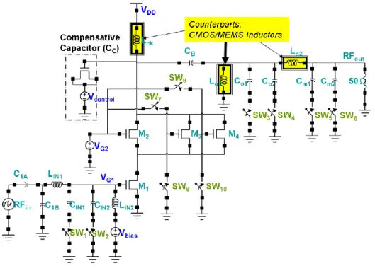
Architecture of the first tri-band cascode Class-E power amplifier operating in
2.5GHz/3.5GHz/5.2GHz frequency bands for polar transmitters is illustrated in Fig.2. The tri-band amplification is achieved by adaptation of the common-gate transistor size and the matching networks. Phase distortion from the supply modulation of the Class-E is
compensated by controlling the common-gate transistor gate voltage and a compensative capacitor. Measurement results show that the maximum power-added efficiency (PAE) of 22.7 /30.4 /29% can be obtained at 2.5/3.5/5.2GHz. Output power of 9.7/10.2/7dBm from 2.8V supply can be achieved at 2.5/3.5/5.2GHz. Gain of 9.3dB, 9.8dB and 9dB are measured at the three bands respectively. The phase distortion can be compensated from 34.4° to 3.1° under supply voltage of 0.5V to 2.8V.
Fig. 2. Schematic of the tri-band PA
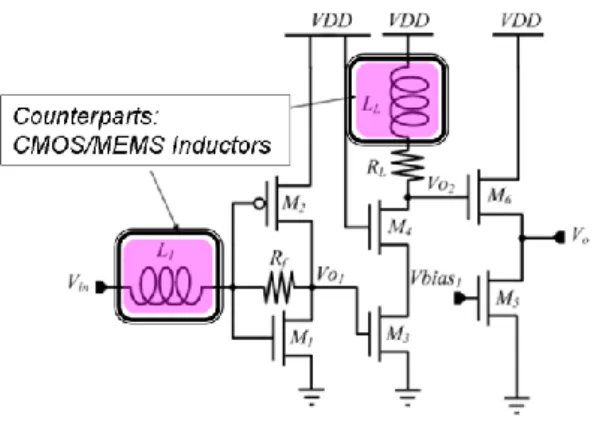
To cover 0.6 – 6GHz, a multi-stage LNA is proposed which employs input active matching technique consists of a complementary common source stage and a cascode common-source stages (Fig.3). The maximum forward power gain (S21) of 22.2dB can be achieved while drawing 17.1 mW from a 1.8-V supply. A noise figure as low as 2.85 dB and flat noise figure [5] with 2.92dB
Fig.3. Schematic of the LNA with noise flatness design
The fully integrated multi-band frequency synthesizer is designed to support IQ based GSM/DCS/WIMAX/WLAN (802.11a/b/g) transceivers (Fig.4). With ripple-free circuit, amplitude of control voltage ripple can be reduced to 3.45 μV in locking time of 13.5μs. The synthesizer performs the suppression of 31.4dB in the power spectrum of reference-spur and the peak-to-peak jitter 20.31ps. The measurement result of the QVCO in the frequency synthesizer has the phase noise performance of -123.38dBc/Hz at offset frequency 1MHz, and the FOM is -179dBc/Hz.
Fig. 4 Building blocks of the synthesizer with ripple free circuit
Monolithic integration of MEMS and ASIC can be expected with current development to adopt existing IC lines to fabricate MEMS elements [6]. With 8 inch etching tooling being installed in open CMOS foundries, MEMS inductors implementable with 0.18μm CMOS ASIC process are firstly designed and embedded in RF transceiver modules.
of dry etch are used to define and release the structure. In the first step of post processing, dielectric layers are removed by an anisotropic CHF3 /O2 reactive-ion etch (RIE) with the top metal layer acting as an etch resistant mask. After the sidewall of the microstructure is precisely defined, an isotropic SF6 /O2 RIE is performed to etch away the bulk silicon and release the MEMS structure. 3D models of MEMS 1.8nH on-chip inductors based on the etching parameters referred to the 0.18μm CMOS with post processes have been established and for quality factor analysis. Qmax of the CMOS MEMS inductor appears at 7.5GHz and with 81% incensement
from 8 to 14.5 comparing to the one implemented in CMOS process. The Qmax value is not as
superior as expected with traditional RF MEMS process with the compromise to adopt composite oxide-metal layers and restricted design rules to fit for mixed signal circuit implementations.
Two of the inductors being designed in the single LNA have been fabricated as the test keys for CMOS and MEMS counter parts analysis. Dimensions of inductor1 are selected such as 6um of
width, 2um of space, 84um of inner radius and 5.5 turns and targets to have maximum Q value at 4~5.2 GHz under CMOS design. Dimensions of inductor2 are selected such as 6um of width, 2um
of space, 75um of inner radius and 2.5 turn and targets to have maximum Q value at 2~2.4 GHz GHz under CMOS design. Counterparts with the same dimensions are fabricated with standard CMOS and post-process of substrate etching. Measurement results reveal that the Qmax of inductor1
with CMOS process appears at 5GHz as simulated by foundry provided inductor model while that of MEMS inductor shifts to 7.5GHz and the Q value increases from 8.7 to 11. Same for the MEMS inductor2 with Qmax shifts to 4GHz instead of 2GHz as designed and increases from 6.5 to 10.
Fig.5 Q factors of CMOS inductor and CMOS MEMS inductor
All the proposed single PA, LNA and synthesizer to cover wide band require high power efficiency to sustain the high linearity. The major difference of the MEMS inductor to the CMOS ones is the removal of substrate by etching processes. With the analysis of the loss caused from parasitic series resistances of inductors, quality factor dominates the loss of the circuit. Therefore, hence the MEMS inductor with higher quality factor should be able to enhance the power performances for these transceiver modules.
Some of the inductors in the proposed architectures are replaced with MEMS inductors. In the proposed multi-stage LNA, counterpart with LL and L1 in Fig.3 being replaced with MEMS
inductors are fabricated. In the tri-band PA, counterpart with Lck, Lo1, and Lo2in Fig.2 are replaced. Also, two of the inductors in QVCO in synthesizer are replaced. Improved power performance can be measured from all these counterparts and listed in Fig.6. Efficiency of the tri-band PA is with 63% improvement. Power consumption of the LNA with CMOS MEMS inductors reduces about 14% in LNA core and 16% in buffer parts and gets 14% improvement in total power consumption. Both phase noise and power consumption of the synthesizer can have 12.2% improvements. Die sizes of PA, LNA and the synthesizer are 0.24 mm2, 0.29 mm2 and 2.64 mm2 respectively. Die photos are illustrated in Fig.7-9.
System co-simulation had been done to evaluate the system performance with the proposed single PA, LNA and synthesizer. In the transmission path, relative constellation error (RCE) evaluation had been done with modulation schemes of IEEE 802.16e, 64QAM data rate and 3/4 code rate for 2.5GHz and 3.5GHz. For 5.2GHz, modulation scheme of IEEE 802.11a with 54Mbps data rate and 64-QAM is supported to polar transmission system. It reveals that the resultant RCE of -35/-31.4/-25.1dB with 5.7/6/1/8.9dB overdesign based on the spec. can be achieved at
2.5/3.5/5.2GHz respectively. For receiving path, RF/Baseband co-simulations are conducted at 2.6GHz with 64QAM, at 3.407GHz and 5.8GHz with WiMAX and at 5.2GHz with IEEE802.11a. The EVM simulated at 2.6GHz is about -31.4dB under signal sensitivity of -65dBm and adjacent channel rejection (ACR) of 4dB. EVM at 3.41GHz and 5.8GHz is about -32dB with the same sensitivity and ACR. All the parameters can hit system specifications.
Tru-band PA (2.5GHz/3.5GHz/5.2GHz) Improv ement CMO S Design CMOS with MEMS inductor Efficiec y/5.2G 6% 9.80% 63.3% LNA LNA core power (mW) 17.1 14.8 13.5% Buffer power (mW) 4.5 3.8 15.6% Total power (mW) 21.6 18.6 14% QVCO Phase noise @1MHz -123. 38dBc -125.85dBc 12.2%
Fig.7. Die photo of the counterparts of the tri-band PA.
Fig.8. Die photo of the counterparts of the LAN.
Extra Figures:
Fig.S1 Performance comparison of the tri-band PA
Fig.S3 Performance comparison of the proposed synthesizer
四、參考文獻
[1] Lee, C.P.; Behzad, A.; Marholev, B.; Magoon, V.; Bhatti, I.; Li, D.; Bothra, S.; Afsahi, A.; Ojo, D.; Roufoogaran, R.; Li, T.; Yuyu Chang; Rao, K.R.; Au, S.; Seetharam, P.; Carter, K.; Rael, J.; Macintosh, M.; Lee, B.; Rofougaran, M.; Rofougaran, R.; Hadji-Abdolhamid, A.; Nariman, M.; Khorram, S.; Anand, S.; Chien, E.; Wu, S.; Barrett, C.; Lijun Zhang; Zolfaghari, A.; Darabi, H.; Sarfaraz, A.; Ibrahim, B.; Gonikberg, M.; Forbes, M.; Fraser, C.; Gutierrez, L.; Gonikberg, Y.; Hafizi, M.; Mak, S.; Castaneda, J.; Kim, K.; Zhenhua Liu; Bouras, S.; Chien, K.;
Chandrasekhar, V.; Chang, P.; Li, E.; Zhimin Zhao; “A multistandard, multiband SoC with integrated BT, FM, WLAN radios and integrated power amplifier”
Solid-State Circuits Conference Digest of Technical Papers (ISSCC), 2010 Page(s): 454 - 455 [2] Tenbroek, B.; Strange, J.; Nalbantis, D.; Jones, C.; Fowers, P.; Brett, S.; Beghein, C.; Beffa, F.,” Single-Chip Tri-Band WCDMA/HSDPA Transceiver without External SAW Filters and with Integrated TX Power Control”, ISSCC 2008. Digest of Technical Papers. Publication Year: 2008 , Page(s): 202 – 607.
[3]Che-Cheng Liu, Mei-Fen Chou, Che-Sheng Chen, Wen-Shen Wuen and Kuei-Ann Wen, “A broadband low noise amplifier with ± 0.09dB noise flatness using active input matching” IEEE ECTI-CON, pp. 557 – 560, May 2010.
[4] B0-Heng Chen, Che-Sheng Chen, Mei-Fen Chou, Kuei-Ann Wen, “A Multi-band Frequency Synthesizer for GSM/DCS/WIMAX/WLAN Application with Ripple-free Circuit” ,2010 IEEE International Conference on Signals and Electronic Systems (ICSES), September 7-10, 2010, Gliwice, Poland
[5] Heng Zhang, Xiaohua Fan, Sinencio, E.S., “A Low-Power, Linearized, Ultra-Wideband LNA Design Technique,” IEEE J. Solid-State Circuits, vol. 44, no. 2, pp. 320 - 330, Feb. 2009. [6] Fedder, G.K.; Mukherjee, T.; “Tunable RF and analog circuits using on-chip MEMS passive components”, ISSCC 2005. Digest of Technical Papers. Publication Year: 2005 , Page(s): 390 - 391 Vol. 1.
[7] M. Talonen et al., “System requirements for OFDM polar transmitter,” 2005 European Conf. on Circuit Theory and Design, pp. 69-72, vol. 3, 2005.
[8] M. Helfenstein and G. S. Moschytz (Eds.), “Circuits and system for wireless communications,” Chapter 10, Kluwer, 2000
[9] B. Neurater et al., “GSM 900/DCS 1800 Fractional-N modulator with two-point modulation,” IEEE Microwave Symposium (MTT-S), vol. 1, pp. 125-428, 2002.
[10] Y. Huang et al., “Investigation of polar transmitters for WCDMA handset application,” The 24thNorchip Conference, pp. 155-158, Nov., 2006.
[11] P. T. M Van Zeijl et al., “A digital envelope modulation for a WLAN OFDM polar transmitter in 90nm CMOS,” IEEE JSSC, vol. 42, no. 10, pp. 2204-2211, Oct., 2007.
[12] R. B. Staszewski et al., “All-Digital PLL and transmitter for mobile phones,” IEEE JSSC, vol. 40, no. 42, pp. 2469-2482, Dec., 2005.
[13] E. Mensink et al., “Distortion cancellation by poly-phase multipath circuits,” IEEE Trans. On Circuits and System-I: Regular Papers, vol. 2, no. 9, pp. 1785-1794, Sep., 2005.
五、成果自評
本計畫完成 (1) 可應用於極座標發射器中操作於2.5GHz/3.5GHz/5.2GHz 之E 類功率放大器 (2) 寬頻低雜訊GSM/DCS/WIMAX/WLAN之多頻帶頻率合成器 (3) 多級式低雜訊放大器(LNA) 三頻帶E 類功率放大器使用0.18mm 製程並且藉由調整共基極電晶體和匹配電路以 達成三頻帶的操作。藉由獨特的共基極電晶體的偏壓和補償電容補償此E 類功率放大器 因為供給電壓的變動造成的相位失真。為了使此E 類功率放大器有更好的效能,本電路 中使用微機電製程將E 類放器之電感基底掏空,降低電感的基底所造成之基底損耗。量 測結果顯示:在2.8V 的供給電壓及6dBm 的輸入功率下,在3.5GHz 的頻帶有最大的汲極 效能:13.2%,輸出功率:10.3dBm。在供給電壓範圍為0.5V 到3V 範圍之間,此時之相位 失真被壓抑在6 度以內。為了驗證所提出之相位補償技術對於三頻帶E 類放大器應用於 極座標發射器中可增加調變訊號之準確度,建構了一個系統和電路的共同模擬環境。模 擬結果顯示:所提出之相位補償技術提升了發射器之RCE 值使得能符合WiMAX 和802.11 之系統規格要求。 全積體化之多頻帶頻率合成器搭配漣漪抑制電路於單一迴路,以 CMOS 0.18 微米製 程來實現。本頻率合成器是設計予 GSM/DCS/WIMAX/WLAN(802.11a/b/g)系統運用於以 IQ 相位為主體的收發機。此提出的頻率合成器搭配漣漪抑制電路可減小控制電壓漣漪的振 幅,來達到百萬分之 3.45 伏於鎖定時間 13.5 微秒。本頻率合成器相對於傳統方式設計 的頻率合成器在參考雜訊能量譜抑制 31.4dB,在峰到峰抖動方面有百分之 74 的改善量。 頻率合成器裡的四相位壓控振盪器的量測結果得到相位雜訊於偏移頻率 1MHz 處有22.2dB 的最大功率增益。可量測到 2.85dB 的最低雜訊值且在 0.6 到 4G 頻寬內平坦雜訊值在 2.92dB 具有正負 0.07dB 的變異量。在此提出應用於寬頻之平坦雜訊放大器並經由台積電 0.18-μm CMOS 製程進行電路實作,量測出整體具有 0.6-6GHz 的寬闖頻寬,並且驗證此多級 式低雜訊放大器適合應用於多模組系統。運用 HFSS 建立互補式金氧半(CMOS)微機電(MEMS) 電感的 3D 模型,與模擬其特性並實現與量測此電感來驗證 3D 模型的可信度。透過所提出的 具有平坦雜訊之放大器與雜訊抑制之放大器來討論高特性品質的互補式金氧半(CMOS)微機 電(MEMS)電感的影響。 獲刊登三篇國際期刊論文:
[1]. Po-Heng Chen; Che-Sheng Chen; Mei-Fen Chou; Kuei-Ann Wen; “A
Multi-band Frequency Synthesizer for GSM/DCS/WIMAX/WLAN Application with Ripple-free Circuit” 2010 IEEE International Conference on Signals and Electronic Systems (ICSES), Gliwice, 7-10 p169 - 172, Sept. 2010,
[2]. Che-Cheng Liu, Mei-Fen Chou, Che-Sheng Chen, Wen-An Tsou, Kuei-Ann Wen,” A Broadband Low Noise Amplifier with ± 0.09dB Noise Flatness Using Active Input Matching,” to be published in Electrical Engineering/Electronics, Computer, Telecommunications and Information Technology (ECTI) , May 2010.
[3]. Chung-Min Lai, Wen-An Tsou, Mei-Fen Chou, and Kuei-Ann Wen,”TRI-BAND CMOS CLASS-E POWER AMPLIFIER DESIGN WITH PHASE COMPENSATIONS FOR POLAR SYSTEMS,” to be published inCanadian Conference on Electrical and Computer Engineering, May 2010.
國科會補助專題研究計畫成果報告自評表
請就研究內容與原計畫相符程度、達成預期目標情況、研究成果之學術或應用價
值(簡要敘述成果所代表之意義、價值、影響或進一步發展之可能性)
、是否適
合在學術期刊發表或申請專利、主要發現或其他有關價值等,作一綜合評估。
1. 請就研究內容與原計畫相符程度、達成預期目標情況作一綜合評估
■ 達成目標
□
未達成目標(請說明,以 100 字為限)
□ 實驗失敗
□ 因故實驗中斷
□ 其他原因
說明:
2. 研究成果在學術期刊發表或申請專利等情形:
論文:
已發表 □未發表之文稿 □撰寫中 □無
專利:□已獲得 □申請中 ■無
技轉:□已技轉 □洽談中 ■無
其他:
(以 100 字為限)
3. 請依學術成就、技術創新、社會影響等方面,評估研究成果之學術或應用價
值(簡要敘述成果所代表之意義、價值、影響或進一步發展之可能性)(以
500 字為限)
近年來, 在新興消費性產品帶動、製程設計產業陸續投入MEMS 微機電技術,以標準 CMOS技術為平台實現感測器SoC 化,可實現高品質,低成本之競爭優勢,Mixed-signal MEMSCMOS 儼然成為半導體產業革命性技術。Mixed-signal MEMS CMOS 實為將標準CMOS 積體電路與MEMS 充分整合的發展技術。而Mixed-signal MEMS CMOS 採用現有的標準化 IC製程 (CMOS process)可將微電子電路以及MEMS 微細結構以相同的設計介面整合在一 個晶片之上。為Multi-band, Multi-mode (MBMO) wireless transceiver 設計, 提供了 極為彈性且頗具發展潛力的整合製作方法。本計畫配合國家計畫主題『Heterogeneous Integration for Better Life』,開發 可重組式Mixed-signal/MEMS CMOS 無線射頻收發機,從事異質SoC 整合設計研發。藉由 以Mixed-signal MEMS 製程及設計流程之引進,將為Multi-band,Multi-mode 無線射頻 收發機之設計帶來諸多創新發展方向,此係本計畫整合開發之主要原因,同時,依據現 今無線通訊應用需求,特以0.9G~10G Hz 涵概 GSM , DCS, GPS, PCS,Bluetooth, WLAN, WiMAX 及UWB 之設計為具體技術目標。
本計畫具體完成結合 MEMS 元件與 CMOS 電路之 RF 前端電路, 係為全球首例, 無論在 附件一
國科會補助計畫衍生研發成果推廣資料表
國科會補助計畫
計畫名稱:異質整合 Mixed-signal/MEMS CMOS 無線射頻收發機設 計研發-子計畫四:可重組式 Mixed-signal/MEMS .9G~10GHz 射 頻傳送端設計(2/2) 計畫主持人:溫瓌岸 計畫編號: NSC 99-2220-E-009 -042 –領域:
研發成果名稱
(中文)應用於極座標系統中具有相位補償之 互補金氧半三頻帶 E 類功率放大器設計(英文)Tri-band CMOS Class-E Power Amplifier Design with Phase Compensations for Polar Systems
成果歸屬機構
國 立 交 通 大 學發明人
(創作人)
賴崇閔/溫瓌岸技術說明
(中文)三頻帶 E 類功率放大器使用 0.18mm 製程並且藉由調整 共基極電晶體和匹配電路以達成三頻帶的操作。藉由獨特的共基 極電晶體的偏壓和補償電容補償此 E 類功率放大器因為供給電壓 的變動造成的相位失真。為了使此 E 類功率放大器有更好的效 能,本電路中使用微機電製程將 E 類放器之電感基底掏空,降低 電感的基底所造成之基底損耗。量測結果顯示:在 2.8V 的供給電 壓及 6dBm 的輸入功率下,在 3.5GHz 的頻帶有最大的汲極效 能:13.2%,輸出功率:10.3dBm。在供給電壓範圍為 0.5V 到 3V 範 圍之間,此時之相位失真被壓抑在 6 度以內。為了驗證所提出之 相位補償技術對於三頻帶 E 類放大器應用於極座標發射器中可增 加調變訊號之準確度,建構了一個系統和電路的共同模擬環境。 模擬結果顯示:所提出之相位補償技術提升了發射器之 RCE 值使 得能符合 WiMAX 和 802.11 之系統規格要求。(英文)A first fully integrated cascode Class-E power amplifier (PA) operating in 2.5GHz/3.5GHz/5.2GHz frequency bands for polar
transmitters is fabricated in 0.18mm CMOS technology. The phase distortion is compensated by controlling the common-gate transistor gate voltage and a compensative capacitor. To enhance the
performance, MEMS process is applied . Measurement results show that the maximum drain efficiency of 13.2% and output power of 10.3dBm can be achieved at the input power level of 6dBm from 2.8V supply in 3.5GHz frequency band. The phase distortion can be
compensated to 6° under supply voltage of 0.5V to 3V in 3.5GHz frequency band. A system co-simulation has been established for relative constellation error (RCE) evaluation and it reveals that the proposed compensations techniques make the RCE improve to meet the requirements of WiMAX and 802.11a systems in the tri-band.
產業別
IC Design技術/產品應用範圍
Wireless Communications技術移轉可行性及預期
效益
Wide band and high performance circuit module國科會補助計畫
計畫名稱:異質整合 Mixed-signal/MEMS CMOS 無線射頻收發機設 計研發-子計畫四:可重組式 Mixed-signal/MEMS .9G~10GHz 射 頻傳送端設計(2/2) 計畫主持人:溫瓌岸 計畫編號: NSC 99-2220-E-009 -042 – 領域:研發成果名稱
(中文)漣波抑制電路運用於 GSM/DCS/WIMAX/WLAN 之多頻帶頻率合成器(英文)A Multi-band Frequency Synthesizer for GSM/DCS/WIMAX/WLAN Applications with
Ripple-free Circuit
成果歸屬機構
國 立 交 通 大 學發明人
(創作人)
陳柏亨/溫瓌岸技術說明
(中文) 本成果提出一全積體化之多頻帶頻率合成器搭配漣漪抑制電路於 單一迴路,以 CMOS 0.18 微米製程來實現。本頻率合成器是設計 予 GSM/DCS/WIMAX/WLAN(802.11a/b/g)系統運用於以 IQ 相位為主 體的收發機。此提出的頻率合成器搭配漣漪抑制電路可減小控制 電壓漣漪的振幅,來達到百萬分之 3.45 伏於鎖定時間 13.5 微秒。 本頻率合成器相對於傳統方式設計的頻率合成器在參考雜訊能量 譜抑制 31.4dB,在峰到峰抖動方面有百分之 74 的改善量。頻率合 成器裡的四相位壓控振盪器的量測結果得到相位雜訊於偏移頻率 1MHz 處有-123.38dBc/Hz,其 FOM 為-179dBc/Hz。(英文)A fully integrated multi-band frequency synthesizer
implemented in CMOS 0.18μm process with the ripple-free circuit in a single loop is presented in this thesis. The synthesizer is designed for GSM/DCS/WIMAX/WLAN (802.11a/b/g) systems applying to IQ phase based transceivers. The proposed synthesizer with ripple-free circuit can reduce the amplitude of control voltage ripple to 3.45 μ V in locking time of 13.5μs. The synthesizer performs the suppression of 31.4dB in the power spectrum of reference-spur and the peak-to-peak jitter with 74% improvement compared to conventional single loop synthesizer designs. The measurement result of the QVCO in the frequency synthesizer has the phase noise performance of
-123.38dBc/Hz at offset frequency 1MHz, and the FOM is -179dBc/Hz.
產業別
IC Design技術/產品應用範圍
Wireless Communications技術移轉可行性及預期
國科會補助計畫
計畫名稱:異質整合 Mixed-signal/MEMS CMOS 無線射頻收發機設 計研發-子計畫四:可重組式 Mixed-signal/MEMS .9G~10GHz 射 頻傳送端設計(2/2) 計畫主持人:溫瓌岸 計畫編號: NSC 99-2220-E-009 -042 – 領域:研發成果名稱
(中文)適用於多模之具備平坦雜訊表現 之寬頻低雜訊放大器設計(英文)A Wideband LNA with Noise Flatness Using Active Input Matching for Multi-Band Applications
成果歸屬機構
國 立 交 通 大 學發明人
(創作人)
劉哲誠/溫瓌岸技術說明
(中文) 針對多模組應用提出使用主動輸入匹配具有平坦雜訊表現之寬頻 互補式金氧半(CMOS)低雜訊放大器之設計。本文提出之多級式低 雜訊放大器(LNA)包含互補式放大器與共射級放大器架構,並採用 主動輸入匹配方法,以達成平坦雜訊和超寬頻之設計目標。在 1.8 伏的電源供應下消耗 17.1 毫瓦可達到 22.2dB 的最大功率增益。可 量測到 2.85dB 的最低雜訊值且在 0.6 到 4G 頻寬內平坦雜訊值在 2.92dB 具有正負 0.07dB 的變異量。在此提出應用於寬頻之平坦雜 訊放大器並經由台積電 0.18-μm CMOS 製程進行電路實作,量測 出整體具有 0.6-6GHz 的寬闖頻寬,並且驗證此多級式低雜訊放大 器適合應用於多模組系統。運用 HFSS 建立互補式金氧半(CMOS) 微機電(MEMS)電感的 3D 模型,與模擬其特性並實現與量測此電 感來驗證 3D 模型的可信度。在此論文透過所提出的具有平坦雜訊 之放大器與雜訊抑制之放大器來討論高特性品質的互補式金氧半 (CMOS)微機電(MEMS)電感的影響。(英文)A flatness noise design of a wideband low noise amplifier for multi-band applications using the active input matching is proposed in this thesis. To achieve flatness noise figure and wide operating
bandwidth, the proposed multi-stage LNA employing input active matching technique consists of a complementary common source stage and a cascode common-source stages. The maximum forward power gain (S21) of 22.2dB can be achieved while drawing 17.1 mW
from a 1.8-V supply. A noise figure as low as 2.85 dB and 2.92dB flat noise figure with ±0.07dB variation from 0.6-4GHz have been
measured. Design optimization for the flat noise figure amplifiers in wide bandwidth applications is also presented and circuit
implementation in tsmc 0.18-μm CMOS process shows a 0.6-6GHz bandwidth. The novel topology of multi-stage LNA is applied for the multi-band applications. The proposed low noise amplifier was
verified by a RF/Baseband co-simulation. CMOS MEMS inductors are also imported into the proposed low noise amplifier and an amplifier with noise cancellation. 3D model of the CMOS MEMS inductors has been developed and simulated by HFSS and the test-key inductors have been measured to verify the reliability of HFSS 3D model. In this work, the effect of high quality factor of CMOS MEMS inductors will be discussed for the proposed low noise amplifier and an amplifier with noise cancellation.
產業別
IC Design技術/產品應用範圍
Wireless Communications技術移轉可行性及預期
國科會補助專題研究計畫項下出席國際學術會議心得報告
100 年 5 月 23 日 報告人 姓名 王俊凱 服務機構 及職稱 交通大學電子工程所 碩士生 會議 時間 地點 2011 年 5 月 15 日~5 月 18 日 巴西里約熱內盧 本會核定 補助文號 NSC 99-2220-E-009 -042- 會議 名稱 (中文) 2011 年 IEEE 國際電路與系統研討會(英文) 2011 IEEE International Symposium on Circuits and Systems 發表
論文 題目
(中文)單晶片含截波相關雙重取樣讀出電路之互補金氧半導體微電子機械系統 加速度計
(英文) A Monolithic CMOS MEMS Accelerometer with Chopper Correlated Double Sampling Readout Circuit
一、參加會議經過
今年 (2011) 的 IEEE 國際電路與系統研討會議 (IEEE International Symposium on Circuits and Systems) 在巴西里約熱內盧舉行。IEEE International Symposium on Circuits and Systems 多年來為 推動電路與系統技術的重要國際研討會。今年會議全程 四天,論文部分包含了十八項主題,其範 圍涵蓋相當廣泛,類比訊號處理,生醫電路與系統,通訊電路與系統,至超大型積體電路系統與 應用等等,與電路相關的主題都會被包含。 由行政院國家科學委員會補助出國會議,得以有機會參加這個國際會議。這四天中,於星期 日(15/Mar/2011) 提供一全天的短期課程(Tutorial),若要參與課程則需而外收取費用,礙於經費問 題,無參與課程訓練。星期一(16/Mar/2011)下午抵達會場註冊,星期二(17/Mar/2011)上午聽取演講, 下午聽取他人的論文發表。參加此次會議的主要目的,旨在發表一篇論文,發表時間為星期三 (17/Mar/2011)上午十點三十分。此篇論文 (Paper#1439 “A Monolithic CMOS MEMS Accelerometer with Chopper Correlated Double Sampling Readout Circuit”為口頭演說論文,聽眾反應相當良好,並 清楚的回答了三個問題。 二、與會心得 本次研討會個人認為較值得注意的重點如下: (1) 由微軟傑出工程師首席學家 Rico Malvar 的演說中提到,資訊計算與娛樂技術將改變我們的生 活,在大量的資訊中,特別是在這資訊爆炸的時代,如何有效的計算出所需要的資訊,不僅僅 是文字上的搜索,還包含圖形上的搜索,利用計算的力量來達成各種可能性。而在娛樂技術上, 過去以來無線遙控已經大幅的運用,現行最為熱門的則是感測系統,利用影像捕捉技術,以及 動態感應器來捕捉人體活動的訊號,在未來會變得更為精密,越貼近人體實際活動的情形,微 軟研究大幅展現了他們超前的研究成果。 附件三
(2) 此會議探討的研究領域甚廣,與會人士層面廣泛,有訊號處理技術、無線處理技術、介面電路 以及通訊網路等相關領域,且一時間內皆有許多場次同步進行,故會議內容非常紮實而豐富, 而會議的趨勢相會更著重在人的生活應用面。 三、考察參觀活動(無是項活動者省略) 無是項活動。 四、建議
IEEE International Symposium on Circuits and Systems 自 1993 年開始舉辦自今,為重要國際研 討會。每年研討會中並舉辦以電路與系統為主的訓練課程(Tutorial),整個研討會注重電路設計及 應用層面, 涵蓋電路技術、系統資訊、元件物理、模型建立、電路模擬、訊號處理設計、大型積 體電路設計、及無線電路設計。 行政院國科會計出國會議補助, 使交大在此重要國際會議及與學術交流的重要平台上,佔穩 一席之地。.希望國科會能繼續支持,讓國內大學的學術水準與國際能見度更上層樓。 五、攜回資料名稱及內容
(1) Proceeding of ISCAS 2011 (soft copy in flash drive) 內容為此研討會的所有論文
(2) ISCAS 2011 conference program 內容為會議議程全程資訊 六、其他
參與研討會活勳相片
相片 1: 報到註冊處 (Registration Desk)。
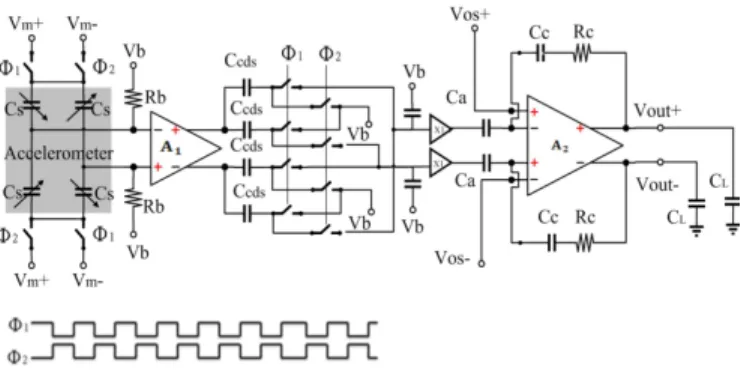
A Monolithic CMOS MEMS Accelerometer with
Chopper Correlated Double Sampling Readout Circuit
Chun-Kai Wang and Che-Sheng Chen
Department of Electronic Engineering National Chiao Tung University
Hsinchu 300, Taiwan
E-mail: [kernzip, chen.chesheng]@gmail.com
Kuei-Ann Wen
Department of Electronic Engineering National Chiao Tung University
Hsinchu 300, Taiwan E-mail: [email protected]
Abstract—A monolithic CMOS MEMS capacitive accelerometer
with micropower analog readout circuit is presented in this paper. In order to optimize noise-power performance of accelerometer in limited area, a specification driven MEMS/IC co-design flow is adopted. In analog readout circuit design, the proposed circuit architecture combines chopper stabilization and correlated double sampling to suppress low frequency noise and compensate DC offset. The RMS input referred noise voltage is 9.82 nV/√Hz under 100Hz. The power consumption is 36uW at 100kHz modulation frequency.
I. INTRODUCTION
CMOS MEMS accelerometers are applied for a wide range of applications, including automotive safety, virtual reality, movement detection, various navigation system, and mobile devices. A CMOS MEMS accelerometer has the advantages of low temperature coefficient, low power dissipation, low noise, and low cost due to it’s compatibility with wafer fabrication process. However, monolithic CMOS MEMS accelerometers fabricated with standard ASIC process have very small sensing capacitance, of which the differential relative variation usually on the order of
F
17 18~10
10− − within the bandwidth ranging from several Hz
to several hundred Hz, and that cause low mechanical sensitivity. Therefore, the main design consideration is how to suppress low frequency noise and DC offset in readout circuit design. Furthermore, for wireless devices and portable consumer electronics devices, the power dissipation is another critical design consideration for the capacitive sensing sensors.
One of the readout circuits widely used in CMOS MEMS accelerometers is switched-capacitor (SC) charge integration method [1]. The correlated double sampling (CDS) technique has been used to significantly reduce the DC offset and low frequency noise. The main drawback of the SC circuit is the related high kT/C noise with small feedback capacitor. The other one of the readout circuits is continuous-time voltage (CTV) method [2] [3]. The chopper stabilization (CS) tech-nique is employed to reduce the DC offset and low frequency noise. Both of the two noise reduce techniques could be integrated into one capacitive sensing readout circuit [4] [5]
[6]. However, the low noise readout circuits consume a power of few mW, and the low power readout interface circuits generate a noise of a few hundred μg/√Hz.
This paper presents both the readout circuit and a CMOS MEMS accelerometer. In accelerometer design, a specification driven MEMS/IC co-design flow is proposed. Low noise and compact accelerometer could be achieved. The proposed read-out circuit combines the chopper stabilization technique and the correlated double sampling to reduce low frequency noise and DC offset.
II. CIRCUIT ARCHITECTURE
The architecture of the CMOS MEMS accelerometer is shown in Fig. 1, where the fully differential capacitive bridge represents the sensing capacitors of the CMOS MEMS accelerometer. The design goal is to achieve 12-bit resolution under 1.2V peak to peak output swing with ±4g sensing range. The bandwidth of the CMOS MEMS accelerometer is up to 100Hz. At the beginning, the output noise voltage should be less than half the LSB, i.e. 14.6μV/√Hz for 100Hz bandwidth. The sensitivity could be 150mV/g due 1.2Vpp with ±4g sensing
range. Assume the voltage swing at sensor output is 1mV/g, the voltage gain readout circuit can be obtained as 44 dB.
Figure 1. Architeture diagram of the readout circuit.
Considering noise and linearity, the voltage gain of the second stage amplifier is set to be 22dB. The gain of the first
stage amplifier with the CDS circuit is 22dB. The input-referred noise is 97.3nV/√Hz. Because low noise circuit design is more easily to be achieved than MEMS design, the noise constrain of readout circuit is set to one fourth of total noise.
III. SPECIFICATION-DRIVEN MEMS/ICCO-DESIGN FLOW
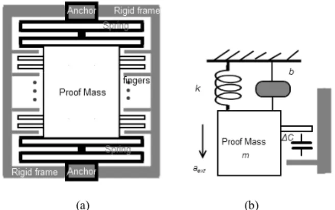
A specification-driven accelerometer design flow is proposed in this work. The target of this design flow is to find the minimum occupied area of accelerometer under required system performance. The geometry of 1-D accelerometer [7] and simplified lumped model is shown as Fig. 2. The accelero-meter could be divided into three parts: spring, sensing fingers and proof mass. In order to minimize the area of the accelero-meter, the relationship between geometry parameters and mechanical properties should be found first.
(a) (b)
Figure 2. (a)Schematic of accelerometer and (b)lumped paramter model of accelerometer
The differential equation of displacement and external acceleration of sensor is given by
ext ma kx dt dx b t d x d m 22 + + = (1)
where m is the mass of proof mass, x is the displacement of accelerometer, b is the damping coefficient and k is the stiffness of spring. With the 1st order approximation, the
equation of displacement can be simplified as
2 n ext a x ω = (2)
Based on (2), the resonant frequency ωn of sensor can be
defined by the maximum displacement at maximum sensing gravity. For example, with 4um gap process constrain, the resonate frequency is 4.98kHz with 1% displacement at 1g (g: gravity). With the maximum displacement, the maximum voltage swing at sensor output could be found as
swing of modulation signal and d is the gap between two fingers. The sensing capacitance Cs can be expressed as
d Nlt
Cs= εair/ (4)
where N is the number of fingers, l is the finger length and t is the thickness of each finger. From (3) and (4), the larger area of fingers, the higher voltage swing at sensor output node with fixed parasitic capacitor. However, CS is limited by noise
constrain of sensor. The Brownian noise of accelerometer can be expressed as m Tb k a b bwn 8 . 9 4 = (5) where kb is Boltzmann’s constant (1.38×10⁻²³ J/K), T is
temperature, b is damping factor and m is the weight in kg of proof mass. In capacitive accelerometer, squeeze film damping is the main contributor of damping factor. The squeeze film damping is shown as
3 2 . 7 ⎟ ⎠ ⎞ ⎜ ⎝ ⎛ = d t l N b μ (6)
μ (1.85×10⁻⁶N·s/m2) is the viscosity of the air under
atmospheric pressure at room temperature. From (6), we can find the damping factor is proportional to sensing capacitance with fixed thickness and gap. In order to achieve low noise performance, the sensing capacitance should be limited and the proof mass should as large as possible. However, the sensing capacitance should be large enough to meet sensitivity constrain. Therefore, the minimum occupied area could be found under these constrains. The MEMS/IC co-design flow as illustrated in Fig. 3 is adopted for accelerometer and read-out performance evaluations.
Sensitivity > 1mV/g
Brownian noise <0.75 Total noise
Circuit design Electrical noise<Total noise/4
Set Id1=1uA (WL)1=1um2 Electrical Thermal noise<Total noise/8 Yes No Id1=Id1+1
Design Gain Bandwidth Setup chopper frequency
Electrical flicker noise<Total noise/8
Get MOSs W/L ratio for readout circuit goal
Yes No
(WL)1=(WL)1L+1 Cs=1fF, set Cp~150fF
Get damping coefficient b from Cs
Proof mass m=1 nano-gram Yes No
Yes No
m=m+1
Output Cs, k and m for minimizing occupied area Cs=Cs+1
Accelerometer design ωn=√K/m=x/g where x/d =1%
System Goal: 12bit-resolution
noise coefficient which is typically ten times lower than NMOS FETs. The mean square equivalent input noise could be expressed as below f g g WL K g g WL K WL K f C f g g g g g T k V V V m m fn m m fp fp ox m m m m m b nf nT ni Δ ⎥ ⎦ ⎤ ⎢ ⎣ ⎡ + + + Δ ⎟⎟ ⎠ ⎞ ⎜⎜ ⎝ ⎛ + + ⎟⎟ ⎠ ⎞ ⎜⎜ ⎝ ⎛ ≅ + = 2 1 2 5 5 2 1 2 3 3 1 1 5 1 3 1 2 2 2 ) ( ) ( ) ( 2 1 3 2 4 2 (7)
where T is absolute temperature, W and L are the dimensions of MOSFETs, Cox is the gate capacitance per area, f is
frequency, Kfp is the PMOS flicker noise coefficient, Kfn is the
NMOS flicker noise coefficient, and gm is transconductance. From (7), the larger size of MOSFET, the lower flicker noise of MOSFET. On the other side, parasitic capacitance at input node of amplifier will be larger. However, based on (3), large parasitic capacitance will degrade the sensitivity of sensor. Another design parameter for low noise is the transcon-ductance. Large transconductance of input MOSFET will suppress noise level but also consume more current.
Figure 4. Schematic of the 1st stage amplifier.
To simplify the design flow, gm3/gm1 and gm5/gm1 are set to less than 0.1 then the noise contribution of MOSFET 3~6 could be negligible. Based on (3), Cp is set to 150fF for
acceptable CS. Because it easier to design low noise circuit
than MEMS accelerometer, the electrical noise is set to one fourth of total system noise. The size of MOSFET could be found from (7) by increasing bias current slightly until meet the noise specification. The buffer is used to drive loading capacitors of CDS circuit.
B. Chopper Stabilization Technique
The principle of chopper stabilization is illustrated in Fig. 5. The approach applies modulation to transpose the signal to the chopper frequency, while the noise is unaffected. After the second multiplier, the signal is demodulated back to the original one, and the offset and noise has been modulated to the chopper frequency. This chopping operation results in and equivalent input noise spectrum that is shown in Fig. 5, where the offset and noise signal has been shifted to the odd harmonic frequencies of the chopper frequency. A low-pass filter can be used to reduce the amplitude of the offset and noise. Therefore, if the chopper frequency is much higher than the signal bandwidth, the flicker noise will be greatly reduced with this technique.
A1 fc (A) (B) (C) (A) (B) (C)
Figure 5. Concept of chopper stabilization technique.
C. Corrected Double Sampling Technique
The correlated double sampling technique is used to subtract out error voltage with two sequential samples. The technique is illustrated in Fig. 6.
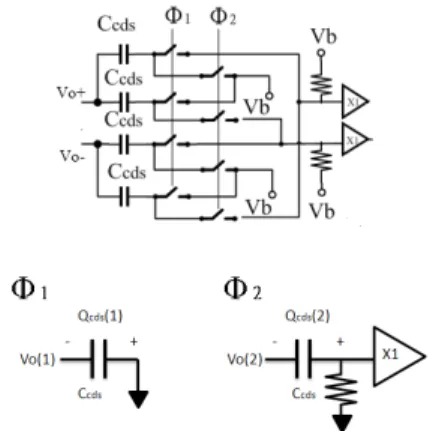
Figure 6. Schematic of correlated double sampling.
During phase one, Ccds is charged to the output. During the complementary phase, the output drives the series of the pre-charged Ccds. Due to the input chopping, the output voltage Vo is )] 1 ( ) 1 ( [ ) 1 ( 1 in error o A V V V = − + (8) )] 2 ( ) 2 ( [ ) 2 ( 1 in error o A V V V = + + (9) where Verror is the offset and the flicker noise. By inspection of Fig. 6, during Φ1, we have
cds o
cds V C
Q (1)=− (1) . (10) Therefore, duringΦ2, the voltage across Ccds becomes
in cds cds o o Ccds AV C C V V V 2 1 )] 2 ( ) 1 ( [ ) 2 ( = − + ≅ . (11) that is showing that the Verror is subtracted by CDS. The
output of the first stage amplifier is differential. Therefore, the complete scheme of the method as shown in Fig. 6 can be realized that uses two CDS structures working on both outputs. The 2kT/C noise of the output sampling is negligible compared to the input divided by 2
1
D. Second Stage Amplifier
The second stage amplifier is the folded cascade amplifier as shown in Fig. 7. An input with PMOS FETs is used due to lower flicker noise coefficient. The differential offset inputs are designed for compensating the sensor structure mismatch. Large capacitance can reduce the unit gain frequency and increase the phase margin. For the circuit architecture, the close loop amplifier of the second stage amplifier could be used as a low pass filter to remove the modulated noise signal. The second stage amplifier offers the gain of Ca/Cc.
Vdd Vdd Vb1 Vcmfb Vin+ Vin-Vout+ Vb2 Vb3 Vout-Vos+ Vos-3:1 1:3
Figure 7. Schematic of folded cascode amplifier.
V. SIMULATION RESULTS
The proposed readout circuit and CMOS MEMS accelero-meter is implemented by TSMC 1P6M 0.18um CMOS mix-signal technology. The readout circuit operates with supply voltage 1.8V. The circuit is simulated in Cadence design environment using Spectre simulator. The chopper frequency is 100kHz. The designed open loop gain of the second stage amplifier is 70.75dB. It achieves a 129Hz unit gain band-width with a 88° phase margin at a 10nF load. The input signal of readout circuit is ±4mV with ±4g sensing voltage. The noise simulation is achieved by periodic noise analysis with Spectre. The output square noise power after the CDS of the first stage amplifier is shown in Fig. 8.
Figure 8. Simulated output square noise power
Rooting the integration the square noise power from 1Hz
TABLE I. SUMMARY OF ACCELEROMETER SPECIFICATIONS
System specifications Resolution 12bit Output swing 1.2V Sensing range ±4g Accelerometer specifications Sensing Cs 4×30fF Resonant frequency 4.98kHz Mechanical noise 20.65μg/√Hz
Area (without/with rigid frame) 600um×470um / 700um×570um
Circuit specifications
DC gain 44dB Input-referrd noise 9.82 nV/√Hz Power 36uW
VI. CONCLUTIONS
The proposed circuit provides an effective solution to micropower low noise CMOS readout circuit. The CS and CDS technique is realized to reduce the offset voltage and flicker noise. The simulation results show the input-referred noise is 9.82nV/√Hz for 100Hz bandwidth and the power dissipation is 36uW. The circuit is useful due to the low noise and low power consumption. The MEMS/IC co-design flow of CMOS MEMS accelerometers provides effective system evaluation for monolithic CMOS MEMS accelerometer with readout circuit design.
ACKNOWLEDGMENT
The authors would like to acknowledge fabrication support provided by National Chip Implementation Center (CIC) and National Center of High-performance Computing for computer time and facilities. This work was conducted by Trans.-Wireless Technology Laboratory (TWT Lab.), Hsin-chu, Taiwan and sponsored by the National Science Council, Taiwan under the contract: NSC99-2220-E-009-042.
REFERENCES
[1] B. V. Amini,R. Abdolvand, and F. Ayazi, "A 4.5-mW closed-loop Delta Sigma micro-gravity CMOS SOI accelerometer," Ieee Journal of
Solid-State Circuits, vol. 41, pp. 2983-2991, Dec 2006.
[2] J. F. Wu,G. K. Fedder, and L. R. Garley, "A low-noise low-offset capacitive sensing amplifier for a 50-mu g/root Hz monolithic CMOS MEMS accelerometer," Ieee Journal of Solid-State Circuits, vol. 39, pp. 722-730, May 2004.
[3] H. W. Qu, D.Y. Fong, and H. K. Xie, "A Monolithic CMOS-MEMS 3-Axis Accelerometer With a Low-Noise, Low-Power Dual-Chopper Amplifier," Ieee Sensors Journal, vol. 8, pp. 1511-1518, Sep-Oct 2008. [4] M. Paavola, et al., "A micropower interface ASIC for a capacitive 3-axis micro-accelerometer," Ieee Journal of Solid-State Circuits, vol. 42, pp. 2651-2665, Dec 2007.
[5] M. Paavola, et al., "A Micropower Delta Sigma-Based Interface ASIC for a Capacitive 3-Axis Micro-Accelerometer," Ieee Journal of
國科會補助專題研究計畫項下出席國際學術會議心得報告
100 年 5 月 23 日 報告人 姓名 王俊凱 服務機構 及職稱 交通大學電子工程所 碩士生 會議 時間 地點 2011 年 5 月 15 日~5 月 18 日 巴西里約熱內盧 本會核定 補助文號 NSC 99-2220-E-009 -042- 會議 名稱 (中文) 2011 年 IEEE 國際電路與系統研討會(英文) 2011 IEEE International Symposium on Circuits and Systems 發表
論文 題目
(中文)單晶片含截波相關雙重取樣讀出電路之互補金氧半導體微電子機械系統 加速度計
(英文) A Monolithic CMOS MEMS Accelerometer with Chopper Correlated Double Sampling Readout Circuit
一、參加會議經過
今年 (2011) 的 IEEE 國際電路與系統研討會議 (IEEE International Symposium on Circuits and Systems) 在巴西里約熱內盧舉行。IEEE International Symposium on Circuits and Systems 多年來為推動電路與系統技術的重要國際研討會。今年會議全程 四天,論 文部分包含了十八項主題,其範圍涵蓋相當廣泛,類比訊號處理,生醫電路與系統,通 訊電路與系統,至超大型積體電路系統與應用等等,與電路相關的主題都會被包含。 由行政院國家科學委員會補助出國會議,得以有機會參加這個國際會議。這四天中, 於星期日(15/Mar/2011) 提供一全天的短期課程(Tutorial),若要參與課程則需而外收取費 用,礙於經費問題,無參與課程訓練。星期一(16/Mar/2011)下午抵達會場註冊,星期二 (17/Mar/2011)上午聽取演講,下午聽取他人的論文發表。參加此次會議的主要目的,旨 在 發 表 一 篇 論 文 , 發 表 時 間 為 星 期 三 (17/Mar/2011) 上 午 十 點 三 十 分 。 此 篇 論 文 (Paper#1439 “A Monolithic CMOS MEMS Accelerometer with Chopper Correlated Double Sampling Readout Circuit”為口頭演說論文,聽眾反應相當良好,並清楚的回答了三個問 題。 二、與會心得 本次研討會個人認為較值得注意的重點如下: (1) 由微軟傑出工程師首席學家 Rico Malvar 的演說中提到,資訊計算與娛樂技術將改變 我們的生活,在大量的資訊中,特別是在這資訊爆炸的時代,如何有效的計算出所需 要的資訊,不僅僅是文字上的搜索,還包含圖形上的搜索,利用計算的力量來達成各 種可能性。而在娛樂技術上,過去以來無線遙控已經大幅的運用,現行最為熱門的則 是感測系統,利用影像捕捉技術,以及動態感應器來捕捉人體活動的訊號,在未來會 變得更為精密,越貼近人體實際活動的情形,微軟研究大幅展現了他們超前的研究成 果。 (2) 此會議探討的研究領域甚廣,與會人士層面廣泛,有訊號處理技術、無線處理技術、
介面電路以及通訊網路等相關領域,且一時間內皆有許多場次同步進行,故會議內容 非常紮實而豐富,而會議的趨勢相會更著重在人的生活應用面。
三、考察參觀活動(無是項活動者省略) 無是項活動。
四、建議
IEEE International Symposium on Circuits and Systems 自 1993 年開始舉辦自今,為重 要國際研討會。每年研討會中並舉辦以電路與系統為主的訓練課程(Tutorial),整個研討 會注重電路設計及應用層面, 涵蓋電路技術、系統資訊、元件物理、模型建立、電路模 擬、訊號處理設計、大型積體電路設計、及無線電路設計。 行政院國科會計出國會議補助, 使交大在此重要國際會議及與學術交流的重要平台 上,佔穩一席之地。.希望國科會能繼續支持,讓國內大學的學術水準與國際能見度更上 層樓。 五、攜回資料名稱及內容
(1) Proceeding of ISCAS 2011 (soft copy in flash drive) 內容為此研討會的所有論文
(2) ISCAS 2011 conference program 內容為會議議程全程資訊 六、其他
參與研討會活勳相片
相片 1: 報到註冊處 (Registration Desk)。
國科會補助計畫衍生研發成果推廣資料表
日期:2011/10/26國科會補助計畫
計畫名稱: 子計畫四:可重組式 Mixed-signal/MEMS .9G~10GHz射頻傳送端設計(2/2) 計畫主持人: 溫瓌岸 計畫編號: 99-2220-E-009-042- 學門領域: 晶片科技計畫--整合型學術研究 計畫研發成果名稱
(中文) 應用於極座標系統中具有相位補償之(英文) Tri-band CMOS Class-E Power Amplifier Design with Phase Compensations for Polar Systems
成果歸屬機構
國立交通大學發明人
(創作人)
溫瓌岸,賴崇閔技術說明
(中文) 三頻帶E 類功率放大器使用0.18mm 製程並且藉由調整共基極電晶體和匹配電路 以達成三頻帶的操作。藉由獨特的共基極電晶體的偏壓和補償電容補償此E 類功 率放大器因為供給電壓的變動造成的相位失真。為了使此E 類功率放大器有更好 的效能,本電路中使用微機電製程將E 類放器之電感基底掏空,降低電感的基底 所造成之基底損耗。量測結果顯示:在2.8V 的供給電壓及6dBm 的輸入功率下, 在3.5GHz 的頻帶有最大的汲極效能:13.2%,輸出功率:10.3dBm。在供給電壓範 圍為0.5V 到3V 範圍之間,此時之相位失真被壓抑在6 度以內。為了驗證所提出 之相位補償技術對於三頻帶E 類放大器應用於極座標發射器中可增加調變訊號之 準確度,建構了一個系統和電路的共同模擬環境。模擬結果顯示:所提出之相位 補償技術提升了發射器之RCE 值使得能符合WiMAX 和802.11 之系統規格要求。 (英文) A first fully integrated cascode Class-E power amplifier (PA) operating in2.5GHz/3.5GHz/5.2GHz frequency bands for polar transmitters is fabricated in 0.18mm CMOS technology. The phase distortion is compensated by controlling the common-gate transistor gate voltage and a compensative capacitor. To enhance the performance, MEMS process is applied . Measurement results show that the maximum drain efficiency of 13.2% and output power of 10.3dBm can be achieved at the input power level of 6dBm from 2.8V supply in 3.5GHz frequency band. The phase distortion can be compensated to 6° under supply voltage of 0.5V to 3V in 3.5GHz frequency band. A system
co-simulation has been established for relative constellation error (RCE) evaluation and it reveals that the proposed compensations techniques make the RCE improve to meet the requirements of WiMAX and 802.11a systems in the tri-band.
產業別
其他工業製品製造業技術/產品應用範圍
Wireless Communications技術移轉可行性及
預期效益
Wide band and high performance circuit module
99 年度專題研究計畫研究成果彙整表
計畫主持人:溫岸 計畫編號: 99-2220-E-009-042-計畫名稱:異質整合 Mixed-signal/MEMS CMOS 無線射頻收發機設計研發--子計畫四:可重組式 Mixed-signal/MEMS .9G~10GHz 射頻傳送端設計(2/2) 量化 成果項目 實際已達成 數(被接受 或已發表) 預期總達成 數(含實際已 達成數) 本計畫實 際貢獻百 分比 單位 備 註 ( 質 化 說 明:如 數 個 計 畫 共 同 成 果、成 果 列 為 該 期 刊 之 封 面 故 事 ... 等) 期刊論文 0 0 100% 研究報告/技術報告 0 0 100% 研討會論文 0 0 100% 篇 論文著作 專書 0 0 100% 申請中件數 0 0 100% 專利 已獲得件數 0 0 100% 件 件數 0 0 100% 件 技術移轉 權利金 0 0 100% 千元 碩士生 4 4 100% 博士生 0 0 100% 博士後研究員 0 0 100% 國內 參與計畫人力 (本國籍) 專任助理 0 0 100% 人次 期刊論文 3 3 100% 請 詳 分 項 計 畫 報 告。 研究報告/技術報告 0 0 100% 研討會論文 1 1 100% 篇 請 詳 分 項 計 畫 報 告。 論文著作 專書 0 0 100% 章/本 申請中件數 0 0 100% 專利 已獲得件數 0 0 100% 件 件數 0 0 100% 件 技術移轉 權利金 0 0 100% 千元 碩士生 0 0 100% 博士生 0 0 100% 博士後研究員 0 0 100% 國外 參與計畫人力 (外國籍) 專任助理 0 0 100% 人次其他成果
(
無法以量化表達之成 果如辦理學術活動、獲 得獎項、重要國際合 作、研究成果國際影響 力及其他協助產業技 術發展之具體效益事 項等,請以文字敘述填 列。) 無。 成果項目 量化 名稱或內容性質簡述 測驗工具(含質性與量性) 0 課程/模組 0 電腦及網路系統或工具 0 教材 0 舉辦之活動/競賽 0 研討會/工作坊 0 電子報、網站 0 科 教 處 計 畫 加 填 項 目 計畫成果推廣之參與(閱聽)人數 0國科會補助專題研究計畫成果報告自評表
請就研究內容與原計畫相符程度、達成預期目標情況、研究成果之學術或應用價
值(簡要敘述成果所代表之意義、價值、影響或進一步發展之可能性)
、是否適
合在學術期刊發表或申請專利、主要發現或其他有關價值等,作一綜合評估。
1. 請就研究內容與原計畫相符程度、達成預期目標情況作一綜合評估
■達成目標
□未達成目標(請說明,以 100 字為限)
□實驗失敗
□因故實驗中斷
□其他原因
說明:
2. 研究成果在學術期刊發表或申請專利等情形:
論文:■已發表 □未發表之文稿 □撰寫中 □無
專利:□已獲得 □申請中 ■無
技轉:□已技轉 □洽談中 ■無
其他:(以 100 字為限)
3. 請依學術成就、技術創新、社會影響等方面,評估研究成果之學術或應用價
值(簡要敘述成果所代表之意義、價值、影響或進一步發展之可能性)(以
500 字為限)
在新興消費性產品帶動、製程設計產業陸續投入 MEMS 微機電技術,以標準 CMOS 技術為平 台實現感測器 SoC 化,可實現高品質,低成本之競爭優勢,Mixed-signal MEMSCMOS 儼然 成為半導體產業革命性技術。Mixed-signal MEMS CMOS 實為將標準 CMOS 積體電路與 MEMS 充分整合的發展技術。而 Mixed-signal MEMS CMOS 採用現有的標準化 IC 製程 (CMOS process)可將微電子電路以及 MEMS 微細結構以相同的設計介面整合在一個晶片之上。為 Multi-band, Multi-mode (MBMO) wireless transceiver 設計, 提供了極為彈性且頗具 發展潛力的整合製作方法。本計畫配合國家計畫主題『Heterogeneous Integration for Better Life』,開發可重組
式 Mixed-signal/MEMS CMOS 無線射頻收發機,從事異質 SoC 整合設計研發。藉由以 Mixed-signal MEMS 製程及設計流程之引進,將為 Multi-band,Multi-mode 無線射頻收發 機之設計帶來諸多創新發展方向,此係本計畫整合開發之主要原因,同時,依據現今無線 通訊應用需求,特以 0.9G~10G Hz 涵概 GSM , DCS, GPS, PCS,Bluetooth, WLAN, WiMAX 及 UWB 之設計為具體技術目標。