國 立 交 通 大 學
電機與控制工程學系
博士論文
新型式單相單級交流轉直流且具有輸入電流修飾的
電源轉換器
Novel Single-Phase Single-Stage AC/DC Converters
with Input Current Shaper
研 究 生: 劉興富
指導教授: 張隆國 博士
新型式單相單級交流轉直流且具有輸入電流修飾的
電源轉換器
Novel Single-Phase Single-Stage AC/DC Converters with Input Current Shaper
研 究 生: 劉興富 Student: Hsing-Fu Liu
指導教授: 張隆國 博士 Advisor: Lon-Kou Chang
國立交通大學
電機與控制工程學系
博士論文
A Thesis
Submitted to Department of Electrical and Control Engineering
College of Electrical Engineering and Computer Science
National Chiao Tung University
In partial Fulfillment of the Requirements
For the Degree of
Doctor of Philosophy
In
Electrical and Control Engineering
April 2005
Hsingchu, Taiwan, Republic of China
中 華 民 國 九十四 年 四 月
博碩士論文授權書
本授權書所授權之論文為本人在_國立交通_大學(學院)_電機與控制工程_系所 _電機電力__組__93___學年度第_2__學期取得_博_士學位之論文。 論文名稱:新型式單相單級交流轉直流且具有輸入電流修飾的電源轉換器___ 指導教授:_張隆國__________________________ 1. □同意 □不同意 本人具有著作財產權之上列論文全文(含摘要)資料,授予行政院國家科學委員會科學 技術資料中心(或改制後之機構),得不限地域、時間與次數以微縮、光碟或數位化等 各種方式重製後散布發行或上載網路。 本論文為本人向經濟部智慧財產局申請專利(未申請者本條款請不予理會)的附件之 一,申請文號為:______________,註明文號者請將全文資料延後半年再公開。 2.□同意 □不同意 本人具有著作財產權之上列論文全文(含摘要)資料,授予教育部指定送繳之圖書館及 國立交通大學圖書館,基於推動讀者間「資源共享、互惠合作」之理念,與回饋社 會及學術研究之目的,教育部指定送繳之圖書館及國立交通大學圖書館得以紙本收 錄、重製與利用;於著作權法合理使用範圍內,不限地域與時間,讀者得進行閱覽 或列印。 本論文為本人向經濟部智慧財產局申請專利(未申請者本條款請不予理會)的附件之 一,申請文號為:______________,註明文號者請將全文資料延後半年再公開。 3.□同意 □不同意 本人具有著作財產權之上列論文全文(含摘要),授予國立交通大學與台灣聯合大學系 統圖書館,基於推動讀者間「資源共享、互惠合作」之理念,與回饋社會及學術研 究之目的,國立交通大學圖書館及台灣聯合大學系統圖書館得不限地域、時間與次 數,以微縮、光碟或其他各種數位化方式將上列論文重製,並得將數位化之上列論 文及論文電子檔以上載網路方式,於著作權法合理使用範圍內,讀者得進行線上檢 索、閱覽、下載或列印。 論文全文上載網路公開之範圍及時間 – 本校及台灣聯合大學系統區域網路:94 年 12 月 1 日公開 校外網際網路:94 年 12 月 1 日公開 上述授權內容均無須訂立讓與及授權契約書。依本授權之發行權為非專屬性發行權 利。依本授權所為之收錄、重製、發行及學術研發利用均為無償。上述同意與不同 意之欄位若未鉤選,本人同意視同授權。 研究生簽名: 學號:8812804 日期:民國 94 年 6 月 1 日國家圖書館博碩士論文電子檔案上網授權書
本授權書所授權之論文為本人在_國立交通_大學(學院)_電機與控制工程_系所 _電機電力__組_93___學年度第_2_學期取得_博_士學位之論文。 論文名稱:_新型式單相單級交流轉直流且具有輸入電流修飾的電源轉換器____ 指導教授:__張隆國_________________________ □同意 □不同意 本人具有著作財產權之上列論文全文(含摘要),以非專屬、無償授權國家圖書館,不限 地域、時間與次數,以微縮、光碟或其他各種數位化方式將上列論文重製,並得將數位 化之上列論文及論文電子檔以上載網路方式,提供讀者基於個人非營利性質之線上檢 索、閱覽、下載或列印。 上述授權內容均無須訂立讓與及授權契約書。依本授權之發行權為非專屬性發行權利。 依本授權所為之收錄、重製、發行及學術研發利用均為無償。上述同意與不同意之欄位 若未鉤選,本人同意視同授權。 研究生簽名: 學號:8812804 (親筆正楷) (務必填寫) 日期:民國 94 年 6 月 1 日 1. 本授權書請以黑筆撰寫,並列印二份,其中一份影印裝訂於附錄三之一(博 碩士論文授權書)之次頁.推薦函
一、事由:推薦電機與控制工程系博士班研究生劉興富提出論文以參加國立交通大學博 士論文口試。 二、說明:本校電機與控制工程系博士班研究生劉興富已完成博士班規定之學科及論文 研究訓練。 有關學科部分,劉君已修畢應修學分(請查學籍資料,學號 8812804),通過資 格考試;有關論文方面,劉君已完成“新型式單相單級交流轉直流且具有輸入電流修飾的電源轉換器"初稿。其相關論文已刊登於IEEE Transactions on Power
Electronics, Jan./2005 和 IEEE Transactions on Industrial Electronics,
Feb./2005。同時所研發的新技術已獲得發明專利認證另有多篇論文分別發表於重 要的國內外研討會(請參閱博士論文著作目錄)。 三、總言之,劉君已具備國立交通大學電機與控制工程系博士班研究生應有之教育及訓 練水準,因此推薦劉君參加國立交通大學電機與控制工程系博士論文口試。 此致 國立交通大學電機與控制工程系 電機與控制工程系教授
國 立 交 通 大 學
論 文 口 試 委 員 會 審 定 書
本校 電機與控制工程學系 博士班
劉興富
君
所提論文:
新型式單相單級交流轉直流且具有輸入電流修飾的
電源轉換器
合於博士資格水準、業經本委員會評審認可。
中 華 民 國 九十四 年 四 月二十七 日
口試委員:
指導教授:
系 主 任:
Department of Electrical and Control Engineering National
Chiao Tung University
Hsinchu, Taiwan R.O.C.
Date: April 27, 2005
We have carefully read the dissertation entitled Novel Single-Phase
Single-Stage AC/DC Converters with Input Current Shaper submitted by
Hsing-Fu Liu in partial fulfillment of the requirements of the degree of
新型式單相單級交流轉直流且具有輸入電流修飾的
電源轉換器
學生:劉興富 指導教授
:張隆國
國立交通大學電機與控制工程學系﹙研究所﹚博士班
摘
要
本論文研製之新型輸入電流修飾器應用於交流轉直流電源轉換器,此
轉換器具有輸入電流諧波校正功能以及輸出電壓快速反應特性。在文中所
介紹的輸入電流修飾器應用在兼具電流校正功能的反馳式架構,順向式架
構和橋式架構。明顯改善了傳統交流轉直流電源轉換器中輸入電流的諧波
電流,若經過適當設計功率因數可高達
90%以上,且只要選用傳統控制器
既可完成穩定輸出電壓與電流,是一項精巧而實用的研究成果。所有文中
提及的電路都是在穩態情況作分析與考量。所做的分析研究包括操作原理
分析、重要參數分析、電路設計步驟最後還有電路模擬或雛型電路實作驗
證性能。
這論文研究的交流轉直流電源轉換器中利用變壓器加繞一線圈達到兩
個主要優點:
(i) 本設計大大減小舊有單級 Boost-型功率因數校正單元中的
大電感。 在同樣輸出瓦特數, 舊有單級具功率因數校正轉換器中的 boost
電感有高至
1.7 倍於磁化電感的感值,或是 1.4mH 的感值。在論文中所研
究的電路所使用的電感 L
1其電感值可低至
0.1 倍於磁化電感或是 30μH 的
電感值。(ii) 另一優點是在輸入端整流用的大電容電壓差可以控制在 450V
以下, 經由調整變壓器線圈的圈數比可以達成即便是在全範圍輸入電壓也
適用(90V~265V)。雖然這幾年有不少類似技術文獻的出現,其中有些要用
到較複雜的控制電路達到高的功率因數、非固定切換頻率作高功率因數調
整或是在電路前段的升壓部分仍具有大體積的電感,過去所提的這些方法
固然有其個別優點,可是在競爭激烈的切換式電源市場角度評量,電路架
構簡單、高信賴度、以及成本是主要考量因素。
本文中所新提出的轉換器即使在輸入功率高至
600W 應用範圍也能滿
足規範
IEC61000-3-2 class D 的要求,且具有輸出電壓快速動態反應的性能。
文中所研究的電路具有結構簡單,高信賴度,與低的成本。其中的切換頻
率是定頻式,對於變壓器設計和電磁干擾防治可有較好的效果。且論文中
研究的電路可以用最普通的控制器
UC3842 或 TL494 來完成應用設計而且
電氣性能表現符合電流諧波規範。
iiNovel Single-Phase Single-Stage AC/DC Converters with Input Current
Shaper
Student:Hsing-Fu Liu Advisors:Dr. Lon-Kou Chang
Department﹙Institute﹚of Electrical and Control Engineering
National Chiao Tung University
ABSTRACT
This dissertation presents a new input current shaper (ICS) for single-phase single-stage AC/DC converters with harmonic current correction and fast output
voltage regulation. The proposed ICS are applied in flyback structure, forward
structure, and bridge structure with the function of harmonic current correction. All the circuits are analyzed in steady state consideration. The study contains operation principle analysis, critical parameters analysis, design procedure. Finally, simulations and experiment results are shown for verifications.
In the proposed AC/DC converters, an extra winding wound in the transformer provides two key advantages: (i) The size of the bulk inductor used in the conventional boost-based PFC cell can be significantly reduced in the proposed converters. In same output power application, the main transformer should has similar size but the
boost inductor in prior single-stage PFC converter will be up to 1.7Lm or 1.4mH, and
the inductor L1 in the proposed circuit can be down to 0.1Lm or 30μH. (ii) The voltage
across bulk capacitor can be held under 450V by tuning the transformer windings ratio even though the converter operates in a wide range of input voltages (90V~265V/ac). Similar technique has been reported in recent years, but complex control circuit is needed to achieve high power factor or still use a bulk inductor in the boost-cell in the
front stage of the converter. In a competitive market of switching power supply, the main consideration includes a simple, reliable, and cost-effective. Therefore, there is an improved opportunity in those presented solutions.
These new converters comply with IEC 61000-3-2 class D from the load range up to 600W, and can achieve fast output voltage regulation. The proposed circuit has a simple, reliable, and cost-effective structure. The switching frequency is fixed in the proposed converters, which benefits the design of transformer and EMI filter. The proposed solution employs conventional controller, UC3842 or TL494, to implement the circuits and the solution can comply with the agent’s standards.
誌
謝
首先感謝指導老師張隆國博士五年多來在各方面的協助與指導,進博士班很重要的 是有位學風自由與術德兼備的指導老師,很榮幸我遇到了。張老師在學術研究上讓我有 很大思考空間,所以我很快的確定研究方向,同時每當我在研究上遇到困難時都能適時 協助化解疑惑讓我的研究能有所進展。而且指導過程中時常提醒我一個很重要的觀念, 學術研究只是人生中的一個小過程,重要的是人生的價值與意義一定要清楚把握,這聲 音一值盤旋在我的心裡很久。很榮幸成為張老師門下首位取得博士學位學生。 在論文寫作上除了平日指導老師的教導,非常感謝口試委員李祖添教授,陳德玉教 授,潘晴財教授,劉添華教授與廖德誠教授在百忙中提出寶貴的建議與指導讓我的論文 更為兼備與完整。 謝謝學弟晏銘協助我平日忙碌中所無法完成的事,還有 815 實驗室學弟妹們,胡致暉, 阿信,蔡銘裕,李恆毅,楊如璇,陳鵬宇,洪嘉偉,劉志偉,李奕廷,陳彥廷,黃柏蒼, 曹文昇,我感受到大家的關心與祝福,也祝福大家順利完成學業。 在求學中兼顧工作若沒有主管支持很難成就,所以非常謝謝沛亨半導體總經理李明儒 先生與昔日主管陳繼健先生; 聚積科技總經理楊立昌先生與副總吳仲佑先生,還有我的 工作夥伴們吳志鈺,李燕婷,李偉任,許紘薰,孫僅,張育倫,信華,雅燕,謝謝大家 工作上體諒與幫忙。 為了兼顧研究與工作會忽略很多家庭生活,很感恩一直陪伴我支持我的父母與妻子, 謝謝您們讓我無後顧之憂盡心完成學業,還有一直從旁協助我的姊姊們與哥哥,僅將此 小小研究成果獻給我摯愛的家人,和關心我的親戚與朋友,同時讓大家一起分享此時的 喜悅與榮耀。 劉 興 富 2005 春天 于 新竹交通大學
CONTENTS
CHINESE ABSTRACT..………..………..…………...…i ABSTRACT………..………..….….iii ACKNOWLEDGEMENT………...……….………...…..v CONTENTS………..………..….…vi LIST OF TABLES…………..………ix LIST OF FIGURES…………..…….………..…...x CHAPTER 1. INTRODUCTION ………1 1.1 Motivation………1 1.2 Literature Survey………..………..…...……21.3 Contributions of the Dissertation…….…..………..….………..5
1.4 Outline……….………6
CHAPTER 2. A SURVEY of PREVIOUS SINGLE-STAGE PFC CIRCUITS…………..7
2.1 The Familiar Single-Stage Single-Switch PFC Rectifiers……….…...7
2.2 Some Technologies for Lowering the Voltage Stress of Bulk Capacitor……..………..……….……….11
2.3 The Proposed New Design for Lowing the Voltage Stress of Bulk Capacitor………..……….13
2.4 The Design consideration for choosing DCM and/or CCM Operations…….…..………..………...15
2.5 International Standard IEC 61000-3-2………....…17
CHAPTER 3. THE FLYBACK CONVERTER USING THE PROPOSED INPUT CURRENT SHAPER.………..………..19
3.1.1 Operation Modes M1 (t0, t1) and M6 (t5, T/2)……….……..22
3.1.2 Operation Modes M2 (t1, t2) and M5 (t4, t5)………...23
3.1.3 Boundary condition between CCM and DCM………26
3.1.4 Operation modes M3 (t2, t3) and M4 (t3, t4)……….….27
3.2 Analysis of Converter Operation……….……31
3.2.1 Primary current iN1 and Duty ratio D………...31
3.2.2 Starting conduction angle……….31
3.2.3 Voltage across bulk capacitor………..32
3.2.4 Inductor L1……….….36
3.3 Design Procedure……….….36
3.4 Experimental Results………....39
3.5 Extension Circuit………...43
CHAPTER 4. THE FORWARD CONVERTER USING THE PROPOSED INPUT CURRENT SHAPER…….………..………...44
4.1 Basic Operation Theories……….…45
4.1.1 Operation Modes M1 or M4 (during t0~t1 or t3~T/2)………46
4.1.2 Operation Modes M2 or M3 (during t1~t2 or t2~t3)………...50
4.2. Analysis of Converter Operation………....53
4.2.1 Line Current and Duty Ratio………..…...53
4.2.2 Corner Angle of Line Current……….…...54
4.2.3 Voltage Across Bulk Capacitor……….……….…...55
4.2.4 Inductor L1.……….……….56
4.3 Design procedure……….…….57
4.4 Experimental Results………....58
CHAPTER 5. THE FULL-BRIDGE CONVERTER USING THE PROPOSED
INPUT CURRENT SHAPER….……….……….…...63
5.1 Basic Operation Theories……….…64
5.1.1 Operation Modes M1 or M4 (during t0~t1 or t3~T/2) …………..66
5.1.2 Operation Modes M2 or M3 (during t1~t2 or t2~t3)………..70
5.2 Analysis of Converter Operation….………...………76
5.2.1 Line Current and Duty Ratio….………76
5.2.2 Corner Angle of Line Current….………..…77
5.2.3 Voltage Across Bulk Capacitor……….………...78
5.2.4 Inductor L1. ….………..……….79
5.3 Design procedure………..…….………..82
5.4 Simulation Results………..……….83
5.5 Extension Circuits………..………..…86
CHAPTER 6. Summary and Future Research………..90
6.1 Summary……….………..……....…...90
LIST OF TABLES
Table 2.1 Limits for IEC 61000-3-2 class D equipment………..….…18
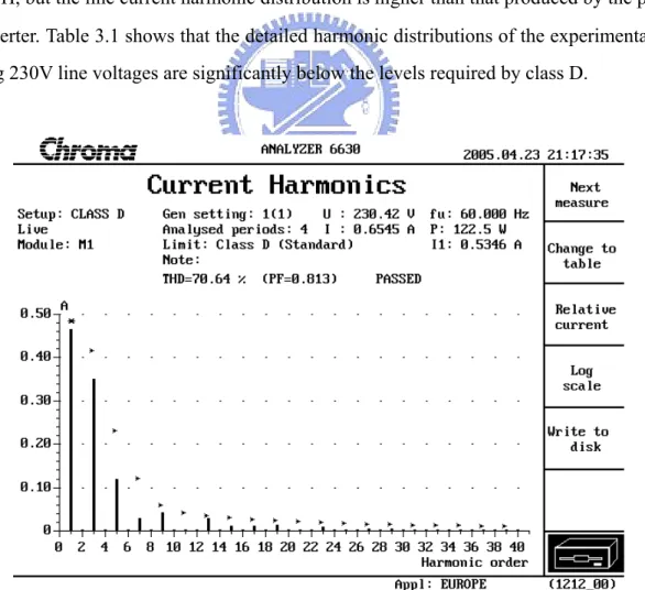
Table 3.1 The main harmonic contents of the line current, Po=48V/2A, in proposed
flyback converter……….39
Table 4.1 The main harmonic contents of the line current, Po=48V/2A, in proposed
forward converter………....60
Table 4.2 Voltage stress of S1, voltage across bulk capacitor C2 and efficiencyη…..61
Table 5.1 Harmonic main contents of the line current, Po=50V/10A, in proposed
full-bridge converter………...………84
Table 5.2 Harmonic main contents of the line current, Po=50V/10A, in proposed
half-bridge converter………..87
Table 5.3 Harmonic main contents of the line current, Po=50V/10A, in proposed
push-pull converter…...……….…………89 Table. 6.1 Comparison table between proposed circuit and prior circuits…………...91
LIST OF FIGURES
Fig. 1.1 Classical ac/dc converter with PFC function………..2
Fig. 1.2 Prior Single Stage ac/dc PFC converter…..………..3
Fig. 1.3 Proposed Single Stage ac/dc converter…...………..3
Fig. 2.1 Tree of single-stage PFC with boost-type ICS………..…7
Fig. 2.2 Structure for capacitor in series path……….…...….8
Fig. 2.3 Single-stage PFC characterized by an energy storage capacitor in the series path of the energy flow, (a) BIBRED (b) BIFRED presented in [3]…... ……..8
Fig. 2.4 The three-terminal structure for arranging the capacitor in parallel path……..9
Fig. 2.5 The ICS implemented by three-terminal structure [7], (a) circuit, (b) VCB and Vac.………...10
Fig. 2.6 The three-terminal structure for adding an extra winding in power transformer………..11
Fig. 2.7 Circuit with an extra winding in transformer………....12
Fig. 2.8Circuit with two extra windings in transformer……….…12
Fig. 2.9Circuit with magnetic switch winding in transformer……….…..12
Fig. 2.10 Circuit with magnetic switch winding in transformer ………...12
Fig. 2.11 The schematic to obtain the proposed design……….. 13
Fig. 2.12 Proposed simple flyback AC/DC converter…….………..14
Fig. 2.13Line current in DCM waveform……...……….…16
Fig.2.14Line current in CCM waveform………...……….…16
Fig. 3.1 Proposed flyback AC/DC converter with ICS.……….………....19
Fig. 3.2 Operation modes in proposed flyback converter……….…………..……….…21
Fig. 3.3 Current and Voltage waveforms in a switching cycle in M1~M3………....21
Fig. 3.4 Current loop in mode M1: (a) t0,M1< t ≤ t1,M1, S1 turns on (b) t1,M1< t ≤ t2,M1, S1 turns off………..…..…………23
Fig. 3.5 Current loop in mode M2:(a) t0,M2 < t ≤ t1,M2, S1 turns on (b) t1,M2 < t ≤ t2,M2,
S1 turns on (c) t2,M2 < t ≤ t3,M2, S1 turns off………...……...25
Fig. 3.6 Current loops in mode M3: (a) t0,M3 < t ≤ t1,M3, S1 turns on (b) t1,M3 < t ≤ t2,M3, S1 turns on (c) t2,M3 < t ≤ t3,M3, S1 turns off (d) t3,M3 < t ≤ t4,M3, S1 turns of……28
Fig. 3.7 Starting conduction angle……….………..32
Fig. 3.8 Curve of starting conduction angle, Vo/Vm, D and N1/N2 at N2/N3=2…….…..32
Fig. 3.9 Curve of starting conduction angle,VC2, and n1/n3 at Vo=48V………...33
Fig. 3.10 Max L1/LN2 and Duty cycle………...34
Fig. 3.11 Waveforms of iac&Vac at n1:n2:n3=1.2:1:0.5, L1=33μH……….34
Fig. 3.12 Waveforms of iac&Vac at n1:n2:n3=0.8:1:0.5, L1=33μH………35
Fig. 3.13 Harmonic current at n1/n2=1.2 or n1/n2=0.8.……….…….…35
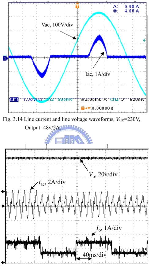
Fig. 3.14 Line current and line voltage waveforms, Vac=110V, Output=48V/2A……..40
Fig. 3.15 Dynamic response waveforms for output voltage Vo, line current iac , output current Io. Ch1->Vo, Ch2-> iac, Ch3-> Io=0.75A/1.5A……...…………..40
Fig. 3.16 Voltage rating of bulk capacitor and line voltage……….….41
Fig. 3.17 Test system picture………..……….…42
Fig. 3.18 The prototype of the proposed converter and test results at Vac=110V and 48V/2A output……..……….……….………...42
Fig. 3.19 The proposed twin transistors flyback converter………...…..43
Fig. 4.1 Proposed forward AC/DC converter with ICS……….…...44
Fig. 4.2 Operation modes in half of line cycle………...46
Fig. 4.3 Voltage and current waveforms in two modes………46
Fig. 4.4 Current loops during S1 (a) turns on (t0,M1 ≤ t < t1,M1), (b) turns off (t1,M1 ≤ t < t2,M1), (c) turns off(t2,M1 ≤ t < t3,M1) in mode M1/M4…..………...…..…48
Fig. 4.5 Current loops during S1 (a) turns on (t0,M2 ≤ t < t1,M2), (b) turns on (t1,M2 ≤ t < t2,M2), (c) turns off(t2,M2 ≤ t < t3,M2) in mode M2/M3…..……….51
Fig. 4.6 VC2 & Duty cycle, n2/n3 at Vo=48v………..………..….…....54
Fig. 4.7 Corner angle and Vo/Vm………..………….………..55
Fig. 4.8 VC2, Corner angle and n1/n2……….……….……….……55
Fig. 4.9 iac & Vac waveform at Vac=110v ,Io=1.5A………..……..…….…….59
Fig. 4.10 Dynamic response waveforms for Vac, iac, Vo and Iowhen Vac=110V, Vo=50V and Io=0.5A/1A…………..………..……….…….…59
Fig. 4.11 Voltage stress of bulk capacitor VC2 and line voltage Vac………..….….60
Fig. 4.12 The proposed twin transistors forward converter……….…...….62
Fig. 5.1 Proposed Full-bridge AC/DC converter……….….….63
Fig. 5.2 Operation modes in one half of line cycle……….………..65
Fig. 5.3 Voltage and current waveforms in two………..……...65
Fig. 5.4 Current loops while (a) S1&S2 turn on, (b) S1&S2 turn off, (c) S3&S4 turn on, and (d) S3&S4 turn off in M1/M4……….………...68
Fig. 5.5 Current loops while S1&S2 (a) turns on, (b)~(c) turns off in mode M2/M3, and S3&S4 (d) turns on, (e)~(f) turns off in mode M2/M3………...…...72
Fig. 5.6 VC2 & Duty cycle, n2/n3 at Vo=50V………..………..77
Fig. 5.7 Corner angle and Vo/Vm………..………78
Fig. 5.8 VC2, Conduction angle and n2/n1………..……….……79
Fig. 5.9 Line voltage and line current waveforms, iN1 in CCM between t2 and t3…...79
Fig. 5.10 Line voltage and line current waveforms, iN1 in DCM………..………....80
Fig. 5.11 The waveforms for VC1&|Iac|……….…………80
Fig. 5.12 The iN1 waveform & related parameters………..……...81
Fig. 5.13 iac & Vac waveform at Vac=230v ,Io=10A………..……..…84
Fig. 5.14 Dynamic response waveforms for Vac, iac, Vo………..………..85
Fig. 5.15 Voltage rating of bulk capacitor and line voltage……….……….85
Fig. 5.16 The proposed half-bridge converter……….…….……….86
Fig. 5.19 Simulation waveforms in push-pull converter……….….……….88 Fig. 6.1 The inrush current of input port while switching on input voltage in (a) con-
ventional flyback converter (b) proposed flyback converter, at Vac=110…...92
Fig. 6.2 Converter circuit selection as a function of output voltage and output
CHAPTER 1
INTRODUCTION
1.1 Motivation
A switching mode AC/DC converter can be designed to have high power transfer efficiency. This characteristic enables AC/DC converters to be used as the primary power supplies in modern electronic products, such as personal computers, computer peripherals and test instruments. Furthermore, to suppress the quantities of harmonic current emissions, the AC/DC converters must embed a function with power factor correction or harmonic current reduction.
Usually, the requirements regarding a practical AC/DC converter are expected to have high reliability and cost-effective. Many power management controllers with power factor correction function were designed in the past, but they always used two power-stages with the IC controllers each of which has at least 8 pins, for instance, LT1509/20pins, UCC38517/20pins, FAN4803/8pins, and L4981/20pins. Therefore, their application circuits are kinds of complex. Moreover, power source is usually a critical and necessary one in electronic products, and high quality power is also required too. In another viewpoint, a simple and reliable circuit structure will gain cost-effective benefit in business consideration. Thus, a simpler and reliable circuit structure appears to be an important requirement.
The requirements above may not satisfy to each other. However, there are at least four main demands when designing the converters in wide input range (90~265 Vrms): (i) the line current harmonics must satisfy agency standards, (ii) the primary side dc bus voltage should be less than 450 V/dc to reduce the size of the dc bus capacitor, (iii) the feedback control band width should cover the line frequency to minimize low frequency output ripples and advanced dynamic response, and (iv) the circuit should be simple and flexible to enhance reliability in practical applications.
1.2 Literature Survey
In recent years, many studies have presented the techniques regarding harmonic current correction in ac/dc converters. These proposed solutions could be categorized into two classes. One class yields sinusoidal input line current [1] while the other yields non-sinusoidal input line current [2], [3]. The class with sinusoidal line current has almost a unity power factor but requires a complex topology or control circuit [1], [3] and [4]. Figure 1.1 schematically shows an ac/dc converter belonging to the sinusoidal input line current class.
This kind of converters uses two power conversion stages. The first stage is used to transfer the AC power to a DC output with near unity power factor. The controllers have designed to fit the input ac current waveform to the ac voltage waveform. Under this control strategy the bandwidth of PFC is under 120Hz so dc output voltage doesn’t have good regulation [1]. Thus, an extra dc/dc converter is needed to solve the regulation problem and more cost will be required.
The other one with non-sinusoidal line current has a simple topology based on a single-stage single-switch. Although they don’t provide unity power factor in [5]-[13], they comply with IEC 61000-3-2 class D [6]. A family of such circuits was described in [5]-[13]. The family of circuits often has a common configuration, a boost circuit applied to a dc/dc converter, as shown in Fig. 1.2. This feature successfully simplifies a conventional two-power-stage with power factor corrector into a single-power-stage corrector.
This kind of the converters uses only one switch and one stage circuit. However, their topologies commonly contain two parts; those are the input current shaper [ICS] and the dc/dc
Vac Filters and Rectifier P.F.C DC/DC LOAD Vo Vac Filters and Rectifier P.F.C DC/DC LOAD Vo Vac Filters and Rectifier P.F.C DC/DC LOAD Vo Vac Filters and Rectifier P.F.C DC/DC LOAD Vo Vo Vac Filters and Rectifier P.F.C DC/DC LOAD Vo Vac Filters and Rectifier P.F.C DC/DC LOAD Vo Vo Vac Filters and Rectifier P.F.C DC/DC LOAD Vo Vac Filters and Rectifier P.F.C DC/DC LOAD Vo Vo Vo Vo
converting circuit. They are driven by one common switch. Through the switch operates the input current shaper, denoted by ICS, pulling in the input power current and the average of the current is determined by the input voltage as long as the ICS conducts. Thus, the power factor will be smaller than one but can be kept to a pretty high value if ICS is designed properly. Simultaneously, the controller in the circuit is only responsible for the dc/dc converter, and the line current is shaped by ICS. Therefore, a conventional controller can be employed in the proposed circuits.
Some interested circuits with PFC function are presented in [14]-[16]. In [14], it employs a dither signal to achieve power factor correction and it still needs a bulk inductor in PFC cell.
Filters and Rectifier Power Stage Lb Single Stage Vac LOAD Vo Filters and Rectifier Power Stage Lb Single Stage Vac LOAD Vo Filters and Rectifier Power Stage Lb Single Stage Vac LOAD Vo Filters and Rectifier Power Stage Lb Single Stage Vac LOAD Vo LOAD Vo
Fig. 1.2 Prior Single Stage ac/dc PFC converter
Filters and Rectifier Power Stage
V
ac LOADV
o Filters and Rectifier Power StageV
ac LOADV
o LOADV
o Filters and Rectifier Power StageV
ac LOADV
o LOADV
o Filters and Rectifier Power StageV
ac LOADV
o LOADV
opower efficiency with PFC converter but it needs an extra power stage to share a part of power flow. In [16], an auxiliary output of the main converter is used in parallel with the rectified input voltage instead of the series connection and the circuit also has a bulk inductor (~1mH) as the energy transfer component.
There are some papers presented about the single-phase single-stage bridge-type converters with input current shaper. A basic topology for bridge-type converter with input current shaper is presented in [17]-[18]. The circuit suffers from high voltage in dc bus
voltage when input voltage is up to 260V in heavy load and low input inductance Lin. The
circuit presented in [19] is the simplified one from [17]. It also suffers the same issue as [17]. An improved circuit for [19] is presented in [20]. The improved circuit can keep dc bus voltage under 450V in wide line and load range. In [21], it proposes a zero-voltage zero-current-switched full-bridge converter but it still suffers high voltage in dc bus voltage when input voltage is up to 260V in heavy load. A soft-switching mode rectifier (SSMR) consisting of a power factor correction zero-voltage-transition-pulse-width-modulated is presented in [22], the circuit has sinusoidal line current with low harmonics and near unity power factor via special control method. An interested regulator is realized with an asymmetrical PWM control and two coupled inductors, which can achieve ZVS and high power factor in [23]. In [24], an asymmetrical control and synchronous rectification are employed to achieve high power efficiency but a bulk inductor is still in power loop. In [25] and [26], that introduce a lot of topologies which performance can conform to IEC 61000-3-2 class D and still can’t avoid to use a bulk inductor in these circuits.
1.3 Contributions of the Dissertation
This study proposes a new converter with the configuration shown in Fig. 1.3. The new converter satisfies the input harmonic current constraints given by IEC 61000-3-2 class D and provides a fast output regulating response. A multi-winding transformer is employed in the proposed converter. This arrangement has three advantages. First, the size of the bulk inductor can be further reduced. Second, the line harmonic currents can be reduced. Third, the phase difference between the fundamental component of the line current and line voltage closely approaches zero. Furthermore, the voltage across the bulk capacitor can be arranged to a reasonable value under 450V/dc by adjusting the turn-ratio of two primary windings. Therefore, this design can adapt to large line voltage variation. Moreover, The switching frequency is fixed in the proposed converters, which benefits the design of transformer and EMI filter. Some valuable and useful EMI considerations are in [27]. The structure and operation principal of a new converter is explained in the following section, and the practical experimental results are shown in sections 3.4 and 4.4.
Based on the proposed concept of input current shaper, the thesis also proposes bridge-type circuits such as full-bridge converter with ICS, asymmetrical half-bridge converter with ICS, and push-pull converter with ICS. These extended circuits have several features described in above section.
1.4 Outline
Chapter 1 introduces the background regarding the study and indicates the practical requirements about ac/dc converter with input current harmonics correction.
Chapter 2 introduces previous studies and explains their features and defects. The survey focus on some selected typical topologies in single-phase ac/dc converter with input current harmonics correction presented in the recent ten years.
Chapter 3 introduces the flyback converter using the proposed input current shaper. The text contains circuit description, operation principle, circuit design procedure, prototype experiment results, and extension circuit in the section.
Chapter 4 depicts the forward converter using the proposed input current shaper. The text also covers several segments same as Chapter 3.
Chapter 5 depicts the full-bridge converter using the proposed input current shaper. The text also covers several segments same as Chapter 3. Besides, half-bridge converter and push-pull converter with input current shaper are simply described in the Chapter.
In Chapter 6, a summary regarding the proposed circuits is described. The purpose of this section is to provide a simple guide to select a suitable circuit in future practical application. A suggested future research about the proposed circuits is coved in this chapter.
CHAPTER 2
A SURVEY OF PREVIOUS SINGLE-STAGE PFC CIRCUITS
2.1 The Familiar Single-Stage Single-Switch PFC Rectifiers
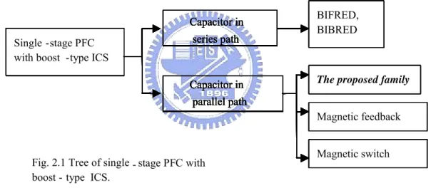
Many papers have been presented about single-stage PFC rectifiers with boost-type ICS in the past ten years. The survey will focus on the topologies of the single-stage PFC rectifiers. Each of them contains a boost ICS and a dc-dc converter in a cascade type. Through the inspection of the locations of the storage capacitors along the energy flow paths in these topologies, two categories were identified [28]. In the first category, the capacitor is in series with transformer. In the other one, the capacitor is in parallel with transformer.
In the topology type of series connection, the bulk capacitor stores and transports energy in series between boost ICS and dc-dc converter. Fig. 2.2 shows the common structure. In this type, [28] proposes BIFRED (Boost Integrated with Flyback Rectifier /Energy Storage/Dc-dc converter) and BIBRED (Boost Integrated with Buck Rectifier /Energy Storage/Dc-dc
converter)designs. Both the BIFRED and BIBRED consist of a boost-type ICS cascaded by a
flyback converter or a buck converter correspondingly, the two circuits are shown in Fig. 2.3. The ICS in such a circuit is simply implemented by a boost inductor, a diode and switch. The boost cell operates in discontinuous conduction mode (DCM) and the dc/dc cell operates in either DCM or continuous conduction mode (CCM). If the dc/dc converter operates in CCM,
Single -stage PFC with boost -type ICS
BIFRED, BIBRED
A new family
Magnetic feedback
Magnetic switch Fig. 2.1 Tree of single -stage PFC with
boost - type ICS Single -stage PFC with boost -type ICS
BIFRED, BIBRED A new family Magnetic feedback Magnetic switch Single -stage PFC
with boost -type ICS
series path
BIFRED, BIBRED
The proposed family
Magnetic feedback
Magnetic switch Fig. 2.1 Tree of single -stage PFC with
boost - type ICS Single -stage PFC with boost -type ICS
BIFRED, BIBRED
A new family
Magnetic feedback
Magnetic switch Fig. 2.1 Tree of single -stage PFC with
boost - type ICS Single -stage PFC with boost -type ICS
BIFRED, BIBRED A new family Magnetic feedback Magnetic switch Single -stage PFC
with boost -type ICS
Capacitor in BIFRED, BIBRED
The proposed family
Magnetic feedback
Magnetic switch Fig. 2.1 Tree of single -stage PFC with
boost - type ICS
Capacitor in parallel path Single -stage PFC
with boost -type ICS
BIFRED, BIBRED
A new family
Magnetic feedback
Magnetic switch Fig. 2.1 Tree of single -stage PFC with
boost - type ICS Single -stage PFC with boost -type ICS
BIFRED, BIBRED A new family Magnetic feedback Magnetic switch Single -stage PFC
with boost -type ICS
BIFRED, BIBRED
The proposed family
Magnetic feedback
Magnetic switch Fig. 2.1 Tree of single -stage PFC with
boost - type ICS Single -stage PFC with boost -type ICS
BIFRED, BIBRED
A new family
Magnetic feedback
Magnetic switch Fig. 2.1 Tree of single -stage PFC with
boost - type ICS Single -stage PFC with boost -type ICS
BIFRED, BIBRED A new family Magnetic feedback Magnetic switch Single -stage PFC
with boost -type ICS
BIFRED, BIBRED
The proposed family
Magnetic feedback
Magnetic switch Fig. 2.1 Tree of single - stage PFC with
boost - type ICS Single -stage PFC with boost -type ICS
BIFRED, BIBRED
A new family
Magnetic feedback
Magnetic switch Fig. 2.1 Tree of single -stage PFC with
boost - type ICS Single -stage PFC with boost -type ICS
BIFRED, BIBRED A new family Magnetic feedback Magnetic switch Single -stage PFC
with boost -type ICS
series path
BIFRED, BIBRED
The proposed family
Magnetic feedback
Magnetic switch Fig. 2.1 Tree of single -stage PFC with
boost - type ICS Single -stage PFC with boost -type ICS
BIFRED, BIBRED
A new family
Magnetic feedback
Magnetic switch Fig. 2.1 Tree of single -stage PFC with
boost - type ICS Single -stage PFC with boost -type ICS
BIFRED, BIBRED A new family Magnetic feedback Magnetic switch Single -stage PFC
with boost -type ICS
Capacitor in BIFRED, BIBRED
The proposed family
Magnetic feedback
Magnetic switch Fig. 2.1 Tree of single -stage PFC with
boost - type ICS
Capacitor in parallel path Single -stage PFC
with boost -type ICS
BIFRED, BIBRED
A new family
Magnetic feedback
Magnetic switch Fig. 2.1 Tree of single -stage PFC with
boost - type ICS Single -stage PFC with boost -type ICS
BIFRED, BIBRED A new family Magnetic feedback Magnetic switch Single -stage PFC
with boost -type ICS
BIFRED, BIBRED
The proposed family
Magnetic feedback
Magnetic switch Fig. 2.1 Tree of single -stage PFC with
boost - type ICS Single -stage PFC with boost -type ICS
BIFRED, BIBRED
A new family
Magnetic feedback
Magnetic switch Fig. 2.1 Tree of single -stage PFC with
boost - type ICS Single -stage PFC with boost -type ICS
BIFRED, BIBRED A new family Magnetic feedback Magnetic switch Single -stage PFC
with boost -type ICS
BIFRED, BIBRED
The proposed family
Magnetic feedback
Magnetic switch Fig. 2.1 Tree of single - stage PFC with
boost - type ICS. Single -stage PFC with boost -type ICS
BIFRED, BIBRED
A new family
Magnetic feedback
Magnetic switch Fig. 2.1 Tree of single -stage PFC with
boost - type ICS Single -stage PFC with boost -type ICS
BIFRED, BIBRED A new family Magnetic feedback Magnetic switch Single -stage PFC
with boost -type ICS
series path
BIFRED, BIBRED
The proposed family
Magnetic feedback
Magnetic switch Fig. 2.1 Tree of single -stage PFC with
boost - type ICS Single -stage PFC with boost -type ICS
BIFRED, BIBRED
A new family
Magnetic feedback
Magnetic switch Fig. 2.1 Tree of single -stage PFC with
boost - type ICS Single -stage PFC with boost -type ICS
BIFRED, BIBRED A new family Magnetic feedback Magnetic switch Single -stage PFC
with boost -type ICS
Capacitor in BIFRED, BIBRED
The proposed family
Magnetic feedback
Magnetic switch Fig. 2.1 Tree of single -stage PFC with
boost - type ICS
Capacitor in parallel path Single -stage PFC
with boost -type ICS
BIFRED, BIBRED
A new family
Magnetic feedback
Magnetic switch Fig. 2.1 Tree of single -stage PFC with
boost - type ICS Single -stage PFC with boost -type ICS
BIFRED, BIBRED A new family Magnetic feedback Magnetic switch Single -stage PFC
with boost -type ICS
BIFRED, BIBRED
The proposed family
Magnetic feedback
Magnetic switch Fig. 2.1 Tree of single -stage PFC with
boost - type ICS Single -stage PFC with boost -type ICS
BIFRED, BIBRED
A new family
Magnetic feedback
Magnetic switch Fig. 2.1 Tree of single -stage PFC with
boost - type ICS Single -stage PFC with boost -type ICS
BIFRED, BIBRED A new family Magnetic feedback Magnetic switch Single -stage PFC
with boost -type ICS
BIFRED, BIBRED
The proposed family
Magnetic feedback
Magnetic switch Fig. 2.1 Tree of single - stage PFC with
boost - type ICS Single -stage PFC with boost -type ICS
BIFRED, BIBRED
A new family
Magnetic feedback
Magnetic switch Fig. 2.1 Tree of single -stage PFC with
boost - type ICS Single -stage PFC with boost -type ICS
BIFRED, BIBRED A new family Magnetic feedback Magnetic switch Single -stage PFC
with boost -type ICS
series path
BIFRED, BIBRED
The proposed family
Magnetic feedback
Magnetic switch Fig. 2.1 Tree of single -stage PFC with
boost - type ICS Single -stage PFC with boost -type ICS
BIFRED, BIBRED
A new family
Magnetic feedback
Magnetic switch Fig. 2.1 Tree of single -stage PFC with
boost - type ICS Single -stage PFC with boost -type ICS
BIFRED, BIBRED A new family Magnetic feedback Magnetic switch Single -stage PFC
with boost -type ICS
Capacitor in BIFRED, BIBRED
The proposed family
Magnetic feedback
Magnetic switch Fig. 2.1 Tree of single -stage PFC with
boost - type ICS
Capacitor in parallel path Single -stage PFC
with boost -type ICS
BIFRED, BIBRED
A new family
Magnetic feedback
Magnetic switch Fig. 2.1 Tree of single -stage PFC with
boost - type ICS Single -stage PFC with boost -type ICS
BIFRED, BIBRED A new family Magnetic feedback Magnetic switch Single -stage PFC
with boost -type ICS
BIFRED, BIBRED
The proposed family
Magnetic feedback
Magnetic switch Fig. 2.1 Tree of single -stage PFC with
boost - type ICS Single -stage PFC with boost -type ICS
BIFRED, BIBRED
A new family
Magnetic feedback
Magnetic switch Fig. 2.1 Tree of single -stage PFC with
boost - type ICS Single -stage PFC with boost -type ICS
BIFRED, BIBRED A new family Magnetic feedback Magnetic switch Single -stage PFC
with boost -type ICS
BIFRED, BIBRED
The proposed family
Magnetic feedback
Magnetic switch Fig. 2.1 Tree of single - stage PFC with
boost - type ICS.
Fig. 2.1 Tree of single -stage PFC with boost - type ICS
Single -stage PFC with boost -type ICS
BIFRED, BIBRED
A new family
Magnetic feedback
Magnetic switch Fig. 2.1 Tree of single -stage PFC with
boost - type ICS Single -stage PFC with boost -type ICS
BIFRED, BIBRED A new family Magnetic feedback Magnetic switch Single -stage PFC
with boost -type ICS
Capacitor in BIFRED, BIBRED
The proposed family
Magnetic feedback
Magnetic switch Fig. 2.1 Tree of single -stage PFC with
boost - type ICS
Capacitor in parallel path Single -stage PFC
with boost -type ICS
BIFRED, BIBRED
A new family
Magnetic feedback
Magnetic switch Fig. 2.1 Tree of single -stage PFC with
boost - type ICS Single -stage PFC with boost -type ICS
BIFRED, BIBRED A new family Magnetic feedback Magnetic switch Single -stage PFC
with boost -type ICS
BIFRED, BIBRED
The proposed family
Magnetic feedback
Magnetic switch Fig. 2.1 Tree of single -stage PFC with
boost - type ICS Single -stage PFC with boost -type ICS
BIFRED, BIBRED
A new family
Magnetic feedback
Magnetic switch Fig. 2.1 Tree of single -stage PFC with
boost - type ICS Single -stage PFC with boost -type ICS
BIFRED, BIBRED A new family Magnetic feedback Magnetic switch Single -stage PFC
with boost -type ICS
BIFRED, BIBRED
The proposed family
Magnetic feedback
Magnetic switch Fig. 2.1 Tree of single - stage PFC with
the converter suffers from high voltage stress in the bulk capacitor. Besides, the circuit has a bulk inductor in the boost cell circuit.
Filters and Rectifier Lb Vac Filters and Rectifier Lb Vac Power Stage LOAD Vo Power Stage Cb Filters and Rectifier Lb Vac Filters and Rectifier Lb Vac Power Stage LOAD Vo Power Stage Cb Power Stage LOAD Vo Power Stage Power Stage LOAD Vo Power Stage Cb ICS dc/dc converter Filters and Rectifier Lb Vac Filters and Rectifier Lb Vac Power Stage LOAD Vo Power Stage Cb Filters and Rectifier Lb Vac Filters and Rectifier Lb Vac Power Stage LOAD Vo Power Stage Cb Power Stage LOAD Vo Power Stage Power Stage LOAD Vo Power Stage Cb ICS dc/dc converter
Fig. 2.2 Structure for capacitor in series path.
Vac Vac Lin D1 CB NP NS D 2 S1 Vac Vac Lin D1 CB NP NS D 2 S1 Vac Vac Vac Vac Vac Vac Lin D1 CB NP NS D 2 S1 ICS dc/dc converter Vac Vac Lin D1 CB NP NS D 2 S1 Vac Vac Lin D1 CB NP NS D 2 S1 Vac Vac Vac Vac Vac Vac Lin D1 CB NP NS D 2 S1 ICS dc/dc converter (a) Vac Vac Lin D1 CB1 NP NS D2 S1 CB2 LO Vac Vac Vac Vac Lin D1 NP NS D2 S1 CB2 LO dc/dc converter ICS Vac Vac Vac Vac Lin D1 CCB1B1 NP NS D2 S1 CB2 LO Vac Vac Vac Vac Lin D1 NP NS D2 S1 CB2 LO CB2 LO dc/dc converter ICS (b)
Fig. 2.3 Single-stage PFC characterized by an energy storage capacitor in the series path of the energy flow, (a) BIBRED (b) BIFRED presented in [3].
For the other type, using parallel connection, the bulk capacitance is not in the series path with respect to the transformer in dc-dc converter but in a parallel fashion instead. The corresponding circuit topology has three-terminal structure as shown in Fig. 2.4. The practical circuit shown in Fig. 2.5 (a) is presented by [7]. The boost cell operates in DCM and naturally forms input current shaper and the power factor can achieve 98% when a suitable ratio for
Lin/LN1 is selected. Besides, the dc/dc converter can operate in either DCM or CCM. However,
if the dc/dc converter operates in CCM, the voltage across bulk capacitor will vary with the load current. Furthermore, it suffers from high voltage stress under high-line and light-load condition. Filters and Rectifier Lb Vac Filters and Rectifier Lb Vac Filters and Rectifier Lb Vac Filters and Rectifier Lb Vac Power Stage LOAD Vo Power Stage Cb ICS dc/dc converter Filters and Rectifier Lb Vac Filters and Rectifier Lb Vac Filters and Rectifier Lb Vac Filters and Rectifier Lb Vac Power Stage LOAD Vo Power Stage Power Stage LOAD Vo Power Stage Cb ICS dc/dc converter
For the circuit shown in Fig. 2.5(a), Fig. 2.5(b) shows that the voltage across bulk
capacitor, VCB, will be over 450V/dc when the input voltage approaches 220V/ac and the ratio
of Lin/LN1 is lower than 0.6. Vac Vac Lin D1 CB NP NS D 3 S1 D2 Lf Cf VO RL ICS dc/dc converter LN1 Vac Vac Vac Vac Lin D1 CB NP NS D 3 S1 D2 Lf Cf VO RL ICS dc/dc converter LN1 (a) 600 500 400 300 180 190 200 210 220 230 240 250 260 Vac(rms) [V] VCB[V] Lin/LN1=0.45 0.55 0.65 0.75 600 500 400 300 180 190 200 210 220 230 240 250 260 Vac(rms) [V] VCB[V] Lin/LN1=0.45 0.55 0.65 0.75 (b)
Fig. 2.5 The ICS implemented by three-terminal structure [7], (a) circuit, (b) VCB and Vac.
2.2 Circuit Technologies for Reducing the Voltage Stress of Bulk Capacitor
Although the above topologies [7] can achieve high power factor up to 98%, it needs to face the problem of high voltage across bulk capacitor. The high dc-bus voltage presents high stress in bulk capacitor and switching components. A compromising solution was presented in [8], [9], and [29]. A topology using a fashion of negative magnetic feedback is implemented by adding an extra-winding in power transformer, as shown in Figs. 2.6 and 2.7. The winding connecting as a negative magnetic feedback fashion provides another energy flow path. While the bulk capacitance charging the transformer, the ICS also charges the transformer too. Consequently, the voltage of bulk capacitance required to provide the constant output voltage can be reduced. The small trade off is that this solution has smaller power factor. However, it can conform to standard IEC61000-3-2 class D, and the solution can keep the dc bus voltage below 450V.
In [30]-[32], two extra windings in power transformer are added to form magnetic feedback loops and each design consists of a boost cell and a dc-dc converter to operate in CCM as shown in Fig. 2.8. In [33]-[37], a magnetic switch concept is introduced by adding
another extra winding in power transformer to further drive boost cell in CCM.The operation
in CCM is good for the dc-bus voltage being less affected by the load current The circuits are shown in Figs. 2.9 and 2.10. While the boost cell and dc/dc converter operate in CCM, two gain benefits are presented: lower conduction power loss in switching components and lower switching ripple in input and output sides.
Filters and Rectifier Lb
V
ac Filters and Rectifier LbV
ac LOADV
o Cb Power Stage Power Stage Filters and Rectifier LbV
ac Filters and Rectifier LbV
ac LOADV
o Cb Power Stage Power Stage Filters and Rectifier LbV
ac Filters and Rectifier LbV
ac LOADV
o Cb Power Stage Power Stage Power Stage Power Stage Filters and Rectifier LbV
ac Filters and Rectifier LbV
ac LOADV
o Cb Power Stage Power Stage Filters and Rectifier LbV
ac Filters and Rectifier LbV
ac LOADV
o Cb Power Stage Power Stage Power Stage Power Stage Filters and Rectifier LbV
ac Filters and Rectifier LbV
ac LOADV
o Cb Power Stage Power Stage Power Stage Power Stage Filters and Rectifier LbV
ac Filters and Rectifier LbV
ac LOADV
o Cb Power Stage Power Stage Power Stage Power StageVac Vac Lin D1 CB NP NS D 3 S1 N1 D2 Vac Vac Vac Vac Lin D1 CB NP NS D 3 S1 N1 D2
Fig. 2.7 Circuit with an extra winding in transformer [3,10,11].
Vac Vac Lin D1 CB NP NS D3 S1 N1 D2 N2 Vac Vac Vac Vac Lin D1 CB NP NS D3 S1 N1 D2 N2
Fig. 2.8Circuit with two extra windings in transformer [3].
Vac Vac Lin CB NP NS D3 S1 N1 Vac Vac Vac Vac Lin CB NP NS D3 S1 N1
Fig. 2.9Circuit with magnetic switch winding in transformer [3].
Vac Vac Lin CB NP NS D3 S1 N1 D2 D1 Vac Vac Vac Vac Lin CB NP NS D3 S1 N1 D2 D1
2.3 The Proposed New Design for Reducing the Voltage Stress of Bulk
Capacitor
The converters mentioned in last section are related single stage PFC rectifiers with ICS function. They successfully reduce the voltage stress of bulk capacitor by employing one or more windings connected in a fashion of negative magnetic feedback or magnetic switch. Although the negative feedback magnetic winding is added to power transformer, they still
need to use bulk inductors Lb (or Lin) in boost cell to achieve the ICS function.
The single-stage converter designed with three-terminal parallel structure as shown in Fig. 2.5(a) is a pretty flexible design. Many improved ICS designs are based on this structure.
In this structure, two current flow paths are implemented through diodes D1 and D2
respectively. The new design proposed in this dissertation is also based on the circuit of Fig. 2.5(a) with a negative magnetic feedback design. The design concept is shown in Fig. 2.11. In
the proposed topology, the bulk inductor of boost cell, Lin shown in Fig. 2.11, is replaced by
adding an extra winding N1. The extra winding is implemented in the power transformer and
connected in a negative magnetic feedback structure so that the goal for reducing the dc bus
voltage can be reached. To complete the ICS function a small inductor L1 sketched by a dotted
line in Fig. 2.11 is added. Since the inductance of L1 is smaller than one-tenths of LN1 in the
proposed design, it can be implemented by the leakage inductance of the winding N1 in low
power application. Therefore, the total volume of magnetic material can be reduced via the new design. Vac Vac Lin D1 CB NP NS D 3 S1 D2 Lf Cf VO RL LNp L1 N1 Vac Vac Vac Vac Lin D1 CB NP NS D 3 S1 D2 Lf Cf VO RL LNp L1 N1
In the new design, the winding number N1 is greater than that in the circuit like Fig. 2.7
so that the power input loop is in reverse bias within the switch on duration instead of using
the switch on operation in the those converters mentioned above. By this design Lin can be
removed. Winding N1 operates as a magnetic switch in the switch off duration and provides a
power-in loop. However, a small L1 is needed to obtain controllable and satisfying ICS
function and also guarantee the reduction of the voltage of the bulk capacitance. Another
function of inductor L1 is that L1 can provide soft-switching-on for diode D1 and
soft-switching-off for diode D2.
The alternative sketch of the proposed circuit is shown in Fig. 2.12. Although it looks
like the ICS shown in Fig. 2.7, the location of winding N1 and the operation theorem are
different. In Fig. 2.7 the bulk inductance Lin is magnetized in the switch on duration and
demagnetized in the switched off duration. In the proposed design, the timing is converse. In
Fig. 2.7 the ratio N1/NP has to be smaller than that in the proposed one in order to achieve a
better power factor. In the proposed design, a larger ratio N1/NP is used to achieve higher
power factor. Therefore, a better voltage reduction of VCB can be achieved in the proposed
circuit. Furthermore, the inductor Lin of Fig. 2.7 can not be substituted by leakage inductor of
winding N1 in low power application because the inductor Lin and winding N1 are not in
series.
The design considerations of the proposed circuit are trying to conform to the four main
demands indicated in page 1 of chapter 1. The additional winding N1,which can functionally
RL N1 N2N3 Vac C1 C3 C2 L1 Dr D2 D1 S1 D3 + VC1 -+ VC2 -+ VN1 -iN1 iN3 iN2 iS1 iD1 iC2 VS1 -+ Tr Vo + -Lf Cf n1: n2: n3 RL N1 N2N3 Vac C1 C3 C2 L1 Dr D2 D1 S1 D3 + VC1 -+ VC2 -+ VN1 -iN1 iN3 iN2 iS1 iD1 iC2 VS1 -+ Tr Vo + -Lf Cf n1: n2: n3
replace the bulk inductor, has successfully simplified the circuit of Fig. 2.5 into Fig. 2.12.
The input current shaper consists of winding N1, inductor L1, diodes D1, D2 and switch S1
in Fig. 2.12. The average current of iN1 will automatically track the rectified input voltage VC1
at the time period when the voltage, VC1+Vo(n1/n3), is greater than VC2. The automatically
shaping feature of the line current can save a current shaping controller. In the proposed circuit needs only one controller to regulate the output voltage of dc/dc cell as that in the conventional dc/dc converter. Therefore, the feedback control bandwidth is designed to cover two times of the line frequency to minimize the line frequency output ripple and simultaneously enhance the output dynamic response.
Through the charging operation for capacitance C2, the voltage of VC2 will be smaller
than the voltage, Vm+Vo(n1/n3), when dc/dc cell operates in CCM. Actually while the line
voltage arises from zero, the current iN1 will keep zero until the line voltage arises to a level so
that VC1+Vo(n1/n3) approaches VC2. The nonzero iN1 will charge the capacitance C2 and
produce a high voltage VC2. It is worthy to mention that the proposed extra winding N1 is also
good for reducing the voltage VC2 especially in light load. When the load changes from a
heavy one to a light one, the output current will reduce to zero earlier and consequently the
charging time and charging current will be reduced too. Therefore, the voltage VC2 will not
increase as much as what happens in the conventional BIFRED converters. Through using a
suitable ratio n1/n3 VC2 can be controlled lower than 450V in wide range input voltage. A
detailed description is depicted in the following chapters.
2.4 The Design consideration for choosing DCM and/or CCM Operations
The operation mode has a significant effect for single-stage PFC rectifiers. It can manipulate the voltage and current stress of the storage and switching components, the PF value, and even the power loss along the energy flow paths. Basically, a single stage PFC
rectifier consists of boost cell and dc/dc converter as described in last sections. The boost cell may operate in DCM shown in Fig 2.13 or CCM shown in Fig 2.14, and so does dc/dc cell. The choice of mode operation is determined by the strategies of the designer. Lowering the power dissipation is often one of the considerations.
Typically, two kinds of power losses may present in the circuits such as, conduction loss and switching loss. In ac/dc converter, the input port is always high voltage and small current. Thus, the main power loss is switching loss rather than conduction loss in the boost cell. Therefore, the boost cell in DCM is preferable because the switching loss of main switch can be reduced through soft switching design. Furthermore, the line current can naturally trace
line voltage and forms a quasi-sine waveform simultaneously. The power loss of the Rds,on of
main switches is usually to be less than 5W while MOSFET’s Rds,on resistor is smaller than 1
Ohm in the application condition below 500W output power. That means the major power loss of MOSFET (main switch) is switching loss rather than conduction loss when application is below 500W output. Furthermore, the L-C filter in AC input port can filter switching ripple existed from the line current in real application as boost cell does in DCM. To the dc/dc cell, CCM operation is preferable due to the consideration of output voltage ripple. Because the dc/dc output voltage connects to digital or analog control circuits in general application, these control circuits are sensitive to switching noise.
t
I
inV
int
I
inV
inFig. 2.13Line current in DCM waveform
t
I
inV
int
I
inV
inIn [5] and [25], the boost cell and dc/dc cell are arranged to operate in DCM. Otherwise, the voltage of bulk capacitor (or dc bus voltage) may be arisen higher than 500V when dc/dc cell operates in CCM and in wide range input application. Under the CCM operation the dc-bus voltage will vary with the load current. In the steady state, the switch’s duty cycle is constant in CCM when the energy stored in bulk capacitor via AC voltage source is equal to the energy transferring to output load in a half-cycle of the ac-line voltage. The dc-bus voltage will increase when load current decreases and results in the reduction of the switching duty cycle and inequality quantity of energy transferred between line-to-bulk-capacitance and bulk-capacitance-to-load. Consequently, the new balance dc-bus voltage becomes higher.
2.5 International Standard IEC 61000-3-2 Class D
While a power sets are design, the power quality must be controlled. Thus, in the international society, some standards for measuring the power quality are published. One of the important standards is the International Standard IEC 61000-3-2. The outline of it is briefly mentioned as follows.
For the purpose of harmonic current limitation, equipment is classified as follows: Class A: - Balanced three-phase equipment;
- Household appliances, excluding equipment identified as class D; - Tools, excluding portable tools;
- Dimmers for incandescent lamps;
- Audio equipment.
Class B: Portable tools, arc welding equipment, including dimming device. Class C: Lighting equipment, including dimming device.
Class D: Equipment having a specified power according to 6.2.2 (the item shown in IEC 61000-3-2) less than or equal to 600 W of the following types:
- Television receivers.
The converters proposed in this thesis shall be of the power sets applied in modern electronic products, such as personal computers, computer peripherals, and television receivers. All these electronic products’ input power is less than 600W. Therefore, the experimental results will be criticized by employing the standard class D, which gives the current limits for eleven major harmonics as shown in Table 2.1.
Table 2.1 Limits for class D equipment Harmonic order n Maximum permissible harmonic
current per watt mA/W
Maximum permissible harmonic current A 3 5 7 9 11 13 ≦ n ≦ 39(odd harmonics only) 3.4 1.9 1.0 0.5 0.35 3.85/n 2.3 1.14 0.77 0.4 0.33 0.21, 15/n when n≧15
![Fig. 2.3 Single-stage PFC characterized by an energy storage capacitor in the series path of the energy flow, (a) BIBRED (b) BIFRED presented in [3]](https://thumb-ap.123doks.com/thumbv2/9libinfo/8508856.185714/28.892.172.736.458.1054/single-characterized-storage-capacitor-series-bibred-bifred-presented.webp)

![Fig. 2.5 The ICS implemented by three-terminal structure [7], (a) circuit, (b) V CB and V ac](https://thumb-ap.123doks.com/thumbv2/9libinfo/8508856.185714/30.892.192.673.153.723/fig-ics-implemented-terminal-structure-circuit-v-cb.webp)